
 Open Access Article
 This Open Access Article is licensed under a Creative Commons Attribution-Non Commercial 3.0 Unported Licence
High electrical conductivity and high porosity in a Guest@MOF material: evidence of TCNQ ordering within Cu3BTC2 micropores†
Christian
Schneider
 a,
Dardan
Ukaj
a,
Raimund
Koerver
b,
A. Alec
Talin
c,
Gregor
Kieslich
a,
Sidharam P.
Pujari
d,
Han
Zuilhof
de,
Jürgen
Janek
b,
Mark D.
Allendorf
*c and
Roland A.
Fischer
*a
a,
Dardan
Ukaj
a,
Raimund
Koerver
b,
A. Alec
Talin
c,
Gregor
Kieslich
a,
Sidharam P.
Pujari
d,
Han
Zuilhof
de,
Jürgen
Janek
b,
Mark D.
Allendorf
*c and
Roland A.
Fischer
*a
aDepartment of Chemistry, Technical University Munich, Lichtenbergstrasse 4, 85748 Garching, Germany. E-mail: roland.fischer@tum.de
bInstitute of Physical Chemistry, Center for Materials Research (ZFM), Justus-Liebig-University Giessen, Heinrich-Buff-Ring 17, 35392 Giessen, Germany
cSandia National Laboratories, Livermore, CA 94551, USA. E-mail: mdallen@sandia.gov
dLaboratory of Organic Chemistry, Wageningen University & Research, Stippeneng 4, 6708 WE Wageningen, The Netherlands
eSchool of Pharmaceutical Sciences and Technology, Tianjin University, 92 Weijin Road, Tianjin, P. R. China
First published on 8th August 2018
Abstract
The host–guest system TCNQ@Cu3BTC2 (TCNQ = 7,7,8,8-tetracyanoquinodimethane, BTC = 1,3,5-benzenetricarboxylate) is a striking example of how semiconductivity can be introduced by guest incorporation in an otherwise insulating parent material. Exhibiting both microporosity and semiconducting behavior such materials offer exciting opportunities as next-generation sensor materials. Here, we apply a solvent-free vapor phase loading under rigorous exclusion of moisture, obtaining a series of the general formula xTCNQ@Cu3BTC2 (0 ≤ x ≤ 1.0). By using powder X-ray diffraction, infrared and X-ray absorption spectroscopy together with scanning electron microscopy and porosimetry, we provide the first structural evidence for a systematic preferential arrangement of TCNQ along the (111) lattice plane and the bridging coordination motif to two neighbouring Cu-paddlewheels, as was predicted by theory. For 1.0TCNQ@Cu3BTC2 we find a specific electrical conductivity of up to 1.5 × 10⁻⁴ S cm−1 whilst maintaining a high BET surface area of 573.7 m2 g−1. These values are unmatched by MOFs with equally high electrical conductivity, making the material attractive for applications such as super capacitors and chemiresistors. Our results represent the crucial missing link needed to firmly establish the structure–property relationship revealed in TCNQ@Cu3BTC2, thereby creating a sound basis for using this as a design principle for electrically conducting MOFs.
Introduction
The development of electrically (semi-)conductive metal–organic frameworks (MOFs) is of great scientific and technological interest, offering the opportunity of making electronic devices with permanent microporosity.1,2 MOFs are supramolecular coordination complexes composed of metal ions or clusters that are linked by polydentate organic ligands to form 2D or 3D frameworks with accessible porosity.3 By combining both long-range order found in inorganic semiconductors and high chemical tunability found in organics, semiconducting MOFs are unique among the different classes of conducting materials. In principle, the deep understanding of coordination chemistry and crystal engineering enables rational design of MOF systems at a level that is difficult to achieve in other (particularly non-crystalline) materials.4,5 However, most MOFs are insulators, originating from the rather ionic coordination bonds of metal carboxylates that tend to suppresses charge transfer between the metal node and linker.6 Typically, design strategies for electrically conductive MOFs focus on the use of organic linkers that form coordination bonds with improved orbital delocalization between metal and ligand to facilitate charge transfer, and on the use of metal ions with high-energy valance electrons such as Cu2+ and Fe2+.6,7In 2014, some of us applied a radically new approach to impart electrical conductivity to MOFs by incorporating the redox-active molecule TCNQ (7,7,8,8-tetracyanoquinodimethane) in the pores of Cu3BTC2 (also known as HKUST-1; BTC = 1,3,5-benzenetricarboxylate).8 Since then, this striking observation has been confirmed by other groups;9,10 however, the detailed nature of the host–guest complex and the conductivity mechanism are mainly unsolved. It is proposed that TCNQ bridges two Cu dimer units via two geminal nitrile groups, which is strongly supported by both theory and spectroscopic data.8,11 Initial measurements of the Seebeck coefficient revealed that holes are the majority charge carriers,12 and an underlying super-exchange mechanism was proposed.13 Neumann et al. reported calculations supporting this hypothesis, but required the majority carrier to be electrons, which is in apparent conflict with the abovementioned Seebeck measurements.10 Furthermore, detailed and clear structural evidence for the bridging binding motif has not been obtained, despite intense research efforts. A factor confounding interpretation of prior results is the use of solution-phase techniques for the infiltration of TCNQ into the host framework, during which solvent molecules and TCNQ compete for free Cu(II) coordination sites. This likely impedes long-range ordering of TCNQ molecules in the framework and disrupts diffusion pathways for the guest molecule. Moreover, TCNQ is easily reduced (redox potential of +0.2 V vs. Ag/AgCl),14,15 and in turn can react with the organic solvent and/or water molecules, preventing full control of the oxidation state of TCNQ molecules adsorbed in the Cu3BTC2 framework. In other words, the material obtained via liquid phase infiltration lacks rigorous experimental evidence possibly needed for a profound understanding of the conductivity mechanism due to a wider parameter space of compositional and structural characteristics. Is there a single type of TCNQ guest or is there a range of guest species including neutral and charged and how relevant is a homogenous long range ordering vs. short range (nano-domains) or even random and disordered distribution of TCNQ? Is the material phase pure or are their impurities to be considered? What is the role of water and solvent coordinated to Cu centers that are not occupied by TCNQ and do traces of physisorbed water or other protic impurities (e.g. methanol, ethanol) influence the conductivity of the material? Pristine Cu3BTC2 samples (bulk as well as thin film) are known to exhibit significant amounts of Cu(I) defect sites. Do these sites play a role when the material is loaded with redox non-innocent guests such as TCNQ? This more complex scenario of questions prompted us to investigate preparative concepts for loading Cu3BTC2 with TCNQ.
Recently, D'Alessandro and co-workers applied a vacuum vapor-phase infiltration (VPI) for the incorporation of TCNQ into Cu3BTC2.16 In their approach, however, infiltrated samples were subsequently washed with solvent to remove excess, uninfiltrated TCNQ. Furthermore, samples were treated under ambient conditions, compromising efforts to keep the host–guest system free from solvent and moisture. Our study builds on their important work, applying an optimized VPI method with rigorous exclusion of moisture and solvent contaminations. Following this new protocol, we obtain samples with precise stoichiometry, having the general formula xTCNQ@Cu3BTC2 (0 ≤ x ≤ 1), that are devoid of complicating factors associated with liquid-phase infiltration. The materials were characterized by powder X-ray diffraction (PXRD), infrared (IR) and X-ray photoelectron spectroscopy (XPS) and electrical conductivity measurements, with all measurements strictly conducted under inert conditions. Strikingly, we find evidence of long-range order for TCNQ@Cu3BTC2 samples with high-loadings. Despite the observation that minor amounts of Cu(TCNQ) form as byproduct on the surface of Cu3BTC2 crystals, we find a relatively high electrical conductivity of these samples. Moreover, by avoiding the use of solvent and careful sample handling, our VPI method yields high permanent porosity as well – more than five times higher than achieved previously using liquid-phase infiltration8 – demonstrating that high electrical conductivity and large pore volume in MOFs can be compatible.
Results and discussion
The physical mixture of activated, desolvated Cu3BTC2 and TCNQ (ground together in a mortar) was annealed under vacuum in a glass ampule and heated for 3 days at 180 °C to yield the host–guest complex. Using the VPI approach, we produced a series of samples of the general formula xTCNQ@Cu3BTC2 (x = n(TCNQ)/n(Cu3BTC2) with x = 0.1, 0.2,…, 1.0) with precisely defined guest loadings by varying the amount of TCNQ with respect to a fixed amount of Cu3BTC2. Even though a loading of x = 1.5 would be necessary to saturate all open Cu sites, unreacted, crystalline TCNQ was observed by powder X-ray diffraction (PXRD) and scanning electron microscopy (SEM) for samples with x > 1.0. This is in accordance with the maximum loading capacity of two TCNQ per large pore (one TCNQ per formula unit Cu3BTC2, x = 1) predicted by theory.8 The PXRD data of the loaded series of xTCNQ@Cu3BTC2 (Fig. 1) show that the overall crystal structure of Cu3BTC2 is retained upon TCNQ infiltration. The largest change observed is in the intensity of the (111) reflection at 2θ = 5.82°, which increases monotonically with the loading amount of TCNQ (highlighted in Fig. 1). Additionally, new reflections appear at higher angles, of which only the weak reflection at 15.77° matches with the principal reflection of a potential byproduct, i.e. Cu(TCNQ) phase I (cf. Fig. S1†). The increase of the (111) reflection has previously been interpreted as an indicator for chemisorption of guests at the open Cu sites,17 and is here indicative of the incorporation of TCNQ into Cu3BTC2. Since the modified VPI method excludes any intensity changes due to solvent incorporation, this finding is consistent with the suggested bridging binding mode of TCNQ, as the Cu atoms of the paddlewheel nodes direct the planar TCNQ molecule into the (111) lattice plane (Fig. 2). Nevertheless, there will be disordered TCNQ inside of the pores considering that there are two types of large pores in Cu3BTC2 and only one features open Cu sites pointing to the center of the pore, i.e. are available for coordination of TCNQ. Furthermore, we observed weak reflections with increasing x in xTCNQ@Cu3BTC2 that are not in agreement with the parent face-centered cubic cell of Cu3BTC2, e.g. at 10.65°, 15.44° and 18.20°. However, they are consistent with a primitive unit cell of parent Cu3BTC2 having similar lattice parameters, therefore pointing to decreased lattice symmetry for the infiltrated MOF. For example, a Pawley profile fit with reduced symmetry (Pn![[3 with combining macron]](https://www.rsc.org/images/entities/char_0033_0304.gif) m) and maintaining the same lattice parameters as the parent Cu3BTC2 can account for all additional reflections (Fig. S4†). A doubling of the unit cell parameters while keeping the face-centered symmetry could similarly lead to a good profile fit, which might be in better chemical agreement, reflecting the different pores with and without available Cu sites. Determining the origin of these reflections requires additional structural analysis that is complex and extends significantly beyond the scope of the present report. However, this finding is intriguing, pointing to an ordering phenomenon related to TCNQ molecules and a subsequent symmetry reduction of the host–guest system that has not been previously observed. Based on the PXRD measurement, we therefore conclude that our modified VPI method leads to incorporation of TCNQ into Cu3BTC2 with the potential formation of a supercell.
m) and maintaining the same lattice parameters as the parent Cu3BTC2 can account for all additional reflections (Fig. S4†). A doubling of the unit cell parameters while keeping the face-centered symmetry could similarly lead to a good profile fit, which might be in better chemical agreement, reflecting the different pores with and without available Cu sites. Determining the origin of these reflections requires additional structural analysis that is complex and extends significantly beyond the scope of the present report. However, this finding is intriguing, pointing to an ordering phenomenon related to TCNQ molecules and a subsequent symmetry reduction of the host–guest system that has not been previously observed. Based on the PXRD measurement, we therefore conclude that our modified VPI method leads to incorporation of TCNQ into Cu3BTC2 with the potential formation of a supercell.
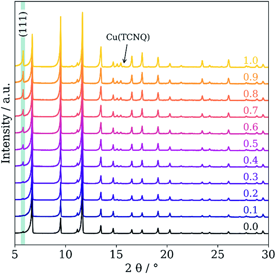 | ||
| Fig. 1 PXRD patterns of pristine Cu3BTC2 (black) and the concentration series of TCNQ-loaded Cu3BTC2. TCNQ loadings are given above each pattern as x in xTCNQ@Cu3BTC2. Traces of Cu(TCNQ) phase I can be found at high TCNQ loadings. | ||
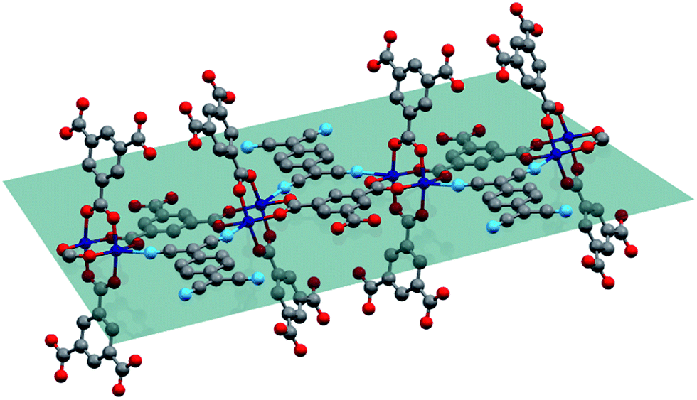 | ||
| Fig. 2 Schematic representation of TCNQ binding to the apical position of two neighbouring Cu paddlewheels directing the planar molecule into the (111) lattice plane (tile). For better visualization, the cubic symmetry is not applied. Cu, C, O, and N atoms are depicted in blue, grey, red, and light blue, respectively. | ||
In order to probe the porosity as function of x in xTCNQ@Cu3BTC2, we performed nitrogen adsorption experiments. As expected, a decrease of the Brunauer–Emmett–Teller (BET) surface area is observed, from 1833.0 m2 g−1 for pristine Cu3BTC2 to 573.7 m2 g−1 for 1.0TCNQ@Cu3BTC2 (Fig. 3), about two thirds of the initial BET surface area. In addition, the decrease is linear with TCNQ loading, providing additional evidence for the incorporation of the guest molecule into the framework. Importantly, the decrease cannot be explained by pore blocking or a simple adsorption of TCNQ at the crystal surface. For instance, the BET surface area of a physical mixture of both components for 1.0TCNQ@Cu3BTC2 would still amount to 1370.4 m2 g−1 (see detailed discussion in ESI†). It is further important to note that our measured surface areas considerably exceed those for TCNQ-loaded Cu3BTC2 samples reported in the literature. For example, the VPI 0.5TCNQ@Cu3BTC2 sample exhibits a surface area of 1145 m2 g−1, whereas the surface area of the material with the same loading synthesized via liquid phase infiltration is reported as 214 m2 g−1, which is likely due to residual adsorbed water or solvent.8
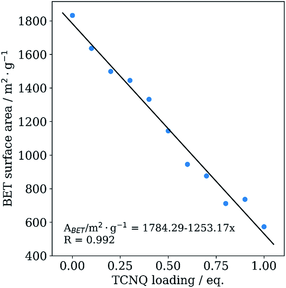 | ||
| Fig. 3 BET surface area of Cu3BTC2 samples plotted against the TCNQ loading amount. Values of the linear fit are shown in the diagram. | ||
The microstructure and phase homogeneity of the TCNQ-loaded samples was further investigated using SEM (Fig. 4). Nanowire-like structures were discovered on the external surface of the TCNQ-loaded MOF crystallites; the amount and dimensions of these increase with the amount of TCNQ employed during the VPI. To determine the chemical nature of the nanowires, scanning Auger electron microscopy was performed. These data show a homogenous distribution of Cu, C, and N (Fig. S13†). In combination with the characteristic morphology18 and the reflection at 15.77° in the diffraction pattern, the nanowires were identified as phase I of Cu(TCNQ). For the formation of Cu(TCNQ) to occur, both TCNQ and Cu(II) must be reduced to TCNQ− and Cu(I), presumably involving an oxidation (decarboxylation) of the BTC linker under the conditions of the loading experiment. In the elemental analysis data of the concentration series (Table S2†), slightly decreased carbon contents compared to the calculated values are found, whereas the nitrogen contents are slightly increased, supporting a decomposition of some BTC molecules. Moreover, Cu3BTC2 is known to contain small quantities of Cu(I) species, which have been related to intrinsic defects and thermal treatment during activation.19,20 Surface sensitive XPS measurements (Fig. S19†) reveal a relatively high abundance of Cu(I) species at the surface of Cu3BTC2 crystallites. This Cu(I) concentration is further increased by the inevitable prolonged thermal treatment during the VPI process. The Cu(I) species, in turn, are able to reduce neutral TCNQ (via Cu(I) → Cu(II) + e−) and thus enable the formation of the surface impurity phase Cu(TCNQ). The presence of several TCNQ species (i.e. coordinated, uncoordinated, radical anion) is suggested by the broadening of the N 1s signature in XPS (Fig. S20†). The formation of the Cu(TCNQ) byproduct could be reduced, but not fully inhibited, by using lower reaction temperatures (Fig. S15–S17†). However, reduced temperature also compromise the ordering of TCNQ, as evidenced by the absence of the pronounced (111) reflection in PXRD (Fig. S2†).
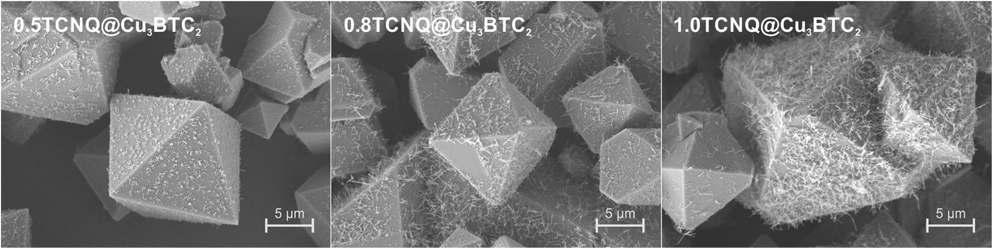 | ||
| Fig. 4 SEM images of Cu3BTC2 loaded with 0.5 (left), 0.8 (middle), and 1.0 (right) equivalents of TCNQ. Cu(TCNQ) nanowires form on the surface of the octahedral Cu3BTC2 crystallites and their amount and dimensions increase with higher loading. | ||
The loading and coordination of TCNQ to open Cu sites can also be tracked by vibrational spectroscopy. The infrared (IR) spectra of pristine and TCNQ-loaded Cu3BTC2 are shown in Fig. 5. Whereas in pristine Cu3BTC2 a band in the CN vibration region is absent, a CN vibration mode at 2222 cm−1 appears in TCNQ-loaded samples and becomes more pronounced with higher TCNQ loading. Notably, a second vibrational mode at 2200 cm−1 and a shoulder at 2170 cm−1 appear for samples with high TCNQ loading (cf. Fig. S6†). A red shift of the CN vibration was previously attributed to coordinated TCNQ involving a partial charge transfer.8,21 Due to the presence of the CuTCNQ byproduct in the samples, we here also assign some contribution to the signal at 2000 cm−1 and the shoulder at 2170 cm−1 to Cu(TCNQ), whose IR signature is known from the literature.22 The indication of multiple TCNQ species in the IR spectra matches well with the XPS signature in the N 1s regime.
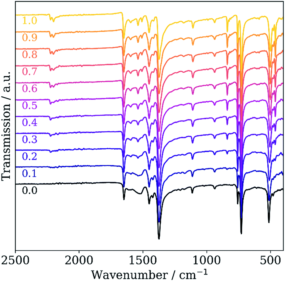 | ||
| Fig. 5 IR spectra of pristine Cu3BTC2 (black) and the concentration series of TCNQ-loaded Cu3BTC2. TCNQ loadings are given below each spectrum as x in xTCNQ@Cu3BTC2. | ||
Thermogravimetric analysis (TGA) of 1.0TCNQ@Cu3BTC2 (Fig. S7†) shows a decomposition that proceeds in one step with an onset at 300 °C. This temperature is slightly lower than observed for pristine Cu3BTC2, which starts to decompose at 330 °C. The corresponding features in the differential scanning calorimetry (DSC) data are at 349.7 °C and 338.3 °C for the pristine and the loaded MOF, respectively. The 1.0TCNQ@Cu3BTC2 sample shows an additional smaller peak at 314.2 °C, indicating a step-wise decomposition.
Electrical transport measurements were performed on pressed pellets using an air-tight two-point-probe setup. I–V curves were recorded from −5 V to 5 V (Fig. S9†) and the conductivity σ was calculated using eqn (1):
 | (1) |
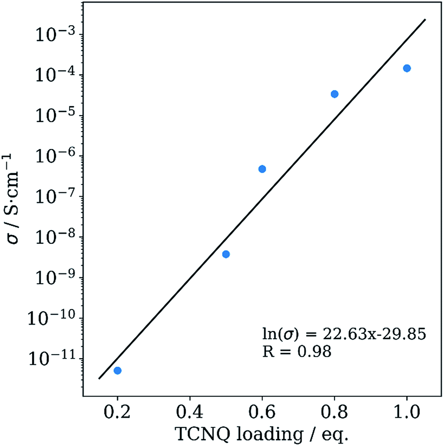 | ||
| Fig. 6 Electrical conductivity of TCNQ@Cu3BTC2 samples plotted against their TCNQ loading amount. | ||
The impact of the Cu(TCNQ) byproduct on the electrical transport, however, is intrinsically difficult to assess because Cu(TCNQ) can crystallize in two different phases. Phase II is a poor conductor, whereas phase I is an electrical semiconductor with a room temperature conductivity of 0.25 S cm−1.18 Mechanical removal of the nanowires by sonication was unsuccessful and led to a disordering of the TCNQ molecules and a significant decrease in the conductivity (Fig. S3, S11 and S18†). A physical mixture of 1% CuTCNQ/Cu3BTC2 (estimated amount from SEM images) did not show any conductivity. In combination with previous findings in the literature for TCNQ@HKUST-1 in which Cu(TCNQ) as an impurity phase was not observed, we ascribe the increasing electrical conductivity as function of TCNQ loading to the formation of our host–guest system. Moreover, 1.0TCNQ@Cu3BTC2 exhibits one of the highest-reported electrical conductivities paired with permanent porosity reported to date, comparing with other conductive MOFs of similar porosities, such as Cd2(TTFTB).6,26 The synthesis of a reference sample of xTCNQ@Cu3BTC2 (x = 0.4 as determined by EA) via liquid phase infiltration revealed no indication of TCNQ ordering, but a conductivity in the order of 10−1 S cm−1, which is significantly higher than for samples with comparable TCNQ loading prepared via VPI. However, this sample shows a non-ohmic behavior (deviation from the linear I–V curve) at high potentials that we assign to electrochemical processes of water/solvent inside the pores (Fig. S21–S24†). This finding emphasizes the importance of solvent exclusion during the guest infiltration step and highlights the need for in-depth structural and spectroscopic studies of Guest@MOF systems to develop and validate structure–property relationships.
Conclusions
We developed an optimized VPI strategy under thermodynamic control and used it to introduce stoichiometric amounts of TCNQ to obtain a concentration series of xTCNQ@Cu3BTC2 with 0 ≤ x ≤ 1.0 under strict inert conditions. No washing step is needed to remove excessive TCNQ, which is advantageous over the kinetically controlled loading procedure presented in previous studies.8–10,16 High reaction temperatures and long exposure times evidently promote an ordered, periodic arrangement of TCNQ within the (111) crystal lattice plane and the bridging coordination motif of TCNQ and the Cu atoms of two neighbouring paddle-wheel units. To our knowledge this is the first crystallographic evidence for the integration of TCNQ into the framework of Cu3BTC2, and further demonstrates that the introduction of a non-innocent guest molecule can be regarded as a new element of MOF property design. Additional evidence supporting the accommodation of TCNQ within the pores of the framework is the systematic decrease in the BET surface area. SEM images of the infiltrated samples show the formation of nanowires on the MOF crystal surface during VPI that were identified as Cu(TCNQ). Their formation can be reduced but not entirely suppressed at lower temperatures. IR data recorded during this work shows two nitrile vibration modes that can be attributed to TCNQ molecules inside the Cu3BTC2 framework and to the TCNQ anion in Cu(TCNQ). The electrical conductivity of the concentration series increases exponentially with the amount of TCNQ used in the VPI. Even though, a quantitative analysis of the contribution of the host–guest complex and the Cu(TCNQ) byproduct to the electrical conductivity of the material is difficult, the obtained material shows high conductivity values accompanied by high permanent porosity. In fact, the BET surface area of 1.0TCNQ@Cu3BTC2 is among the highest for electrically conductive MOFs.6,26 The combination of these two properties creates a high potential for using this material in sensing or electronic device fabrication where access to the pores provides an essential new function. In this respect, well defined, oriented Cu3BTC2 thin films deposited and infiltrated with TCNQ using solvent-free vapor phase techniques represent the ultimate goal. Pointing to the complexity of this system, further detailed analysis is required, beyond standard characterization techniques, to fully understand the ordering of TCNQ and the conductivity mechanism.Experimental
General information
All chemicals were purchased from commercial suppliers (ABCR, Acros Organics, Alfa Aesar, Sigma Aldrich) and used without further purification unless otherwise stated. Solvents used for the synthesis and washing steps were reagent grade or higher.Vapor phase infiltration
Cu3BTC2 was synthesized following the literature procedure.27 The tile crystalline product was continuously washed with ethanol and dichloromethane in a Soxhlet apparatus for one week, respectively, to rigorously remove all reactants and high-boiling solvents. The washing solution was replaced by the respective fresh solvent once. Subsequently, the blue powder was desolvated under high vacuum (∼10−6 mbar) at 180 °C to yield pristine Cu3BTC2. TCNQ was recrystallized three times from acetonitrile under inert conditions to yield molecular, crystalline TCNQ in high purity.Inside an argon glovebox, 200 mg of Cu3BTC2 and distinct amounts of TCNQ were physically mixed and filled into borosilicate glass tubes to prepare a concentration series of xTCNQ@Cu3BTC2 (x = n(TCNQ)/n(Cu3BTC2) with x = 0.1, 0.2,…, 1.0). The glass tube was then evacuated (∼10−3 mbar) and flame sealed to give a closed system for the VPI process. The sealed ampules were placed inside a convection oven at 180 °C for 72 hours allowing the TCNQ to sublime and diffuse into the MOF. After cooling down to room temperature the ampules were transferred into the glovebox and stored for further characterization.
Powder X-ray diffraction
Powder X-ray diffraction (PXRD) data was collected in a 2θ range of 5–50° in steps of 0.0016413° (2θ) on a PANalytical Empyrean equipped with a Cu X-ray tube operated at 45 kV and 40 mA. The samples were filled into borosilicate capillaries of 0.7 mm diameter and mounted onto a capillary spinner. The radiation was focused onto the sample through a focusing X-ray beam mirror equipped with a 1/8° divergence slit and 0.02 radian soller slits. The diffracted beam was detected by a PIXcel1D detector in receiving slit mode equipped with a 1/8° anti-scatter slit and 0.02 radian soller slits.Thermogravimetric analysis/differential scanning calorimetry
TGA/DSC measurements were carried out on a Mettler Toledo TGA/DSC 1 equipped with an auto sampler unit. Aluminum crucibles (100 μL) were filled with 5–10 mg of MOF powder inside the glovebox and tightly capped with an aluminum lit. The crucible was transferred into the TGA chamber and a hole was pinched into the lit while the stream of Ar (40 mL min−1) was already on. The temperature was ramped from 30 °C to 550 °C at a rate of 5 °C min−1. The instrument was calibrated to a blank sample prior to the measurements.Porosimetry measurements
Porosimetry measurements of pristine and guest-loaded MOF powders were performed using a Micromeritics 3flex to determine their BET surface area. Therefore, approximately 60 mg of a sample was filled into a BET tube and evacuated for 3 h at room temperature prior to the measurement. Nitrogen isotherms were recorded at 77 K. The BET surface area was calculated from data points in the relative pressure range of 0.01 to 0.1.Fourier transform infrared spectroscopy
Fourier transform infrared spectroscopy (FTIR) of powder samples was done in argon atmosphere on an ALPHA FTIR spectrometer (Bruker) equipped with a Pt attenuated total reflectance (ATR) unit at room temperature in the range of 400–4000 cm−1 with a resolution of 2 cm−1. 64 scans were recorded per measurement.Elemental analysis
Elemental analysis (EA) for the elements C, H, N, and S was carried out on a Hekatech EuroEA Elementaranalysator. Cu contents were determined by atom absorption spectroscopy (AAS) after decomposing the sample in a mixture of sulfuric acid and nitric acid in a CEM microwave.Scanning electron microscopy
Top-view micrographs of MOF powders were conducted on a Merlin high-resolution scanning electron microscope (Carl Zeiss) using an acceleration voltage of 5 kV. The samples were transferred from a glove box into the analysis chamber under argon atmosphere using a transfer vessel (Leica EM VC500). To avoid charging, the sample was coated with 5 nm of Pt prior to the measurement using a Leica EM ACE600. Energy dispersive X-ray spectroscopy (EDX) analysis was conducted using an XMAX EXTREME EDX detector (Oxford Instruments). Measurements were carried out by application of an acceleration voltage of 5 kV and a probing current of 100 pA for SEM and 1000 pA for EDX.Auger electron spectroscopy
AES measurements were performed at room temperature with a scanning Auger electron spectroscope (JEOL Ltd. JAMP-9500F field emission scanning Auger microprobe) system. Samples were prepared by spreading powder particles over a gold-coated surface. AES spectra were acquired with a primary beam of 10 keV. The take-off angle of the instrument was 0°. The differential energy spectrum was used to subtract background from the direct Auger spectrum for calculating the band-to-band intensity. The first differential d(N(E))/d(E) Auger spectra were obtained by numerical derivation of the direct N(E) integrated Auger data displaying an absolute scale with counts/second units by a universal Savitzky–Golay (SG) quadratic differential filter using seven points and used to calculate the band-to-band intensity of Auger electrons and derive the elemental compositions. The differential spectrum is simply the differential of the direct spectrum with respect to energy. The spectra were calibrated with the carbon band at 263.0 eV. For Auger elemental analysis an 8 nm probe diameter was used. Elemental mapping was analysed by AES. Elemental images were acquired with a primary beam of 10 keV. The take-off angle of the instrument was 0°. The coloured images are elemental distribution maps over the area shown in the upper right image (magnification 80![[thin space (1/6-em)]](https://www.rsc.org/images/entities/char_2009.gif) 000×).
000×).
X-ray photoelectron spectroscopy
XPS was carried out using a PHI5000 Versa Probe II (Physical Electronics GmbH) with an Al anode. To avoid air exposure, powder samples were transferred from an argon-filled glovebox to the analysis chamber using a transfer vessel filled with argon gas. The probed surface area was 100 μm × 1400 μm (i.e., X-ray spot size) and an X-ray power of 100 W was used. The pass energy of the analyzer was set to 23.5 eV for detail spectra and to 187.9 eV for survey scans. The chamber pressure was in the range of 10−7 Pa during the measurements. All spectra were charge corrected to a binding energy of 284.8 eV for the C 1s line corresponding to adventitious aliphatic carbon. Measurements were evaluated using CasaXPS V2.3.17 software.Electrical conductivity measurements
Inside an Ar filled glovebox, MOF powders (∼70 mg) were filled into an air-tight press cell and compressed uniaxially at 3 t (375 MPa) for 2 minutes. The press cell was mounted into an aluminium frame and fixed with a screw applying a torque of 10 Nm (cf. ESI Fig. 8†).28I–V curves were recorded between the two stainless steel electrodes of the press cell using an EC-Lab Electrochemistry SP-300 potentiostat/galvanostat (Bio-Logic Science Instruments). Conductivity measurements were carried out at 298 K (climate chamber, Weiss Klimatechnik, 1 h equilibration time) sweeping the voltage between 5 V and −5 V at a scan rate of 100 mV s−1.Conflicts of interest
There are no conflicts to declare.Acknowledgements
We thank Dr Vitalie Stavila and Dr Andrew Ullman for helpful discussions and Pia Vervoorts for help with BET measurements. Funding for this project was provided by the Sandia Laboratory Directed Research and Development (LDRD) Program. Sandia National Laboratories is a multimission laboratory managed and operated by National Technology and Engineering Solutions of Sandia, LLC, a wholly owned subsidiary of Honeywell International, Inc., for the U.S. Department of Energy’s National Nuclear Security Administration under contract DE-NA-0003525. CS acknowledges his scholarships from the German Academic Scholarship Foundation and from the German Chemical Industry Fund (FCI). RK acknowledges his scholarship from the FCI. This project was further supported by a PPP travel grant from the German Academic Exchange Service (DAAD).Notes and references
- I. Stassen, N. Burtch, A. Talin, P. Falcaro, M. Allendorf and R. Ameloot, Chem. Soc. Rev., 2017, 46, 3185–3241 RSC
.
- V. Stavila, A. A. Talin and M. D. Allendorf, Chem. Soc. Rev., 2014, 43, 5994–6010 RSC
- G. Maurin, C. Serre, A. Cooper and G. Ferey, Chem. Soc. Rev., 2017, 46, 3104–3107 RSC
- O. M. Yaghi, M. O'Keeffe, N. W. Ockwig, H. K. Chae, M. Eddaoudi and J. Kim, Nature, 2003, 423, 705–714 CrossRef PubMed
- M. Eddaoudi, J. Kim, N. Rosi, D. Vodak, J. Wachter, M. O'Keeffe and O. M. Yaghi, Science, 2002, 295, 469–472 CrossRef PubMed
- L. Sun, M. G. Campbell and M. Dincă, Angew. Chem., Int. Ed., 2016, 55, 3566–3579 CrossRef PubMed
- L. Sun, C. H. Hendon, S. S. Park, Y. Tulchinsky, R. Wan, F. Wang, A. Walsh and M. Dinca, Chem. Sci., 2017, 8, 4450–4457 RSC
- A. A. Talin, A. Centrone, A. C. Ford, M. E. Foster, V. Stavila, P. Haney, R. A. Kinney, V. Szalai, F. El Gabaly, H. P. Yoon, F. Léonard and M. D. Allendorf, Science, 2014, 343, 66–69 CrossRef PubMed
- X. Chen, Z. Wang, Z. M. Hassan, P. Lin, K. Zhang, H. Baumgart and E. Redel, ECS J. Solid State Sci. Technol., 2017, 6, 150–153 CrossRef
- T. Neumann, J. Liu, T. Wächter, P. Friederich, F. Symalla, A. Welle, V. Mugnaini, V. Meded, M. Zharnikov, C. Wöll and W. Wenzel, ACS Nano, 2016, 10, 7085–7093 CrossRef PubMed
- C. H. Hendon and A. Walsh, Chem. Sci., 2015, 6, 3674–3683 RSC
- K. J. Erickson, F. Léonard, V. Stavila, M. E. Foster, C. D. Spataru, R. E. Jones, B. M. Foley, P. E. Hopkins, M. D. Allendorf and A. A. Talin, Adv. Mater., 2015, 27, 3453–3459 CrossRef PubMed
- M. D. Allendorf, M. E. Foster, F. Léonard, V. Stavila, P. L. Feng, F. P. Doty, K. Leong, E. Y. Ma, S. R. Johnston and A. A. Talin, J. Phys. Chem. Lett., 2015, 6, 1182–1195 CrossRef PubMed
- W. Kaim and M. Moscherosch, Coord. Chem. Rev., 1994, 129, 157–193 CrossRef
- M. E. Peover, J. Chem. Soc., Faraday Trans., 1964, 60, 479–483 RSC
- P. M. Usov, H. Jiang, H. Chevreau, V. K. Peterson, C. F. Leong and D. M. D'Alessandro, J. Phys. Chem. C, 2017, 121, 26330–26339 CrossRef
- K. Schlichte, T. Kratzke and S. Kaskel, Microporous Mesoporous Mater., 2004, 73, 81–88 CrossRef
- R. A. Heintz, H. Zhao, X. Ouyang, G. Grandinetti, J. Cowen and K. R. Dunbar, Inorg. Chem., 1999, 38, 144–156 CrossRef
- N. Nijem, H. Bluhm, M. L. Ng, M. Kunz, S. R. Leone and M. K. Gilles, Chem. Commun., 2014, 50, 10144–10147 RSC
- J. Szanyi, M. Daturi, G. Clet, D. R. Baer and C. H. F. Peden, Phys. Chem. Chem. Phys., 2012, 14, 4383–4390 RSC
- J. S. Chappell, A. N. Bloch, W. A. Bryden, M. Maxfield, T. O. Poehler and D. O. Cowan, J. Am. Chem. Soc., 1981, 103, 2442–2443 CrossRef
- M. Inoue and M. B. Inoue, J. Chem. Soc., Faraday Trans. 2, 1985, 81, 539–547 RSC
- L. Sun, S. S. Park, D. Sheberla and M. Dincă, J. Am. Chem. Soc., 2016, 138, 14772–14782 CrossRef PubMed
- B. Abeles, H. L. Pinch and J. I. Gittleman, Phys. Rev. Lett., 1975, 35, 247–250 CrossRef
- B. J. Last and D. J. Thouless, Phys. Rev. Lett., 1971, 27, 1719–1721 CrossRef
- M. L. Aubrey, B. M. Wiers, S. C. Andrews, T. Sakurai, S. E. Reyes-Lillo, S. M. Hamed, C.-J. Yu, L. E. Darago, J. A. Mason, J.-O. Baeg, F. Grandjean, G. J. Long, S. Seki, J. B. Neaton, P. Yang and J. R. Long, Nat. Mater., 2018, 17, 625–632 CrossRef PubMed
- M. K. Bhunia, J. T. Hughes, J. C. Fettinger and A. Navrotsky, Langmuir, 2013, 29, 8140–8145 CrossRef PubMed
- W. Zhang, D. A. Weber, H. Weigand, T. Arlt, I. Manke, D. Schröder, R. Koerver, T. Leichtweiss, P. Hartmann, W. G. Zeier and J. Janek, ACS Appl. Mater. Interfaces, 2017, 9, 17835–17845 CrossRef PubMed
Footnote |
| † Electronic supplementary information (ESI) available: Experimental details, PXRD patterns, BET surface area analysis, IR spectra, thermogravimetric analysis, current–voltage curves, Auger electron spectroscopy, SEM images, XPS spectra, elemental analysis. See DOI: 10.1039/c8sc02471e |
| This journal is © The Royal Society of Chemistry 2018 |