
Brilliant triboluminescence in a potential organic–inorganic hybrid ferroelectric: (Ph3PO)2MnBr2†
Yuan-Yuan
Tang
a,
Zhong-Xia
Wang
a,
Peng-Fei
Li
a,
Yu-Meng
You
*a,
Alessandro
Stroppa
bc and
Ren-Gen
Xiong
a
aOrdered Matter Science Research Center, Southeast University, Nanjing, 211189, P. R. China. E-mail: youyumeng@seu.edu.cn; Tel: +86-25-52090626
bConsiglio Nazionale delle Ricerche (CNR-SPIN), Via Vetoio, I-67010 L'Aquila, Italy
cInternational Centre for Quantum and Molecular Structures, and Physics Department, Shanghai University, Shanghai, 200444, P. R. China
First published on 18th November 2016
Abstract
Ferroelectrics with luminescent properties are promising candidates for the next generation of optical waveguides and displays. However, reports on ferroelectrics with triboluminescence properties have been very scarce so far. In this study, we demonstrate a potential hybrid molecular ferroelectric, (Ph3PO)2MnBr2, which exhibits intense green triboluminescence. Using piezoresponse force microscopy, the presence of ferroelectric domains in (Ph3PO)2MnBr2 thin films is confirmed. We also show evidence for the reversible switching of the ferroelectric domains by poling with DC biases. We believe that this combination of ferroelectricity and triboluminescence will bring about potential multifunctional optoelectronic device applications.
Introduction
The emission of light caused by mechanical excitation (motion or stress) in solid materials is designated triboluminescence (TrL, also called mechanoluminescence).1,2 TrL has in fact been known for at least 400 years, with one of the earliest references, to sugar, showing up in Francis Bacon's “The Advancement of Learning” in 1605.3 Since the beginning of the 21st century, triboluminescent materials have been investigated for applications in bioimaging,4 as a source of X-rays5 and as real-time structural damage sensors,6 which can be exploited in both commercial and military markets. The luminescence properties of ferroelectrics, such as their electroluminescence,7 cathodoluminescence8 and photoluminescence,9–12 have attracted great interest for their potential applications in the next generation of optical waveguides and displays. For instance, Al3+-doped SrTiO3:Pr3+ exhibits red cathodoluminescence, which can be excited at a low anode voltage and reaches an efficiency as high as 0.4 lm W−1, affording it promising applications in field emission displays (FEDs), vacuum fluorescent displays, etc.8,13 However there are rarely reports of triboluminescence properties in ferroelectrics.During the last decade, organic–inorganic hybrid compounds have attracted intensive attention in the field of optoelectronic materials, with the concomitant fabrication of materials with great tenability offering unique physical properties.14–26 The potential of triboluminescent ferroelectric materials relies on utilizing the synergy between the intrinsic characteristics of the organic components (which are flexible, lightweight, large-area, and low-cost) and the luminescence features of the metal ions (i.e. a high luminescence quantum yield, long lifetime, and narrow emission bandwidth).9,26 It is expected that the introduction of ferroelectricity into triboluminescent organic–inorganic hybrids will lead to potential multifunctional optoelectronic device applications.
Since 1961, several organic–inorganic hybrid manganese(II) complexes including (Ph3PO)2MnX2 (X = Cl, Br, I), which crystallize in non-centrosymmetric space groups, have been found to exhibit brilliant TrL.27 Among those materials, the room-temperature crystal structure of (Ph3PO)2MnBr2 (1) adopts a polar space group (P1), fulfilling the symmetry requirement for ferroelectricity. In this context, therefore, we study its potential ferroelectric properties. The appearance of switchable electric polarization indicating ferroelectricity was confirmed using piezoresponse force microscopy (PFM)28–31—an ideal tool for probing the local ferroelectric response on the microscopic scale. PFM is based on atomic force microscopy (AFM), in which an AC voltage is applied to a scanning conductive tip in contact with the sample surface. Since all ferroelectric materials are also piezoelectric, when the tip is in contact with the surface, the local piezoelectric response would be detected as the first harmonic component of the tip deflection, and then the phase and amplitude of the electromechanical response of the surface yield information on the ferroelectric domain orientations and domain wall positions below the tip, respectively. Finally, the electromechanical response can be probed as a function of the DC bias of the tip, providing information on the switching of the domains.28,32 If the applied field is large enough (e.g. greater than the local coercive field), it can cause ferroelectric polarization reversal. In this manner, we have directly imaged domains and domain walls in (Ph3PO)2MnBr2 thin films using PFM, and successfully switched the ferroelectric domains reversibly through the application of a DC bias.
Experimental section
Synthetic procedures
Ph3PO (triphenylphosphine oxide) (10 mmol, 2.78 g) and MnBr2·4H2O (5 mmol, 1.44 g) were dissolved in ethanol (10 mL), separately. Then, the two solutions were mixed and continuously stirred for 30 min at room temperature. The reaction mixture was filtered and left to stand for several days. Green block crystals of 1 suitable for X-ray analyses were obtained. In the IR spectra of 1 (Fig. S1, ESI†), the peak at approximately 3058 cm−1 is assigned to the stretching vibration absorption of![[double bond, length as m-dash]](https://www.rsc.org/images/entities/char_e001.gif) C–H in the phenyl group, which reveals the existence of Ph3PO in 1. The phase purity of 1 is verified by the powder XRD (PXRD) pattern, which matches very well with the pattern simulated from the single-crystal structure at room temperature (Fig. S2†). 1 is insoluble in water, and its solubility in methanol is about 0.6 g ml−1. Elemental analysis, calcd (%) for 1: C, 56.06; H, 3.92. Found: C, 56.20; H, 4.08. The paramagnetism of 1 was also confirmed by magnetic measurements (Fig. S7†).
C–H in the phenyl group, which reveals the existence of Ph3PO in 1. The phase purity of 1 is verified by the powder XRD (PXRD) pattern, which matches very well with the pattern simulated from the single-crystal structure at room temperature (Fig. S2†). 1 is insoluble in water, and its solubility in methanol is about 0.6 g ml−1. Elemental analysis, calcd (%) for 1: C, 56.06; H, 3.92. Found: C, 56.20; H, 4.08. The paramagnetism of 1 was also confirmed by magnetic measurements (Fig. S7†).
Thin film fabrication
Ferroelectric thin films of compound 1 were grown by a spin-coating method. To be specific, 128.3 mg of crystals of 1 were dissolved into 0.5 ml of methanol to form a clear precursor solution. Then 20 μl of the above solution was spin-coated on an ITO-coated glass substrate at 6000 rpm for 40 seconds, and finally the film was annealed at 75 °C for 5 min to remove the solvent and further improve the crystallinity.PFM measurement
Visualization of the ferroelectric domain structures was carried out on a commercial atomic force microscope system (MFP-3D, Asylum Research). Conductive Pt/Ir-coated silicon probes (EFM-50, Nanoworld) were used for the domain imaging and polarization switching studies. The resonant-enhanced PFM mode was applied to enhance the signal, with a typical AC voltage of 5.0 V at ∼360 kHz.UV-vis transmission spectrum
The UV-vis spectrum of 1 was obtained from a powder sample of 1 at room temperature on a Shimadzu UV-2600 spectrophotometer mounted with an ISR-2600 Plus integrating sphere.Photoluminescence and triboluminescence
The corresponding spectra were measured on a Shimadzu RF-5301pc fluorescence spectrophotometer at room temperature.Results and discussion
The X-ray structure determination reveals that 1 displays a mononuclear structure and crystallizes in the polar space group P1 at room temperature, with cell parameters of a = 10.013(7) Å, b = 10.253(7) Å, c = 10.564(6) Å, α = 65.31(6)°, β = 63.75(5)°, γ = 89.72(7)°, V = 862.0 Å3 and Z = 1 (Table S1†). The asymmetric unit of 1 contains one Mn(II) center, two Ph3PO organic ligands and two Br− ions (Fig. 1). The Mn(II) atom is four-coordinated by two oxygen atoms from two chelating Ph3PO ligands and by two Br− anions. The coordination geometry around the Mn(II) atom can be described as a distorted tetrahedron, where the angles vary from 102.6 (3) to 114.94 (9)° and the average Mn–O bond distance (2.044(7) Å) and Mn–Br bond distance (2.4695(3) Å) are distinct.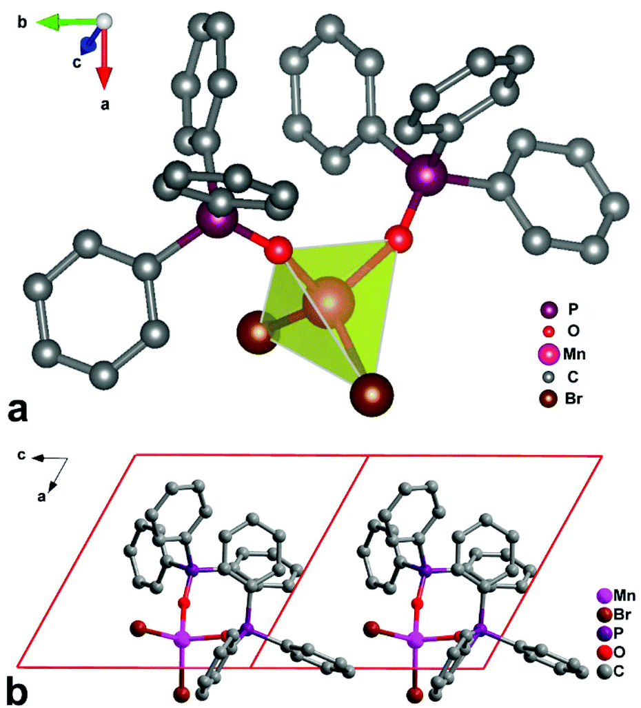 | ||
| Fig. 1 (a) Asymmetric unit of 1 at room temperature. (b) Packing diagrams viewed along the b axis at room temperature. | ||
A thin film of compound 1 can be simply fabricated by low temperature solution processing due to its organic–inorganic hybrid nature. PFM testing was carried out on the thin film sample of 1 to characterize its ferroelectric properties. Fig. 2a shows a 5 × 5 μm2 AFM image (contact mode) revealing a grain size on the order of 0.1–1 μm. Fig. 2b and c present the images constructed from the out-of-plane PFM amplitude and phase, respectively, which distinctly reveal the static domain structure for the thin film of compound 1. The PFM amplitude directly measures the piezoelectric coefficient of a crystal surface, whereas the phase of the piezoresponse signal represents the direction of the polarization. Antiparallel domains can be seen in the phase image (Fig. 2c), with the yellow and purple contrast indicating the different polarization orientations of the domains. The dark hatched regions between the different domains in the corresponding amplitude image (Fig. 2b) are due to the domain walls, indicated by regions where the phase shifts 180°. Note that distinct differences of amplitude contrast emerge between the two antiparallel domains and even in the parallel domains. This is mainly because the polycrystalline film is composed of grains with various crystallographic orientations, which possess different polarization orientations.
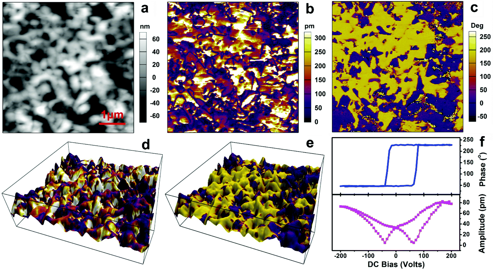 | ||
| Fig. 2 Topographic image (a), and vertical PFM amplitude (b) and phase images (c) for the thin film of compound 1. Amplitude mapping (d) and phase mapping (e) of the vertical PFM overlaid on the 3D topography. (f) Phase and amplitude signals as functions of the tip voltage for a selected point, showing the local PFM hysteresis loops. | ||
To eliminate the interference from topographic artifacts and thereby verify the domain structure,33 the piezoresponse has been overlaid on a three-dimensional (3D) topograph (Fig. 2d and e), in which the color contrast shows the amplitude and phase of the piezoresponse with the same color scales as depicted in Fig. 2b and c, respectively. It is clear that the piezoresponse (especially the phase) has no obvious correlation with the local topology of the sample surface. The domain structures display irregular shapes, while the domains are of various size scales. Some of the grains contain two antiparallel domains variously oriented among the crystallographically allowable directions of that grain. In addition, the domain walls are not completely coincident with the grain boundaries. Therefore, Fig. 2 presents direct experimental proof for the existence of ferroelectric domains in the thin film of compound 1.
In general, PFM measurements can simultaneously obtain information on the out-of-plane component of the electromechanical surface response—i.e., normal to the film plane (vertical PFM, or VPFM), as well as on the in-plane component through the frictional forces (lateral PFM, or LPFM).34,35 Fig. S3† depicts typical vertical and lateral PFM mappings in another region over an area of 5 × 5 μm2. The phase and amplitude images acquired with vertical PFM correspond well to each other, revealing a similar ferroelectric domain pattern to that in Fig. 2; no crosstalk with the topography is observed. Lateral PFM shows phase and amplitude images different from the vertical one, indicating the diverse polarization distributions in these two PFM modes. The real space reconstruction of the polarization orientation is derived from three components of the piezoresponse: vertical PFM plus at least two orthogonal lateral PFM measurements. Hence, the various orientations of the crystal grains can give rise to the differences in the PFM amplitude and phase signals of the thin film between the out-of-plane and in-plane components. Accordingly, the presence of ferroelectric domains in the thin film of compound 1 is further verified by Fig. S3.†
In ferroelectric materials, the most crucial property is the switchable spontaneous polarization, which describes the phenomenon of switching between two spontaneously polarized states under electrical or mechanical loads.28,29,33,35 Local PFM spectroscopic measurement for the film is carried out (Fig. 2f), with an applied DC voltage to switch the polarization, exhibiting bipolar piezoelectric hysteresis loops. This result is solid proof of 180° polarization reversal occurring under the applied bias voltage, which is typical for the switching of the ferroelectric polarization. The local coercive voltages for a selected point are about +60.0 and −40.0 V, as indicated by the minima of the amplitude loop. To visualize the polarization switching, we carried out a point polarization study. By applying a large DC voltage between the conductive tip and the ITO substrate, one can reverse the direction of the polarization on the point of interest. Fig. 3 presents the results of an experiment aimed at poling the ferroelectric domains in the thin film of compound 1. The left column in Fig. 3 presents height images (the topography) of a single 5 × 5 μm2 area, repeatedly scanned with AFM (in contact mode). The middle and right columns are simultaneously acquired vertical PFM amplitude and phase images, respectively, of the exact same area.
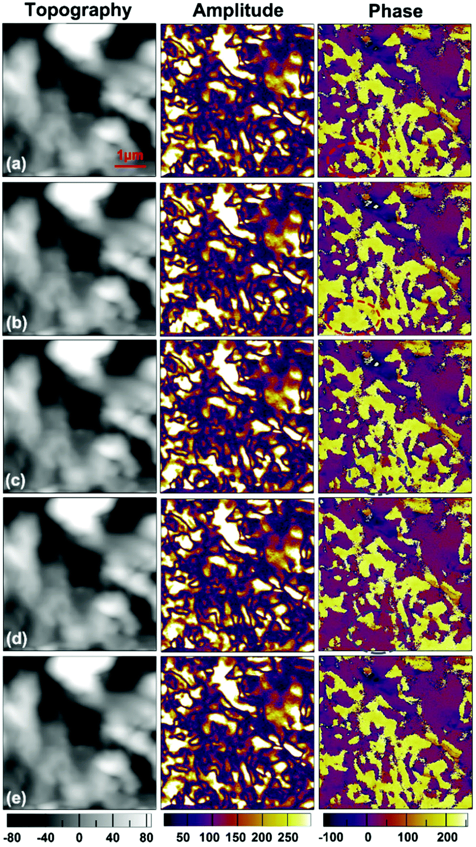 | ||
| Fig. 3 Topographic images (left), and PFM amplitude (middle) and phase (right) images of the crystal surface. (a) The initial state. (b) After the first switching with a negative bias at −120 V for 5 s. (c) The state after about 5 minutes. (d) After the second switching with a positive bias at +80 V for 5 s. (e) The state after about 5 minutes. The bias was applied at the centers of the dashed ellipses. The yellow and purple regions in the phase images indicate the regions with polarizations oriented upward and downward, respectively. | ||
Firstly, the PFM image of the as-grown film is obtained with an AC voltage of 5.0 V between the conductive tip and substrate (Fig. 3a). Then a region can be polarized with an electrically biased PFM tip: the center of the red dashed ellipse in the phase image of Fig. 3a is the point poled with a tip for 5 s under a −120 V bias exceeding the coercive voltage. As illustrated in Fig. 3b, the phase image shows that the purple region inside the ellipse mostly changes to yellow, revealing that the polarization state of this area has switched upwards, which coincides with the shift of the domain walls suggested by the amplitude image. Thus, the yellow and purple regions in the phase image represent the regions with polarizations oriented upward and downward, respectively, in their vertical component. Interestingly, the domain structure reverts to its initial state when it is examined about 5 minutes later (Fig. 3c). This spontaneous back-switching might result from the presence of an internal bias created by trapped charge carriers, making the original domain configuration advantageous over the switched one.28 A further study is desired to elucidate the minute mechanism of the domain relaxation.
After subsequent poling for the same period (5 s) with an opposite bias of +80 V on the tip, the polarization direction of another selected region can also be switched, as shown in the phase and amplitude images (Fig. 3d). This observation confirms that a different polarization can be printed as a domain within the opposite polarization region; that is, the domains in the film surface of 1 can be switched by an external field. The domain structure reverts to its initial state again about 5 minutes later (Fig. 3e). Moreover, when the same yellow region is point poled again for 5 s at +50 V, the sizes of the areas switched are smaller than those of the areas poled at +80 V (Fig. S4c†). It should be noted that the topographic image of the same area of the film, obtained after these procedures, does not show any traces of surface deformation. The piezoresponse, on the other hand, absolutely depends on the poling DC bias magnitude and polarity. The PFM results demonstrate switchable and stable polarization, the characteristic feature of a ferroelectric material, which distinguishes them from piezoelectric and pyroelectric materials.
In addition to ferroelectric properties, 1 shows intriguing luminescence properties. The optical absorption properties of 1 were investigated by obtaining a solid state UV-vis transmission spectrum at room temperature. As shown in Fig. S5,† it displays several intense absorption bands from 200 to 700 nm. Especially in the visible region, the absorption capacity for blue light is much stronger than that for green and red light, corresponding well with the yellowish-green appearance of the bulk crystal. Meanwhile, the as-grown crystals also show extraordinarily strong green light emission. By resonantly exciting the crystal at wavelengths from 330 to 355 nm, photoluminescence (PL) spectra at different excitation wavelengths were recorded and are listed in Fig. 4a. In the PL spectra, a strong emission can be observed at 512 nm, with a position that does not shift as a function of the excitation wavelength. This emission originates from the tetrahedrally coordinated manganese. While a nearly constant emission energy of 2.42 eV (512 nm) is observed, the PL intensity increases upon increasing the excitation wavelength in the range of 330 to 355 nm, which is more clearly demonstrated by the photoluminescence excitation (PLE) spectrum with an emission wavelength fixed at 512 nm. From the PLE curve recorded in Fig. 4a, the green emission at 512 nm is actually a mirror image of the PLE peak located at 471 nm, with a typical Stokes Shift of 41 nm. More interestingly, this emission can also be achieved by mechanical friction. Such a phenomenon was reported by F. A. Cotton et al. in 1961.27 As shown in Fig. 4b, a triboluminescence spectrum was obtained by repeatedly measuring the light emission of the crystal upon applying mechanical friction. The normalized TrL spectrum has the same trend as the PL spectrum, indicating the same radiative recombination path from the excited state back to the ground state.
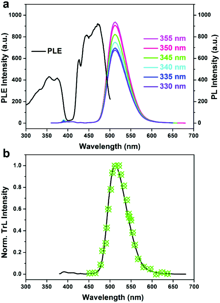 | ||
| Fig. 4 (a) Photoluminescence excitation (PLE) and photoluminescence (PL) spectra of 1. (b) Normalized triboluminescence spectrum of 1, where the black solid line indicates its PL spectrum. | ||
Conclusions
In summary, we have shown bright green triboluminescence in a potential hybrid ferroelectric compound: (Ph3PO)2MnBr2. The presence of ferroelectric domains in (Ph3PO)2MnBr2 thin films is confirmed using piezoresponse force microscopy. Furthermore, we also show evidence for the reversible switching of the ferroelectric domains by poling with a DC bias. Combining the triboluminescence properties, structural flexibility, and ferroelectricity, our studies provide a new approach to fabricating multifunctional optoelectronic devices, which could eventually benefit the application of optoelectronics and photovoltaics.Acknowledgements
A. S. thanks the High-End Foreign Expert program hosted by Shanghai University. This work was supported by the National Natural Science Foundations of China (Grant No. 21541013), and Natural Science Foundations of Jiangsu (Grant No. BK20150596 and BK20160029).Notes and references
- A. J. Walton, Adv. Phys., 2006, 26, 887–948 CrossRef.
- C. Hurt, N. McAvoy, S. Bjorklund and N. Filipescu, Nature, 1966, 212, 179–180 CrossRef CAS.
- F. Bacon, The Advancement of Learning, Macmillan, 1895 Search PubMed.
- N. Terasaki, H. Zhang, H. Yamada and C. N. Xu, Chem. Commun., 2011, 47, 8034–8036 RSC.
- C. G. Camara, J. V. Escobar, J. R. Hird and S. J. Putterman, Nature, 2008, 455, 1089–1092 CrossRef CAS.
- I. Sage and G. Bourhill, J. Mater. Chem., 2001, 11, 231–245 RSC.
- L. Godefroy, P. Jullien, B. Morlon and G. Godefroy, Ferroelectrics, 2011, 8, 421–423 CrossRef.
- H. Yamamoto, S. Okamoto and H. Kobayashi, J. Lumin., 2002, 100, 325–332 CrossRef CAS.
- Y. Zhang, W. Q. Liao, D. W. Fu, H. Y. Ye, Z. N. Chen and R. G. Xiong, J. Am. Chem. Soc., 2015, 137, 4928–4931 CrossRef CAS PubMed.
- Y. Liu, C.-N. Xu, K. Nonaka and H. Tateyama, Ferroelectrics, 2001, 264, 331–336 CrossRef CAS.
- R.-G. Xiong and X.-Z. You, Inorg. Chem. Commun., 2002, 5, 677–681 CrossRef CAS.
- C. Tao, J. Wu, Y. Yan, C. Shi and J. Li, Inorg. Chem. Front., 2016, 3, 541–546 RSC.
- P. S. Pizani, E. R. Leite, F. M. Pontes, E. C. Paris, J. H. Rangel, E. J. H. Lee, E. Longo, P. Delega and J. A. Varela, Appl. Phys. Lett., 2000, 77, 824–826 CrossRef CAS.
- T. Besara, P. Jain, N. S. Dalal, P. L. Kuhns, A. P. Reyes, H. W. Kroto and A. K. Cheetham, Proc. Natl. Acad. Sci. U. S. A., 2011, 108, 6828–6832 CrossRef.
- Y.-S. Meng, C.-H. Wang, Y.-Q. Zhang, X.-B. Leng, B.-W. Wang, Y.-F. Chen and S. Gao, Inorg. Chem. Front., 2016, 3, 828–835 RSC.
- Z. Sun, Y. Tang, S. Zhang, C. Ji, T. Chen and J. Luo, Adv. Mater., 2015, 27, 4795–4801 CrossRef CAS PubMed.
- S. Chen, R. Shang, K.-L. Hu, Z.-M. Wang and S. Gao, Inorg. Chem. Front., 2014, 1, 83–98 RSC.
- Y. Zhang, H.-Y. Ye, W. Zhang and R.-G. Xiong, Inorg. Chem. Front., 2014, 1, 118–123 RSC.
- G. C. Xu, W. Zhang, X. M. Ma, Y. H. Chen, L. Zhang, H. L. Cai, Z. M. Wang, R. G. Xiong and S. Gao, J. Am. Chem. Soc., 2011, 133, 14948–14951 CrossRef CAS PubMed.
- Z. Y. Du, T. T. Xu, B. Huang, Y. J. Su, W. Xue, C. T. He, W. X. Zhang and X. M. Chen, Angew. Chem., Int. Ed., 2015, 54, 914–918 CrossRef CAS PubMed.
- W.-B. Sun, B. Yan, Y.-Q. Zhang, B.-W. Wang, Z.-M. Wang, J.-H. Jia and S. Gao, Inorg. Chem. Front., 2014, 1, 503–509 RSC.
- L. Li, S. Zhang, L. Xu, J. Wang, L.-X. Shi, Z.-N. Chen, M. Hong and J. Luo, Chem. Sci., 2014, 5, 3808–3813 RSC.
- X. Liu, W. Zhao, H. Cui, Y. a. Xie, Y. Wang, T. Xu and F. Huang, Inorg. Chem. Front., 2015, 2, 315–335 RSC.
- T. Akutagawa, H. Koshinaka, D. Sato, S. Takeda, S. Noro, H. Takahashi, R. Kumai, Y. Tokura and T. Nakamura, Nat. Mater., 2009, 8, 342–347 CrossRef CAS PubMed.
- D.-X. Zhang, H.-X. Zhang, T. Wen, D.-S. Li and J. Zhang, Inorg. Chem. Front., 2016, 3, 263–267 RSC.
- Z. Sun, X. Liu, T. Khan, C. Ji, M. A. Asghar, S. Zhao, L. Li, M. Hong and J. Luo, Angew. Chem., Int. Ed., 2016, 55, 6545–6550 CrossRef CAS PubMed.
- D. M. Goodgame and F. Cotton, J. Chem. Soc., 1961, 3735–3741 RSC.
- A. Gruverman, O. Auciello and H. Tokumoto, Annu. Rev. Mater. Sci., 1998, 28, 101–123 CrossRef CAS.
- S. V. Kalinin, B. J. Rodriguez, S. Jesse, Y. H. Chu, T. Zhao, R. Ramesh, S. Choudhury, L. Q. Chen, E. A. Eliseev and A. N. Morozovska, Proc. Natl. Acad. Sci. U. S. A., 2007, 104, 20204–20209 CrossRef CAS PubMed.
- S. Horiuchi, Y. Noda, T. Hasegawa, F. Kagawa and S. Ishibashi, Chem. Mater., 2015, 27, 6193–6197 CrossRef CAS.
- X. Peng, Y. Rong, L. Fan, K. Lin, H. Zhu, J. Deng, J. Chen and X. Xing, Inorg. Chem. Front., 2015, 2, 1091–1094 RSC.
- B. D. Huey, R. Nath Premnath, S. Lee and N. A. Polomoff, J. Am. Ceram. Soc., 2012, 95, 1147–1162 CrossRef CAS.
- Y. Kutes, L. Ye, Y. Zhou, S. Pang, B. D. Huey and N. P. Padture, J. Phys. Chem. Lett., 2014, 5, 3335–3339 CrossRef CAS PubMed.
- L. M. Eng, H.-J. Güntherodt, G. A. Schneider, U. Köpke and J. Muñoz Saldaña, Appl. Phys. Lett., 1999, 74, 233–235 CrossRef CAS.
- S. V. Kalinin and A. Gruverman, Scanning probe microscopy: electrical and electromechanical phenomena at the nanoscale, Springer Science & Business Media, 2007 Search PubMed.
Footnote |
| † Electronic supplementary information (ESI) available: Crystallographic data, IR spectra, PXRD data, UV-vis absorption spectrum, and vertical and lateral PFM mappings for (Ph3PO)2MnBr2. CCDC 1478997. For ESI and crystallographic data in CIF or other electronic format see DOI: 10.1039/c6qi00148c |
| This journal is © the Partner Organisations 2017 |