 Open Access Article
Creative Commons Attribution 3.0 Unported Licence
High thermoelectric performance of rapidly microwave-synthesized Sn1−δS†‡
Jesús
Prado-Gonjal
 *ab,
Javier
Gainza
 b,
Isabel
Aguayo
a,
Óscar Juan
Durá
 c,
Sara
Rodríguez-Pérez
a,
Federico
Serrano-Sánchez
 b,
Norbert M.
Nemes
 d,
María Teresa
Fernández-Díaz
e,
José Antonio
Alonso
 b and
Emilio
Morán
a
aDepartamento de Química Inorgánica, Universidad Complutense de Madrid, E-28040 Madrid, Spain. E-mail: jpradogo@ucm.es
bInstituto de Ciencia de Materiales de Madrid (ICMM), Consejo Superior de Investigaciones Científicas (CSIC), Sor Juana Inés de la Cruz 3, E-28049, Madrid, Spain
cDepartamento de Física Aplicada, Universidad de Castilla-La Mancha, Ciudad Real, E-13071, Spain
dDepartamento de Física de Materiales, Universidad Complutense de Madrid, E-28040 Madrid, Spain
eInstitute Laue Langevin, BP 156X, Grenoble, F-38042, France
First published on 12th June 2020
Abstract
Phase-pure polycrystalline Sn1−δS has been prepared using a one-step microwave-hydrothermal procedure. Its structural characterization by neutron powder diffraction and transmission electron microscopy shows an orthorhombic Pnma phase at room temperature with the presence of a significant amount of Sn vacancies (Sn0.87S), randomly located in the crystal structure. This work proves that this inexpensive 2D material, constituted by high abundance elements, is a promising candidate for thermoelectric applications. This is confirmed by its relatively high carrier density and good mobility (2.5 × 1018 cm−3 and 13 cm2 V−1 s−1 at room temperature, respectively) found in the microwave-hydrothermal-synthesized sample, which favours high thermoelectric performance. In addition, a remarkably high Seebeck coefficient (682 μV K−1) combined with low electrical resistivity (5.6 × 10⁻⁴ Ω m) and thermal conductivity (0.57 W m−1 K−1) at 523 K produces a reasonably high figure of merit ZT of 0.76.
Introduction
The climate and environmental emergency have motivated increasing research on alternative sources of energy. For this reason, thermoelectric (TE) technology is an encouraging option due to the capability of producing electricity from waste heat.1 A TE device encloses several TE couples of n-type and p-type semiconductors electrically wired in series and thermally connected in parallel.2 When a temperature gradient is created, an electrical potential is generated due to the Seebeck effect.3–5The effectiveness of a TE device is directly related to the electrical and thermal properties of the semiconducting materials of which it is composed. The materials’ performance is typically determined by the dimensionless figure of merit (ZT) equation (eqn (1)).6,7 High thermoelectric performance includes the uncommon conjunction of a low electrical resistivity (ρ) and a high Seebeck coefficient (S) together with a low thermal conductivity (κ = κL + κe). The last includes the contributions of lattice thermal conductivity (κL) and electronic thermal conductivity (κe).8–10 All TE properties are strongly coupled to the crystal lattice, to the electronic structure and to the carrier concentration of the material as well.11
 | (1) |
There is an intense search for new materials with an improved thermoelectric efficiency. The representative examples are Bi2Te3,12,13 PbTe,14,15 SiGe,16,17 GeTe,18,19 Zintl phases,20,21 metal silicides,22,23 skutterudites,24–26 half-Heusler alloys27–29 and clathrates.30,31 It is essential to mention that, in 2014, an unprecedented ZT value of 2.6 at 923 K along the b-crystallographic axis was found for SnSe in the form of a single crystal.32 Above 750 K, SnSe undergoes a second order displacive phase transition from orthorhombic Pnma to a higher-symmetry orthorhombic Cmcm structure. This outstanding result is mainly attributed to the low lattice thermal conductivity found for the phase, which is intimately associated with the strong vibrational anharmonicity of the anisotropic 2D crystal structure.33–35
By means of first principles calculations, Aseginolaza et al.36 determined that the electronic properties of isostructural and isoelectronic SnS and SnSe are analogous, while Hao et al.37 found the ZT values of hole doped SnS-based crystals to range from 1.3 at 300 K (Pnma phase) to 1.9 at 800 K (Cmcm phase). Furthermore, recent studies have suggested that it is feasible to control the thermoelectric properties of polycrystalline SnS by tuning the charge carrier concentration (holes) with Sn vacancy engineering.38 This indicates that there is enormous potential to make significant advances in the preparation of environmentally friendly SnS-based compounds, which are constituted by low-cost and high abundance elements and can be considered as appealing TE materials for large-scale applications.38,39
Tin chalcogenides, and specifically SnS, are generally produced by a prolonged annealing process (days) of stoichiometric amounts of high-purity precursors in an evacuated sealed tube.40 This effective method presents some disadvantages, such as the need of operating at high temperatures to accelerate the diffusion between precursors, a non-accurate control of the stoichiometry when using volatile reagents (as sulphur) and the need for intermediate grindings, besides being a high energy and time consuming process. Accordingly, there is a strong motivation to find alternative synthesis pathways, where the energy requirements for the synthesis and the reaction time are considerably minimized. Among these methods, ball-milling, arc-melting and high-pressure synthesis have become attractive alternatives for the preparation of thermoelectric materials.41–46 In the present work, we would like to emphasize that microwave-assisted synthesis is also a powerful method to consider. This is a “Fast Chemistry” method that has not been extensively studied for the preparation of thermoelectric materials yet,47–49 but has emerged for the synthesis of a plethora of other non-molecular materials (especially oxides) with different structures, properties and applications.50–52 The decrease in the reaction time and temperature has an effect on the reduction of the particle size of the crystals, which can be minimized efficiently to the nanoscale. This aspect is critical in the study of the thermoelectric properties of nanomaterials as the thermal behavior is intimately related to the influence of the interfaces in nanostructured compounds by modifying phonon diffusion paths.53–56 Furthermore, the necessary densification process of the synthesized powder is enhanced with the use of nanoparticles, due to the increased sintering activity of high surface area powders, which then leads to improved values of electrical resistivity.57
In this article, we report on the microwave-hydrothermal synthesis and thermoelectric characterization of nanostructured tin sulphide. This one-pot solution approach generates a high concentration of Sn vacancies in the structure, yielding a composition of Sn0.87S, as determined by neutron powder diffraction. A relatively high figure of merit ZT of 0.76 at 523 K is reached for this polycrystalline sample. This is the result of the exceptionally high Seebeck coefficient (682 μV K−1), low thermal conductivity (0.57 W m−1 K−1) and relatively low electrical resistivity (5.6 × 10⁻⁴ Ω m) at 523 K. Furthermore, the reasonably high carrier density (2.5 × 1018 cm−3 at room temperature) and good mobility (13 cm2 V−1 s−1 at room temperature) found for the microwave-synthesized sample and the influence of its Sn vacancies still open the possibility to improve the thermoelectric performance through chemical doping or band-gap engineering.
Experimental
Synthesis and sintering processes
A commercial microwave-hydrothermal system (Milestone Ethos One) was used to conduct the synthesis. SnCl2 powder (Alfa Aesar, 99%) and S precipitate (Scharlau, 99.5%) were used as the Sn and S sources, respectively. The SnS powder was obtained using the following process (Fig. 1): (1) 8 mmol of SnCl2 was added to 40 mL of a 1.2 M NaOH solution. (2) 4 mmol of S was dissolved in 20 mL of ethylene glycol (EG) (Sigma-Aldrich, anhydrous, 99.8%) and stirred for 30 minutes. Then, 5 mL of hydrazine monohydrate 64–65% (Sigma-Aldrich, 98%) was added dropwise to the solution. Hydrazine acts as a mild alkaline and reducing agent, thus preventing the formation of secondary phases, such as SnO or SnO2. (3) Both solutions (step 1 and step 2) were mixed by adding the Sn-source solution slowly into the S-source solution and stirring for 10 minutes. (4) The final solution was then placed into a double-walled vessel consisting of an inner polytetrafluoroethylene (PTFE) container and an outer case made of another polymer. Both polymers of the vessel are transparent to microwave irradiation. The system also includes a temperature sensor and pressure control in the vessel. A heating slope of 36 °C min−1 and a thermal treatment at 180 °C for 2 hours were programmed in the microwave system. The pressure and power were limited to 20 bar and 500 W, respectively, although the maximum pressure achieved during the experiment is the autogenous pressure of ≈13 bar. Stirring was preserved in the course of the experiment to avoid possible “hot-spots” that could damage the vessel. (5) Finally, the obtained crystallized product (black powder) was centrifuged, rinsed with distilled water 5 times (5000 rpm, 5 min) and dried in a vacuum line (10−3 mbar) at 40 °C for 5 hours to avoid surface oxidation.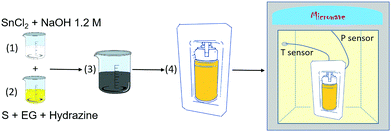 | ||
| Fig. 1 Diagram showing the synthesis procedure of the Sn1−δS powder using the microwave-assisted method. | ||
The sintering of the material was performed using a DR. SINTER LAB Jr. sps-212Lx spark plasma sintering (SPS) instrument at 450 °C and 50 MPa for 5 min within an 8 mm diameter graphite die. In this process, the Joule heating effect is concentrated in the interfaces of the grains, resulting in the sintering of the surfaces of the particles, while the bulk is exposed to minimal thermal effects.58 For this reason, the microstructure of the sample is maintained, thus avoiding a relevant increase in the particle size, although high-density pellets are achieved.
Characterization
Phase characterization was carried out by X-ray powder diffraction (XRPD) on an X’Pert PRO Alpha-1 Panalytical B.V. diffractometer with Cu Kα1 monochromatic radiation (λ = 1.54056 Å) at room temperature and at 650 °C in a 0.5 mm diameter quartz capillary. The capillary was previously charged with the microwave-synthesized tin sulphide powder in a glove box to avoid any possible oxidation during heating. Neutron powder diffraction (NPD) data were also collected at room temperature in the D2B beamline at the Institut Laue Langevin (ILL), Grenoble, using a radiation of 1.549 Å. This technique facilitates the decoupling of the thermal parameters and the occupancy, as there is a noteworthy difference in the neutron scattering lengths of the components of the sample [Sn (6.225 fm), S (2.847 fm)].59 Furthermore, neutron diffraction minimizes the preferred orientation effect, which sometimes is remarkable in a 2D material due to the packing of the ground powder in a cylindrical vanadium can. The NPD data were collected in the high-intensity mode for 1 g of the sample.The FullProf program60 was used to analyze the XRPD and NPD data by Rietveld refinement. A pseudo-Voigt function (a convolution of Gaussian and Lorentzian functions) was used to describe the profile of the diffraction peaks. A complete analysis was carried out by refining the scale factor, background coefficients, zero-point error, asymmetry, lattice parameters, atomic positions, occupancy (occ) and isotropic thermal parameters (Biso) for Sn and S.
The differential scanning calorimetry (DSC) analysis was performed in a TA Instruments Q600 with a 20 mg sample from room temperature to 800 °C under Argon flow at a heating rate of 5 °C min−1.
High resolution transmission electron microscopy (HRTEM) was carried out on a JEOL 3000F microscope (resolution 1.7 Å). For the microscopy study, the sample was ground in n-butyl alcohol and ultrasonically dispersed. A drop of the suspension was placed on a carbon-coated copper grid. The DigitalMicrograph package was utilized to obtain the Fast Fourier transforms (FFTs) of the HRTEM images.
Scanning electron microscope (SEM) images were acquired on a JEOL 6400 JSM after coating of the sample with gold. This microscope is equipped with an EDAX Inc. energy-dispersive X-ray detector for microanalysis.
A commercial MMR Technologies system was used to determine the Seebeck coefficient. Measurements were performed under vacuum (10−3 mbar) from room temperature to 800 K. A constantan wire was used as the reference for comparison with a bar-shaped sample of the material sintered by SPS, which was previously cut with a diamond saw perpendicular to the pressing direction. Electrical resistivity was measured in the same temperature range by using the van der Pauw measurement method.
Hall carrier concentration was measured by using the ac transport option of the Physical Properties Measurement System (PPMS) by Quantum Design. The measurement was carried out at a pressure of 10−5![[thin space (1/6-em)]](https://www.rsc.org/images/entities/char_2009.gif) Torr in the temperature range of 240–390
Torr in the temperature range of 240–390![[thin space (1/6-em)]](https://www.rsc.org/images/entities/char_2009.gif) K. The Hall carrier concentrations of the charge carriers (nH) were calculated using the Hall coefficient (RH) through the relation nH =
K. The Hall carrier concentrations of the charge carriers (nH) were calculated using the Hall coefficient (RH) through the relation nH = ![[thin space (1/6-em)]](https://www.rsc.org/images/entities/char_2009.gif) 1/RH·e, where e is the elementary charge.
1/RH·e, where e is the elementary charge.
Total thermal conductivity was determined from the thermal diffusivity (α) by using Linseis LFA equipment: κ = αCpd, where Cp is the specific heat and d is the sample density. The specific heat of the sample was calculated by using the Dulong–Petit approach. A thin graphite coating was applied to the surface of the pellet to maximize heat absorption and emissivity.
Results and discussion
Structural and microstructural characterization
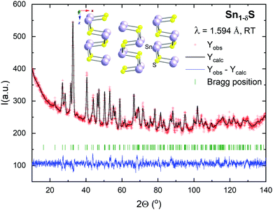
Fig. 2 shows the Rietveld refinement of the neutron powder diffraction (NPD) data and the crystal structure representation at room temperature. The structure was refined in the orthorhombic Pnma space group (No. 62) with unit-cell parameters a = 11.1966(2) Å, b = 3.9847(6) Å and c = 4.3272(6) Å, and V = 193.06(1) Å3. These values are in good agreement with those reported in the Inorganic Crystal Structure Database for stoichiometric SnS (a = 11.200 Å, b = 3.987 Å and c = 4.334 Å, and V = 193.53 Å3).61 Both Sn and S atoms are located at the 4c Wyckoff position. The occupancy factor of Sn (with S fixed to unity) is 0.87(1), indicating a notable presence of Sn vacancies, randomly distributed in the structure. This non-stoichiometric compound is the result of the synthesis under the conditions described in the experimental section. There is just a slight contraction in the unit-cell volume deriving from the presence of Sn vacancies, since this effect is probably offset by the repulsion of the anion sublattice in the resulting voids. Previous results in the literature suggest that these vacancies have a strong influence on the transport properties of the material; the composition is optimized for thermoelectric applications when the Sn content is between 0.8 and 0.9.38 The atomic positions, isotropic thermal parameters, occupancy, characteristic bond angles and distances, at room temperature, determined from the Rietveld refinement, are presented in Table 1. The structure consists of puckered layers of SnS3 pyramids (Sn–S: 2.65–2.69 Å) sharing vertices, with an important interlayer space (Sn–S: 3.34 Å) that confers 2D-like properties to this material, accounting for the easiness for exfoliation.| x | y | z | B iso (Å2) | Occ | |
|---|---|---|---|---|---|
| Sn | 0.1174(2) | 0.25 | 0.1194(6) | 0.27(4) | 0.87(1) |
| S | 0.1482(5) | 0.75 | 0.5295(9) | 0.74(4) | 1 |
| Characteristic bond distances (Å) and angles (°) from NPD data | |||||
| Sn–S | 2.652(6) | 2.690 (3) × 2 | |||
| Sn–S (interlayer) | 3.340(4) | ||||
| S–Sn–S | 95.58(3) | 89.38 (3) × 2 | |||
| Sn–S–Sn | 95.58(3) | 102.58 (3) × 2 | |||
The structure determined through the NPD experiment was supported by the HRTEM results. As an example, Fig. 3 shows the HRTEM micrograph taken along the [100] and [001] zone axes. The image shows a well-ordered crystal structure. This is indicated by the absence of extra reflections or streaking in the FFTs displayed in the insets of Fig. 3. The black dots indicate the projections of the atomic columns. In the HRTEM image, it is possible to measure directly the a, b and c cell parameters, which correspond to 11.2, 3.9 and 4.3 Å, respectively. These values are consistent with those measured by NPD.
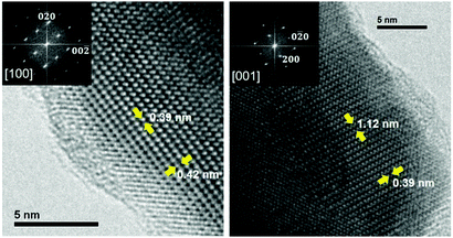 | ||
| Fig. 3 Experimental HRTEM micrographs along the [100] and [001] zone axes. FFT images are shown in the insets. | ||
The DSC analysis for the sample upon heating and cooling is presented in Fig. 4. An endothermic peak with a minimum at 618 °C appears during heating, while in the cooling run there is an exothermic signal with noticeable hysteresis and a maximum at 584 °C. Similar to the result for analogous SnSe, the difference in the heat flow can be attributed to the reversible Pnma–Cmcm transition.62
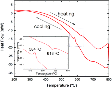 | ||
| Fig. 4 DSC analysis in argon for microwave-hydrothermal-synthesized Sn1−δS in two consecutive heating and cooling cycles. | ||
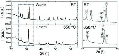
In order to confirm this transition, we have performed temperature-dependent laboratory XRPD in a 0.5 mm diameter quartz capillary. Fig. 5 displays the X-ray diffractogram of the sample at room temperature and above the transition temperature determined by the DSC analysis. The unit-cell parameters for the Cmcm phase at 650 °C were found to be a = 4.117(1) Å, b = 11.392(3) Å and c = 4.127(2) Å.
Fig. 6a shows the SEM image of the Sn1−δS powder. A plate-like microstructure is perceptible in the micrograph. The crystals possess a thickness from 100 nm to 500 nm and a length of about 3–4.5 μm. The microstructure is preserved after the SPS sintering of the powder (Fig. 6b), containing the randomly oriented platelets. However, as it can be observed in the micrograph for the cross-section of the pellet, there is a high degree of compaction, which facilitates the appropriate measurement of the thermoelectric properties. The density of the pellet was geometrically estimated to be in the range of ≈94 ± 5% of the theoretical density (5.3 g cc−1). The semi-quantitative EDAX analysis of 20 different points in the powder sample and in the SPS processed pellet indicates a similar atomic percentage, within the error of this method, which is 45% for Sn and 55% for S in the powder, and 46% for Sn and 54% for S in the sintered material.
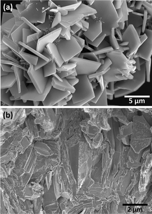 | ||
| Fig. 6 SEM micrograph of Sn1−δS: (a) powder synthesized by the microwave-hydrothermal method and (b) the cross-section of the SPS sintered pellet. | ||
Thermoelectric properties
Fig. 7 shows the electrical properties of the Sn1−δS sample obtained by microwave-hydrothermal synthesis. The positive value of the Seebeck coefficient (Fig. 7a) reveals dominant hole conduction (p-type semiconductor) throughout the studied temperature range. The Seebeck coefficient value increases from 591 μV K−1 at room temperature to 710 μV K−1 at 423 K. It then slightly drops at higher temperatures. This small reduction of the Seebeck coefficient at high temperatures was previously described as an effect of the thermal excitation of minority carriers, i.e. bipolar effect.63 It has been shown in other chalcogenides that energy filtering by potential barriers may occur in nanocomposites.64 This effect increases the Seebeck coefficient by removing the contribution of low energy electrons and is usually more intense at fairly low temperatures. Therefore, energy filtering in grain boundaries can explain the higher maximum thermopower at lower temperatures than those reported previously.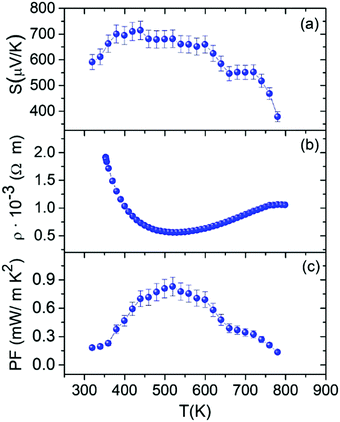 | ||
| Fig. 7 Temperature dependence of the (a) Seebeck coefficient, (b) electrical resistivity and (c) power factor of Sn1−δS synthesized using the microwave-hydrothermal method. | ||
Considering the maximum value of the Seebeck coefficient found for Sn1−δS synthesized by microwave irradiation, it is possible to estimate the energy band gap (Eg) of the material, using the Goldsmid–Sharp equation (eqn (2)).
| Eg = |Smax|2eTmax | (2) |
In this equation, e corresponds to the elementary charge and Tmax is the temperature at which the maximum of the Seebeck coefficient (Smax) occurs. The approximation of the energy band gap (Eg) for this sample gives a value of 0.63 eV. The error in the calculation when using this approach is up to 20% of the determined value.65 However, it is understandable that this value is much lower than the one calculated for the stoichiometric SnS compound in the Pnma space group (≈0.95 eV).66 This is a clear indication of the effect of Sn vacancies on the electronic properties of the microwave-synthesized sample.67
The temperature dependence of the electrical resistivity is shown in Fig. 7b. First, the electrical resistivity of the sample decreases from 1.9 × 10⁻³ Ω m at room temperature to 5.6 × 10⁻⁴ Ω m at 529 K. Then, there is a smooth increment in the electrical resistivity to 780 K, and finally it is slightly reversed at higher temperatures. This behavior found for this sample is similar to that described for SnSe, where a phonon scattering mechanism dominates the transport properties at high temperatures but grain boundary potential barrier scattering limits the carrier mobility at low temperatures.68,69
The power factor (PF = S2/ρ) of Sn1−δS (Fig. 7c) was determined from the measured Seebeck coefficient and electrical resistivity. The large Seebeck coefficient helps improve the power factor, reaching the value of 0.83 mW m−1 K−2 at 519 K.
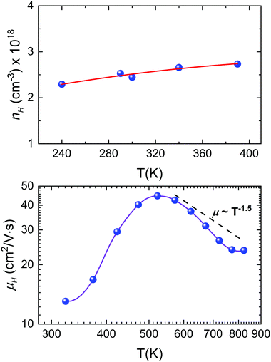
The temperature dependence of the Hall carrier concentration is shown in Fig. 8a. At room temperature, microwave-synthesized Sn1−δS shows a carrier density around 2.5 × 1018 cm−3. This value is considerably higher than the values reported for pristine SnS prepared by ball-milling, with values around 8 × 1016 cm−3 (Z. Wang et al.)70 or 1 × 1015 cm−3 (Q. Tan et al.).71 In fact, due to the Sn vacancies, our sample shows a carrier density analogous to that of Ag-doped compounds.71,72 In addition, by considering the large effect of the Sn vacancies over the Seebeck coefficient, discussed above, this nH value could be more easily tuned through adequate doping in order to obtain an optimum thermoelectric performance.
The temperature dependence of mobility for Sn1−δS is shown in Fig. 8b, which is 13 cm2 V−1 s−1 at room temperature. This mobility is more than twice that reported for pristine SnS, with values around 6 cm2 V−1 s−1, and shows an even greater difference if we compare it with the mobility reported for Ag-doped SnS, which varies between 5 and 2 cm2 V−1 s−1 depending on the amount of tin vacancies.71,72 The mobility increases with temperature, reaching 45 cm2 V−1 s−1 at 523 K, and then decreases down to ∼24 cm2 V−1 s−1 at 800 K. This change in the slope is associated with a variation in the scattering mechanism and it has been already reported for other doped tin sulphides.69,72 A useful strategy to understand the scattering mechanism that is applied here is to analyze the scattering factor p via μH ∼ Tp. Above 550 K, the Hall mobility shows an approximate μH ∼ T−1.5 temperature dependence. This corresponds to charge carrier scattering dominated by acoustic phonons and it has been observed already in SnS with Na-doping.69
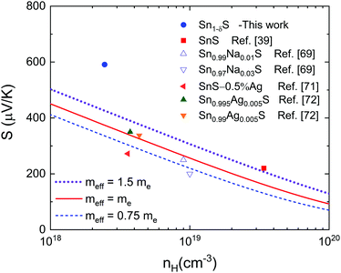
Fig. 9 shows the Pisarenko plot calculation applying the single parabolic band (SPB) model and assuming carrier scattering dominated by acoustic phonons (ESI,‡ eqn (S2)).73,74 Although SnS crystals show a complex three-valence-band transport feature,39 this model has already been successfully applied to polycrystalline SnS samples.69,72 The model, as applied here, includes the influence of band degeneracy within the effective mass (meff), i.e. the apparent mass of the charge carriers in the material compared to that in a vacuum. If the band degeneracy were known, some intuition about the actual band mass could be gained. This meff is usually presented as a quantity proportional to the electron mass, me. Moreover, this meff is related to the density of states band mass mDOSvia (meff)3/2 = Nv(mDOS)3/2, where Nv is the number of equivalent valleys in the electronic band structure. Shown by other chalcogenides, the outlier value reported here can be explained as a consequence of the low energy electron filtering.64 Although our measured carrier density is lower than that reported for the single crystal compound, it is higher, as mentioned earlier, than the reported values for pristine polycrystalline SnS71 and similar to other ones found in the literature for doped polycrystalline SnS.69,71
Clearly the SPB model is inadequate to describe the electronic properties of microwave synthesized SnS, since the Seebeck coefficient is almost 50% higher for the same charge carrier density than the projection, even with an unrealistically large assumed effective mass. We may recall from the above the estimated band-gap of 0.63 eV, which is considerably below the accepted 0.95 eV for SnS66 due to the significant Sn deficiency. The Sn deficiency can induce a so-called broad defect-band above the valence band, at least for the sister compound SnSe, according to ab initio calculations.67 This would explain the reduced band-gap, the higher values of nH and meff and the enlarged Seebeck coefficient.
The total thermal conductivity (Fig. 10a), dominated by the lattice thermal conductivity, can be analyzed in terms of the Callaway model (Fig. 10b, with details in the ESI‡). At room temperature, we found a value of 1.0 W m−1 K−1. The fit using the Callaway model agrees well with the measured data, and the fitted parameters suggest predominant phonon scattering due to Umklapp processes in this material at high temperatures, which is also corroborated by the observed ∼T−1 decrease.75 The slight jump observed at ∼550 K occurs at the same temperature where the maximum mobility is reached, so it is also probably related to a change in the scattering mechanism.69
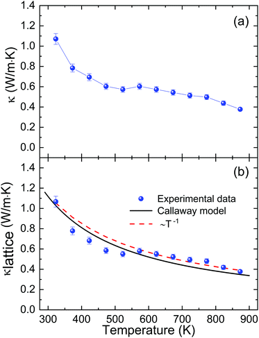 | ||
| Fig. 10 Temperature dependence of the (a) total thermal conductivity and (b) lattice thermal conductivity of microwave-synthesized Sn1−δS. The black solid line represents the data calculated using the Callaway model,76 while the dotted line shows the ∼T−1 fit. | ||
The temperature dependence of the figure of merit ZT of the sample is shown in Fig. 11. The reasonably high power factor, combined with the intrinsically low thermal conductivity, produces a ZT value of 0.76 at 523 K. This value is similar to that reported by Yang et al.38 for the Sn0.8S and Sn0.85S samples (ZT ≈ 0.8) and higher than the values reported by Zhou et al. (ZT ≈ 0.65),69 Asfandiyar et al. (ZT ≈ 0.21),72 W.-D. Liu et al. (ZT ≈ 0.2)77 and Y. M. Han et al. (ZT ≈ 0.18)78 for SnS polycrystalline samples. However, there is still room for improvement in the thermoelectric performance of this system. This is evidenced by the recent work on the synthesis by ball-milling of Sn0.99Ag0.005S.72 The enhancement of the charge carrier concentration by Ag-doping and the vacancy engineering produces a maximum value of ZT ≈ 1.1 at 877 K. Even more impressive is the result found by He et al.39 for the SnS0.91Se0.09 crystals. A ZTaverage value of 1.25 was measured in the temperature range from 300 K to 873 K.
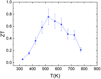 | ||
| Fig. 11 Temperature dependence of the figure of merit (ZT) for Sn1−δS synthesized using the microwave-hydrothermal method. | ||
In summary, Table 2 shows the thermoelectric properties of some representative SnS-based compounds from the literature. The indicated values are an approximation, extracted from the graphs of some selected publications (references included in the last column of the table), which provide a comparison with the microwave-synthesized Sn1−δS sample. The Seebeck coefficient, electrical resistivity and thermal conductivity values are given for the ZTmax temperature, while the carrier concentration and mobility values are indicated at 300 K.
| Composition | ZT max | At ZTmax temperature | At 300 K | Ref. | |||
|---|---|---|---|---|---|---|---|
| S (μV K−1) | ρ (Ω m) | κ (W m−1 K−1) | n H (cm−3) | μ H (cm2 V−1 s−1) | |||
| Sn0.87S (this work) | 0.76 | 682 | 5.6 × 10⁻⁴ | 0.57 | 2.5 × 10¹⁸ | 13.0 | — |
| SnS | 0.25 | 425 | 7.1 × 10⁻⁴ | 0.70 | 8.0 × 10¹⁶ | 0.3 | 70 |
| SnS | 0.18 | 680 | 5.1 × 10⁻² | 0.45 | 2.0 × 10¹⁷ | 3.0 | 78 |
| SnS | 0.21 | 480 | 1.1 × 10⁻³ | 0.58 | — | — | 72 |
| SnS | 0.50 | 425 | 5.8 × 10⁻⁴ | 0.55 | 2.0 × 10¹⁸ | 2.5 | 38 |
| Sn0.8S | 0.80 | 360 | 2.7 × 10⁻⁴ | 0.53 | 8.0 × 10¹⁸ | 2.5 | 38 |
| Sn0.97Na0.03S | 0.60 | 380 | 3.7 × 10⁻⁴ | 0.60 | 3.1 × 10¹⁸ | 17.7 | 70 |
| Sn0.99Ag0.005S | 1.1 | 375 | 3.3 × 10⁻⁴ | 0.34 | 3.1 × 10¹⁸ | 5.3 | 72 |
Conclusions
High thermoelectric performance was found for microwave-hydrothermal-synthesized polycrystalline tin sulphide. Structural characterization through neutron powder diffraction reveals a significant amount of Sn vacancies in the structure, yielding a composition of Sn0.87S. These cation vacancies benefit the enhancement of the high carrier density and mobility, thus improving the power factor and decreasing the thermal conductivity. As a result, a figure of merit of 0.76 at 523 K is reached for the studied composition.Higher thermoelectric performance can be achieved by optimizing the charge carrier concentration, tuning the band structure of the material by suitable chemical doping and controlling the content of vacancies in the structure.
Conflicts of interest
There are no conflicts to declare.Acknowledgements
We are grateful to the Spanish Ministry of Economy and Competitiveness for granting the projects MAT2017-84496-R and MAT2017-87134-C2-2-R. J. P. G. thanks the Community of Madrid for granting the “Atracción de Talento program” fellowship (2017-T2/I ND-5597) and project PR65/19-22459. J. G. would like to acknowledge MICINN for granting the contract PRE2018-083398. We wish to express our gratitude to the ILL technical staff for making the facilities available for the neutron experiment, to the SPS service at ICMM-CSIC, to CAI Difracción de Rayos X and to Centro Nacional de Microscopía Electrónica (CNME) at the Universidad Complutense de Madrid (UCM).References
- R. Freer and A. V. Powell, J. Mater. Chem. C, 2020, 8, 441–463 RSC.
- M. Islam, M. Hasanuzzaman, A. Pandey and N. Rahim, Energy for Sustainable Development, Elsevier, 2020, pp. 19–39 Search PubMed.
- D. Beretta, N. Neophytou, J. M. Hodges, M. G. Kanatzidis, D. Narducci, M. Martin-Gonzalez, M. Beekman, B. Balke, G. Cerretti and W. Tremel, Mater. Sci. Eng., R, 2019, 138, 100501 CrossRef.
- L. Yang, Z. G. Chen, M. S. Dargusch and J. Zou, Adv. Energy Mater., 2018, 8, 1701797 CrossRef.
- C. Gayner and K. K. Kar, Prog. Mater. Sci., 2016, 83, 330–382 CrossRef CAS.
- M. Zebarjadi, K. Esfarjani, M. Dresselhaus, Z. Ren and G. Chen, Energy Environ. Sci., 2012, 5, 5147–5162 RSC.
- P. Vaqueiro and A. V. Powell, J. Mater. Chem., 2010, 20, 9577–9584 RSC.
- G. J. Snyder and E. S. Toberer, Materials for Sustainable Energy: A Collection of Peer-Reviewed Research and Review Articles from Nature Publishing Group, World Scientific, 2011, pp. 101–110 Search PubMed.
- M. H. Elsheikh, D. A. Shnawah, M. F. M. Sabri, S. B. M. Said, M. H. Hassan, M. B. A. Bashir and M. Mohamad, Renewable Sustainable Energy Rev., 2014, 30, 337–355 CrossRef.
- X. Zhang and L.-D. Zhao, J. Materiomics, 2015, 1, 92–105 CrossRef.
- J. R. Sootsman, D. Y. Chung and M. G. Kanatzidis, Angew. Chem., Int. Ed., 2009, 48, 8616–8639 CrossRef CAS PubMed.
- D. Wright, Nature, 1958, 181, 834 CrossRef.
- M. Scheele, N. Oeschler, K. Meier, A. Kornowski, C. Klinke and H. Weller, Adv. Funct. Mater., 2009, 19, 3476–3483 CrossRef CAS.
- J. P. Heremans, V. Jovovic, E. S. Toberer, A. Saramat, K. Kurosaki, A. Charoenphakdee, S. Yamanaka and G. J. Snyder, Science, 2008, 321, 554–557 CrossRef CAS PubMed.
- J. Gainza, F. Serrano-Sánchez, N. Biskup, N. M. Nemes, J. L. Martínez, M. T. Fernández-Díaz and J. A. Alonso, Materials, 2019, 12, 3783 CrossRef CAS PubMed.
- E. K. Lee, L. Yin, Y. Lee, J. W. Lee, S. J. Lee, J. Lee, S. N. Cha, D. Whang, G. S. Hwang and K. Hippalgaonkar, Nano Lett., 2012, 12, 2918–2923 CrossRef CAS PubMed.
- N. Mingo, D. Hauser, N. Kobayashi, M. Plissonnier and A. Shakouri, Nano Lett., 2009, 9, 711–715 CrossRef CAS PubMed.
- F. Serrano-Sánchez, M. Funes, N. M. Nemes, O. J. Dura, J. L. Martínez, J. Prado-Gonjal, M. T. Fernández-Díaz and J. A. Alonso, Appl. Phys. Lett., 2018, 113, 083902 CrossRef.
- S. Perumal, S. Roychowdhury and K. Biswas, J. Mater. Chem. C, 2016, 4, 7520–7536 RSC.
- S. M. Kauzlarich, S. R. Brown and G. J. Snyder, Dalton Trans., 2007, 2099–2107 RSC.
- E. S. Toberer, A. F. May and G. J. Snyder, Chem. Mater., 2009, 22, 624–634 CrossRef.
- M. Fedorov, J. Thermoelectr., 2009, 2, 51–60 Search PubMed.
- C. B. Vining, CRC Handbook of Thermoelectrics, 1995, 1, pp. 329–337 Search PubMed.
- C. Uher, Semiconductors and Semimetals, Elsevier, 2001, vol. 69, pp. 139–253 Search PubMed.
- B. Sales, D. Mandrus and R. K. Williams, Science, 1996, 272, 1325–1328 CrossRef CAS PubMed.
- F. Serrano-Sánchez, J. Prado-Gonjal, N. M. Nemes, N. Biskup, M. Varela, O. J. Dura, J. L. Martínez, M. T. Fernández-Díaz, F. Fauth and J. A. Alonso, J. Mater. Chem. A, 2018, 6, 118–126 RSC.
- C. Fu, S. Bai, Y. Liu, Y. Tang, L. Chen, X. Zhao and T. Zhu, Nat. Commun., 2015, 6, 8144 CrossRef PubMed.
- H. Xie, H. Wang, Y. Pei, C. Fu, X. Liu, G. J. Snyder, X. Zhao and T. Zhu, Adv. Funct. Mater., 2013, 23, 5123–5130 CrossRef CAS.
- T. Zhu, C. Fu, H. Xie, Y. Liu and X. Zhao, Adv. Energy Mater., 2015, 5, 1500588 CrossRef.
- J.-A. Dolyniuk, B. Owens-Baird, J. Wang, J. V. Zaikina and K. Kovnir, Mater. Sci. Eng., R, 2016, 108, 1–46 CrossRef.
- B. B. Iversen, A. E. Palmqvist, D. E. Cox, G. S. Nolas, G. D. Stucky, N. P. Blake and H. Metiu, J. Solid State Chem., 2000, 149, 455–458 CrossRef CAS.
- L.-D. Zhao, S.-H. Lo, Y. Zhang, H. Sun, G. Tan, C. Uher, C. Wolverton, V. P. Dravid and M. G. Kanatzidis, Nature, 2014, 508, 373 CrossRef CAS PubMed.
- Z.-G. Chen, X. Shi, L.-D. Zhao and J. Zou, Prog. Mater. Sci., 2018, 97, 283–346 CrossRef CAS.
- Y. K. Lee, Z. Luo, S. P. Cho, M. G. Kanatzidis and I. Chung, Joule, 2019, 3, 719–731 CrossRef CAS.
- L.-D. Zhao, C. Chang, G. Tan and M. G. Kanatzidis, Energy Environ. Sci., 2016, 9, 3044–3060 RSC.
- U. Aseginolaza, R. Bianco, L. Monacelli, L. Paulatto, M. Calandra, F. Mauri, A. Bergara and I. Errea, Phys. Rev. B, 2019, 100, 214307 CrossRef CAS.
- S. Hao, V. P. Dravid, M. G. Kanatzidis and C. Wolverton, APL Mater., 2016, 4, 104505 CrossRef.
- H. Q. Yang, X. Y. Wang, H. Wu, B. Zhang, D. D. Xie, Y. J. Chen, X. Lu, X. D. Han, L. Miao and X. Y. Zhou, J. Mater. Chem. C, 2019, 7, 3351–3359 RSC.
- W. He, D. Wang, H. Wu, Y. Xiao, Y. Zhang, D. He, Y. Feng, Y.-J. Hao, J.-F. Dong, R. Chetty and L.-D. Zhao, Science, 2019, 365, 1418–1424 CrossRef CAS PubMed.
- A. V. Powell and P. Vaqueiro, Thermoelectric Materials and Devices, 2016, p. 27 Search PubMed.
- J. Prado-Gonjal, P. Vaqueiro, C. Nuttall, R. Potter and A. V. Powell, J. Alloys Compd., 2017, 695, 3598–3604 CrossRef CAS.
- F. Serrano-Sánchez, M. Gharsallah, N. Nemes, N. Biskup, M. Varela, J. Martínez, M. Fernández-Díaz and J. Alonso, Sci. Rep., 2017, 7, 6277 CrossRef PubMed.
- F. Serrano-Sánchez, M. Gharsallah, J. Bermúdez, F. Carrascoso, N. M. Nemes, O. J. Dura, M. A. L. de la Torre, J. L. Martínez, M. T. Fernández-Díaz and J. A. Alonso, Thermoelectrics for Power Generation-A Look at Trends in the Technology, 2016 Search PubMed.
- F. Serrano, M. Gharsallah, W. Cherif, J. L. Martinez, V. Cascos, L. Troncoso and J. A. Alonso, Mater. Today: Proc., 2015, 2, 661–668 Search PubMed.
- J. Prado-Gonjal, F. Serrano-Sánchez, N. M. Nemes, O. J. Dura, J. L. Martínez, M. T. Fernández-Díaz, F. Fauth and J. A. Alonso, Appl. Phys. Lett., 2017, 111, 083902 CrossRef.
- B. Poudel, Q. Hao, Y. Ma, Y. Lan, A. Minnich, B. Yu, X. Yan, D. Wang, A. Muto and D. Vashaee, Science, 2008, 320, 634–638 CrossRef CAS PubMed.
- K. Biswas, S. Muir and M. A. Subramanian, Mater. Res. Bull., 2011, 46, 2288–2290 CrossRef CAS.
- E. Savary, F. Gascoin and S. Marinel, Dalton Trans., 2010, 39, 11074–11080 RSC.
- Y. Li, C. Cheng, Y. Lei, M. Wang and R. Wan, Dalton Trans., 2017, 46, 33–38 RSC.
- J. Prado-Gonjal, R. Schmidt and E. Morán, Inorganics, 2015, 3, 101–117 CrossRef CAS.
- G. Cravotto and D. Carnaroglio, Microwave Chemistry, De Gruyter, Berlin, Germany, 2017 Search PubMed.
- R. Schmidt, J. Prado-Gonjal and E. Morán, CRC concise encyclopedia of nanotechnology, CRC Press Taylor & Francis Group, Boca Raton (USA), 2015 Search PubMed.
- P. Pichanusakorn and P. Bandaru, Mater. Sci. Eng., R, 2010, 67, 19–63 CrossRef.
- M. G. Kanatzidis, Chem. Mater., 2009, 22, 648–659 CrossRef.
- J. P. Heremans, M. S. Dresselhaus, L. E. Bell and D. T. Morelli, Nat. Nanotechnol., 2013, 8, 471 CrossRef CAS PubMed.
- Y. Pei, X. Shi, A. LaLonde, H. Wang, L. Chen and G. J. Snyder, Nature, 2011, 473, 66 CrossRef CAS PubMed.
- J. Prado-Gonjal, R. Heuguet, D. Muñoz-Gil, A. Rivera-Calzada, S. Marinel, E. Morán and R. Schmidt, Int. J. Hydrogen Energy, 2015, 40, 15640–15651 CrossRef CAS.
- G. Sweet, M. Brochu, R. Hexemer Jr, I. Donaldson and D. Bishop, Mater. Sci. Eng., A, 2014, 608, 273–282 CrossRef CAS.
- V. F. Sears, Neutron news, 1992, 3, 26–37 CrossRef.
- J. Rodríguez, Commission on Powder Diffraction (IUCr), Newsletter, 2001, 26, 12–19 Search PubMed.
- H. Wiedemeier, H. Georg and G. von Schnering, Z. Kristallogr. Cryst. Mater., 1978, 148, 295–304 CrossRef CAS.
- F. Serrano-Sánchez, N. M. Nemes, O. J. Dura, M. T. Fernandez-Diaz, J. L. Martínez and J. A. Alonso, J. Appl. Crystallogr., 2016, 49, 2138–2144 CrossRef.
- D. Feng, Z.-H. Ge, D. Wu, Y.-X. Chen, T. Wu, J. Li and J. He, Phys. Chem. Chem. Phys., 2016, 18, 31821–31827 RSC.
- C. Gayner and Y. Amouyal, Adv. Funct. Mater., 2019, 1901789 Search PubMed.
- H. Goldsmid and J. Sharp, J. Electron. Mater., 1999, 28, 869–872 CrossRef CAS.
- K. Persson, Materials Data on SnS (SG: 62) by Materials Project, LBNL Materials Project, Lawrence Berkeley National Lab.(LBNL), Berkeley, CA, 2016 Search PubMed.
- J. Gainza, F. Serrano-Sánchez, M. Gharsallah, F. Carrascoso, J. Bermúdez, O. Dura, F. J. Mompean, N. Biskup, J. Meléndez, J. Martínez, J. A. Alonso and N. M. Nemes, J. Appl. Phys., 2019, 126, 045105 CrossRef.
- D. Feng, Z.-H. Ge, Y.-X. Chen, J. Li and J. He, Nanotechnology, 2017, 28, 455707 CrossRef PubMed.
- B. Zhou, S. Li, W. Li, J. Li, X. Zhang, S. Lin, Z. Chen and Y. Pei, ACS Appl. Mater. Interfaces, 2017, 9, 34033–34041 CrossRef CAS PubMed.
- Z. Wang, D. Wang, Y. Qiu, J. He and L.-D. Zhao, J. Alloys Compd., 2019, 789, 485–492 CrossRef CAS.
- Q. Tan, L.-D. Zhao, J.-F. Li, C.-F. Wu, T.-R. Wei, Z.-B. Xing and M. G. Kanatzidis, J. Mater. Chem. A, 2014, 2, 17302–17306 RSC.
- Asfandiyar, B. Cai, L.-D. Zhao and J.-F. Li, J. Materiomics, 2020, 6, 77–85 CrossRef.
- A. F. May, E. S. Toberer, A. Saramat and G. J. Snyder, Phys. Rev. B: Condens. Matter Mater. Phys., 2009, 80, 125205 CrossRef.
- A. F. May and G. J. Snyder, Materials, preparation, and characterization in thermoelectrics, CRC press, 2017, pp. 11–18 Search PubMed.
- M. Jin, Z. Chen, X. Tan, H. Shao, G. Liu, H. Hu, J. Xu, B. Yu, H. Shen and J. Xu, ACS Energy Lett., 2018, 3, 689–694 CrossRef CAS.
- J. Callaway, Phys. Rev., 1959, 113, 1046 CrossRef CAS.
- W.-D. Liu, X.-L. Shi, Z.-J. Lin, Q. Sun, G. Han, Z.-G. Chen and J. Zou, ACS Appl. Energy Mater., 2020, 3, 2192–2199 CrossRef CAS.
- Y.-M. Han, J. Zhao, M. Zhou, X.-X. Jiang, H.-Q. Leng and L.-F. Li, J. Mater. Chem. A, 2015, 3, 4555–4559 RSC.
Footnotes |
| † This paper is dedicated to the memory of our colleague and friend Professor Emilio Morán. We will always remember your smile and big heart. You will be always in our thoughts. |
| ‡ Electronic supplementary information (ESI) available: Pisarenko line and Lorenz number; modeling of lattice thermal conductivity. See DOI: 10.1039/d0ma00301h |
| This journal is © The Royal Society of Chemistry 2020 |

