Fullerenes: the stars of photovoltaics
Silvia
Collavini
 *a and
Juan Luis
Delgado
 *ab
*ab
aPOLYMAT, University of the Basque Country UPV/EHU, Faculty of Chemistry, Avenida de Tolosa 72, P. Manuel Lardizabal 3, Donostia – San Sebastián, Spain. E-mail: silvia.collavini@polymat.eu
bIkerbasque, Basque Foundation for Science, 48011 Bilbao, Spain. E-mail: juanluis.delgado@polymat.eu
First published on 21st June 2018
Abstract
“The molecule, buckminsterfullerene, is beautiful physically and intellectually. Its qualities, and even some of its properties, can be appreciated instantly and intuitively by nonscientists. Its uniqueness is bound to lead to novel applications – superconductivity is the leading contender at the moment”. So the journalist Hugh Aldersey-Williams presented in his book about C60 fullerene, “The Most Beautiful Molecule”, first published in 1995. Despite being quite old, this sentence is still strongly valid. In fact, since their discovery in 1985, fullerenes have raised huge interest among the scientific community, and they still preserve and increase it. This resulted in an impressive amount of research dealing with the molecule and its derivatives, and most of these studies have been collected in numerous reviews concerning fullerene's various properties and applications. Precisely due to the existence of these uncountable reviews, the present paper will take a slightly different path by describing important facts about fullerenes in the field of photovoltaics.
Introduction
The discovery of C60 fullerene in 1985 by Harold W. Kroto, Richard E. Smalley, and Robert F. Curl was a breakthrough in scientific research.1 These scientists received the Nobel Prize in 1996 in recognition of their amazing discovery, which revolutionised chemistry and all the fields that took advantage of fullerene's versatility.2Interestingly, other researchers predicted the possible existence of these novel carbon allotropes earlier. David Jones in 1966 under the pseudonym of Daedalus wrote: “The high-temperature graphite production might be modified to generate graphite balloons”.3,4
Four years later, Eiji Osawa reported his conjecture on the existence of a C60 molecule, whose structure was inspired by the symmetry of a modern soccer ball.5 The theory of Osawa was followed by the first Hückel calculations confirming his hypotheses.6,7 Indeed, R. A. Davidson wrote in 1981 “The (non-platonic) truncated icosahedron graph (…) corresponds to the hypothetical molecule C60, a spheroidal, polyhedral oligomer of carbon and formally a trimer of bowl-shaped corannulene”. The Schlegel map of this truncated icosahedron can be seen in Fig. 1.
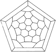 | ||
| Fig. 1 Z2 automorphism reduction of the truncated icosahedron, IVl = 60 reprinted from ref. 7 with permission of Springer Nature. | ||
However, the most important step in the search for fullerenes took place at Rice University, Houston, Texas. After the laser irradiation of graphite under an inert atmosphere, the mass spectra registered intense peaks at 720 a.m.u., corresponding to 60 carbon atoms (C60) and a less intense peak at 840 a.m.u. (C70). There were numerous hypotheses and viewpoints concerning the most likely structure of C60, which are explained in two interesting and catchy articles, “C60: Buckminsterfullerene, The Celestial Sphere that Fell to Earth” by Harold Kroto and “Great Balls of Carbon” by Richard Smalley.8,9 Considering both the titles of Kroto's paper and the present work, it is nice to explain this word choice by pointing out how stars are a leitmotiv of the fullerene history: first discovered by recreating the environment of a star, fullerene is now a protagonist of research which aims to obtain energy from our star, the sun.
Initially, the molecule was named buckminsterfullerene, in honour of Richard Buckminster Fuller, the designer of a geodesic dome that resembles the structure of the molecule.10 To illustrate the impact of the discovery of C60, it is worth mentioning that Texas (USA) is the first state to designate a molecule as an official state symbol: precisely, C60 fullerene.11
Since the conditions of the experiments that led to the final discovery of fullerene recreated the atmosphere of a carbon star, it was speculated that fullerenes could be found in outer space and maybe also on our planet, coming from meteorites. It is logical to assume that the laboratory conditions required for the formation of fullerenes are quite drastic, making the possibility of a natural formation of these molecules rather difficult.
In 1992, some traces of fullerite (the mineral form of fullerene) were found in shungite, a carbonaceous rock which is supposed to be Precambrian, but whose features make it difficult to be properly classified.12 This finding indicates that fullerenes might also be highly stable with respect to time, in addition to their known stability to temperature and pressure.13
Since the very moment of its discovery, C60 has been the subject of countless studies thanks to its interesting properties. In fact, due to its unique structure, this astonishing molecule can accept and transfer electrons,14–18 it is able to accommodate inside its cage small structures such as metals (endohedral fullerenes),19,20 and it can be functionalized on the surface through several reactions. Thanks to its rich chemical versatility, it is possible to get derivatives that have a wide range of potential applications, for example in biomedicine, where they can act as drug carriers or MRI contrast agents.21–24 Undoubtedly, the field where fullerenes have demonstrated the highest feasibility and appeal is photovoltaics, both in organic photovoltaics (OPVs) and in perovskite solar cells (PSCs). Being able to transfer electrons in such an efficient way might be the most fascinating feature of fullerenes: the charge mobility of C60 and its derivatives is generally on the order of 10−4 to 10−3 cm2 (V s)−1.25 Theoretical studies have tried to better explain this behaviour, which may be ascribable to the peculiar hybridization of the carbon atoms of C60.14 Due to the curvature imposed by the cage and the pentagons, the hybridization is suspected to be a mixture of sp2, typical of graphite, and sp3, typical of diamond. At this point, it is relevant to highlight why fullerenes are preferable with respect to other carbon nanomaterials. Carbon nanotubes, for example, have been studied for applications in OPV, but present one major drawback: an average batch of single-wall carbon nanotubes (SWCNTs) contains both metallic (∼33%) and semiconducting SWCNTs (∼66%). The difference between the two types of CNTs lies in the chirality. The problem with the mixture is that metallic SWCNTs tend to favour charge recombination, thus hindering a good device performance.26,27
The intermediate nature of fullerene hybridization means that it can also be varied; rehybridization seems to play an important role in the electronic structure and thus in the electron-accepting ability of the C60 cage.
In addition, fullerenes possess low reorganization energy and have been demonstrated to be able to slow down charge recombination in the dark.28
Thanks to all these useful properties, C60 and major fullerenes have been widely used in photovoltaics, both in their pristine and functionalized forms.29,30 There are already very interesting review articles on fullerene-based photovoltaics addressing its use in OPVs as well as in PSCs.29–36 In the present review article we would like to show the most peculiar and interesting discoveries concerning fullerenes in photovoltaics, specifically those examples which afforded new knowledge and understanding, and contributed to major advances in this field.
Fullerenes for organic photovoltaics
OPVs: an introduction
The mechanism of operation of OPVs starts upon sunlight absorption by electron donor molecules to generate relatively localized excited states.37,38 The so-generated excitons migrate towards the donor–acceptor interface (p/n junctions), where they dissociate into positive and negative charges, which are transported towards the electrodes, where they are collected. The most used architecture of these kinds of cells, known as bulk heterojunction solar cells, is shown in Fig. 2.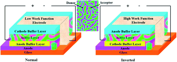 | ||
| Fig. 2 Configurations of normal and inverted bulk heterojunction organic solar cells. Reprinted from ref. 37 with permission of Elsevier. | ||
Since the excitons have high binding energy, the dissociation is not immediate: the exciton needs to reach the interface to form separate charges. The energy difference between the molecular orbitals of the donor and acceptor plays a very important role in this process, and so does the ability of the materials to transport the formed charges, to guarantee that they reach the electrodes without recombination. For these reasons, the right choice of acceptor and donor materials is fundamental.30,39 A great variety of materials have been tested during the years, and many devices containing a polymer as the donor and a fullerene derivative as the acceptor have shown remarkable performances.30
Several studies have also demonstrated that functionalizing the fullerene cage with donor molecules like triphenylamines or indenes has positive effects on the overall performance.28,40
PC61BM: the number one seed
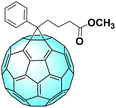
The most famous fullerene derivative used in solar cells is phenyl-C61-butyric acid methyl ester (PC61BM), whose structure can be seen in Fig. 3.41 This interesting C60 monoadduct was first synthesized and fully characterized in 1995 by the group of Prof. Fred Wudl. The group further analyzed this molecule and its interesting features, and at the end of the same year, PC61BM was first employed in a polymer solar cell.42 The authors found that a blend of the donor and acceptor results in an improvement of the carrier collection efficiency due to the large increase in the interfacial area and from the relatively short distance from any point in the donor polymer to a charge separation interface. PC61BM allows the creation of this network mostly thanks to the phenyl moiety, which has the tendency to undergo π–π stacking, either with other PC61BM molecules or with a suitable donor.Since this pioneering work, PC61BM has been employed in a whole lot of studies concerning OPVs.43,44 Recently, this molecule was used to obtain a deeper understanding of the mechanisms occurring in organic solar cells: the so-called “dark carriers” were found in the donor–acceptor blend, leading to an increase in the hole density and thus the recombination rate. In fact, the trapping and detrapping rates of the holes are tightly linked to the overall carrier lifetime.45 Resorting to PC61BM in these kinds of studies is indicative of the referential role assumed by PC61BM in the OPV field.
The encouraging results obtained with PC61BM paved the way for many different studies which dealt with small modifications in the reference structure, with the target of improving the performances of PC61BM. Step by step, all these small changes helped identify which modifications are the most favourable.
PC61BM leaves enough space for chemical modifications: the phenyl ring, the alkyl–ester chain, and last but not least the whole fullerene cage.46–71 The uncountable modifications undergone by PC61BM have not led to outstanding improvements most of the time. Thus, in this review we will enumerate just a few derivatives, those which for different reasons helped raising the quality of the solar cell.
Here the role of the solubility of the different materials cannot be underestimated. The solubility of the compounds is linked to the morphology of the resulting film, and thus to the performance of the solar device.46,47 For example, replacing phenyl with thiophene led to lower efficiencies due to poorer solubility.54 The relative solubility of the donor and acceptor is important as well; it should be similar in the analyzed solvent in order to achieve the best results.46
Concerning PC61BM derivatives, the best performances were obtained by replacing methyl with a cyanovinylene 4-nitrophenyl moiety, obtaining the derivative shown in Fig. 4A.59 The power conversion efficiency (PCE) of the cells containing this molecule as the acceptor reached 5.25% with the use of acetone/chloroform as a mixture of solvents to deposit the samples, which were then annealed. This led to a change in the crystallite size (as can be seen in the atomic force microscopy (AFM) images in Fig. 4B) and consequently of the electron and hole mobility.
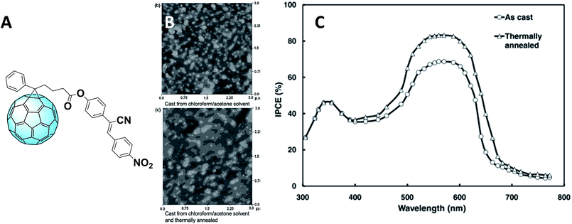 | ||
Fig. 4 (A) Structure of the fullerene derivative bearing a cyanovinylene 4-nitrophenyl moiety; (B) AFM images of the films without (above) and with annealing (below); (C) IPCE spectra of the devices based on the as-cast and thermally annealed P3HT![[thin space (1/6-em)]](https://www.rsc.org/images/entities/char_2009.gif) : :![[thin space (1/6-em)]](https://www.rsc.org/images/entities/char_2009.gif) F blend films deposited from mixed solvents. Reprinted from ref. 59 with permission of John Wiley and Sons.59 F blend films deposited from mixed solvents. Reprinted from ref. 59 with permission of John Wiley and Sons.59 | ||
Furthermore, the Incident Photon-to-electron Conversion Efficiency (IPCE) spectra (Fig. 4C) of the devices fabricated from mixed solvents showed a broader shape, leading to obtaining higher short-circuit current density (JSC) which can be ascribed as the cause of the higher PCE. Moreover, the IPCE of the devices containing this fullerene derivative is higher than that measured for PC61BM-containing devices. This might be due to the contribution of this novel derivative in the device absorption. In fact, the functionalizing moiety extends the absorption of the fullerene derivative to the visible region, hence improving that of the whole device. To further improve the morphology, covalent bonds were considered alongside the aforementioned π–π interactions. The introduction of reactive terminal groups with cross-linking abilities (Fig. 5A) increased morphological stability of the whole structure, conferring to the device higher long–term stability under operation.60Fig. 5B shows the transmission electron microscopy (TEM) images of a P3HT–PC61BM film (left) and a P3HT–PCBG film (right), both annealed at 140 °C for 1 hour. As it can be observed, the reactive epoxide terminal part allows the obtaining of a highly homogeneous film.
 | ||
| Fig. 5 (A) Structure of PCBG and (B) TEM images of the P3HT–PCBM film (left) and P3HT–PCBG film (right). Reprinted from ref. 60 with permission of The Royal Society of Chemistry. | ||
ICBA, the second in line
First synthesized by Neilands et al. in 1997 through a Diels–Alder reaction,72 the indene–C60 monoadduct was successfully incorporated into an organic solar cell several years later by Li and Hou et al.53 The good results obtained by the group with the monoadduct (3.89% PCE, very similar to 3.88% of PC61BM) were surpassed by those obtained with the bisadduct (IC60BA, Fig. 6).In fact, an outstanding PCE of 5.44% was obtained, thanks to the huge improvement of the open circuit voltage (VOC) from 0.58 V of PC61BM to 0.84 V. With respect to PC61BM, the presence of the two aryl groups improves both the solubility of IC60BA and its absorption in the visible range of the electromagnetic spectrum. These features both help the processability of the material for an easier incorporation into the solar cells and improve the performances of the devices. Furthermore, the LUMO of IC60BA is 0.17 eV higher than that of PC61BM (−3.91 eV). After optimization of the devices through thermal annealing, which smoothened the film surface, the same group could achieve an impressive PCE of 6.48%.73
Endohedral fullerenes
It is very common to run into the term “cage” while reading about fullerenes. In the present paper, this term has already been used several times. Interestingly, fullerenes can become full-fledged cages thanks to their peculiar ability to trap several species, such as atoms, ions, or small molecules.19,20 In general, these molecules are rather hard and expensive to produce. Nonetheless, their allure remains strong within the scientific community.One example of such a fullerene used in the field of OPV was reported by Drees et al.74 The group functionalized a lutetium-nitride containing C80 in order to tune the solubility and make this molecule suitable for the purpose. A schematic structure of Lu3N@C80–PCBH is depicted in Fig. 7. The reduced energy offset of the molecular orbitals of Lu3N@C80 compared to P3HT reduces energy losses in the charge transfer process and increases the VOC to 260 mV which is higher than those of PC61BM devices. OSCs prepared with Lu3N@C80–PCBH as an electron accepting material provided PCEs of up to 4.2%, while the best reference cell gave an efficiency of 3.4%.
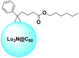 | ||
| Fig. 7 Schematic structure of Lu3N@C80–PCBH.74 | ||
Liedtke and Dyakonov et al. studied a similar derivative with a branched chain, discovering some limitations to its application.75 In fact, the weaker photoluminescence quenching which was registered for the endohedral containing devices results in less efficient charge carrier generation, and hence lower JSC. This might also be linked to an intramolecular electron exchange that competes with the donor-to-acceptor electron flow. Nonetheless, the significantly higher VOC (835 mV against 560 mV of the PC61BM containing cell) which was confirmed for the endohedral derivative once more highlights the potential of these structures.
Despite the attractions offered by endohedral fullerenes, the amount of research photovoltaic studies involving these outstanding materials is scarce. New kinds of photovoltaic technologies, such as PSCs, could bring these molecules again into consideration.
Fullerene dimers
Molecules containing more than one fullerene moiety have been the subject of several studies concerning OPV.76 Dyakonov and Martín et al. investigated several different homo- and heterodimers of C60 and C70.77 In the referenced study, the analysed heterodimers presented lower charge transfer ability than the homodimers, also shown by the reduced quenching of the photoluminescence lifetime of the polaron states formed during photoinduced absorption.Among the analyzed dimers, the C70-homodimer showed the best features for application in OPV, thanks to the longer separation induced by the phenyl moieties that form the bridge between the two fullerene cages, compromising the interaction between the acceptors and thus favouring the charge recombination processes.
A very promising outcome was obtained in 2013 by Murata et al., who could achieve an impressive result of 6.14% efficiency using a C60-homodimer.78 This value is highly comparable to 6.24% of PC61BM that the group obtained under the same conditions. A PC61BM dimer (Fig. 8A) which overcame its reference performance was proposed by Qin and Li et al.79 The better efficiency was attributed to a better morphology given by a different aggregation. This hypothesis was confirmed by AFM imaging, as can be seen in Fig. 8B.
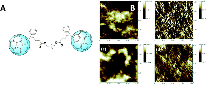 | ||
| Fig. 8 (A) Fullerene dimer as was synthesized by Qin and Li et al., and (B) AFM (4 4 mm) topography and phase images of the P3HT blend with either the simple derivative (a and b, above) or the dimer (c and d, below). Reprinted from ref. 79 with permission of The Royal Society of Chemistry. | ||
Fullerene dimers have also been used as additives in solar cells, to improve the morphology without affecting the photovoltaic performance.80 An optimal amount of fullerene dimer can also help enhancing the device lifetime.
Environmentally friendly fullerene-based solar cells
The main goal of research in photovoltaics is undoubtedly finding a renewable and eco-friendly source of energy. The urge to reduce the levels of pollution results in a “green approach” for the fabrication of organic devices. Burke and Lipomi suggested the use of green chemistry and environmentally friendly processing, as well as the replacement of fullerenes by other small molecules.81 The latter suggestion will be discussed in the following paragraphs. Nonetheless, there are a few examples of eco-friendlier fullerene-containing solar cells in the literature.82,83 For example, Bazan et al. synthesized a fullerene derivative soluble in 2-methyl-THF, a solvent obtained from agricultural by-products which is considerably less toxic than aromatic or halogenated solvents.84 This derivative was incorporated into solar cells with a PCE of ∼5%, paving the way to greener approaches to solar cell preparation.Furthermore, Oh, Kim, and Woo prepared a C60 bisadduct which, bearing hydrophilic chains, was soluble in a mixture of ethanol and water and thus allowed the preparation of solar cells through an eco-friendly process.85
Fullerene hole transporting materials
Fullerenes are well-known for their good electron-accepting ability; however they can behave also as electron donors when connected to suitable chemical moieties. For instance, Akasaka et al. demonstrated an efficient electron transfer from fullerene to tetracyano-9,10-anthra-p-quinodimethane on an endohedral metallofullerene-TCAQ conjugate.86 Concerning OPVs, the number of devices prepared with a fullerene derivative acting as a hole transporting material is scarce. Wang et al. performed studies of all-fullerene OPV devices, where the C70 acceptor is blended with either PC61BM or ICBA as supposed electron donors.87 The group wanted to take advantage of the difference in electron accepting ability existing between pristine C70 and the C60 derivatives, but the obtained PCEs were extremely low, mainly due to the insufficient hole transfer ability of the C60 derivatives, as claimed by the authors. As of today, there are still no successful studies where a fullerene derivative is used as a donor in OPV. Nonetheless, a suitable chemical functionalization of the fullerene sphere could address this issue in the next years. Such an approach will be later discussed, since this concept has already been demonstrated for PSCs.Beyond fullerenes
Nowadays, the interest of OPV researchers moved from fullerenes to non-fullerene small molecules.88–90 These non-fullerene acceptors allowed obtaining efficiencies exceeding 13%, together with improved stability.91,92 Nevertheless, the advent of PSCs has helped pristine and modified fullerenes to be again at the forefront of photovoltaic research. The impact of fullerenes over PSC rapid evolution will be discussed in the following section.Fullerenes for perovskite solar cells
PSCs: an introduction
Since the first papers about all-solid state hybrid PSCs were published, this new kind of technology has entered a virtuous cycle of improvement and rising interest.93,94At the beginning, these cells were considered a new type of dye-sensitized solar cell, but the working mechanism is supposed to be completely different from that of organic solar cells. In fact, when the perovskite gets irradiated, the formation of charges is almost immediate, and thus the working principle should be considered as non-excitonic.95
The main component of these cells is a hybrid organic–inorganic material, in which an organic cation, a metal, and a halide organize themselves into a specific crystal structure, typical of the perovskite. This material is able to harvest light and generate charges that are transferred either to a HTM or to an electron-transporting material (ETM), and consequently to the electrodes. Every single part of the PSC is currently under thorough investigation by the scientific community, in order to achieve the optimal working system.
The optimization of the charge transporting materials is one of the pathways that are being considered. A whole variety of new HTMs and some ETMs have been tried.96 The main role of the fullerenes in PSCs fits into this pathway: due to their aforementioned astonishing properties, fullerenes are the hotshot among organic molecules for replacing the most common electron-transporting material in PSCs, titanium dioxide.
TiO2 has been the material of choice for most of the investigations concerning PSCs with a regular configuration (Fig. 9A), but it is not immune to drawbacks, such as its degradation under UV irradiation.97
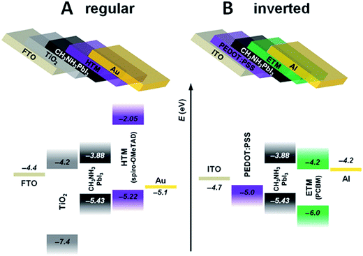 | ||
| Fig. 9 Most common planar perovskite configurations: (A) regular (FTO glass/ETM/PVSK/HTM/Au contact) and (B) inverted (ITO glass/HTM/PVSK/ETM/Al contact). Reprinted from ref. 96 with permission of John Wiley and Sons. | ||
Furthermore, the high temperature needed for the sintering process makes the layer-formation procedure rather complex and unsuitable for low-cost production and for the fabrication of flexible substrates.94
For these reasons, an alternative to TiO2 is highly desired for long-lasting, large-scale PSCs, and for the possibility to work with flexible cells.98
Fullerenes were first introduced into PSCs by Jeng et al.99 The planar PSC prepared by the group provided a PCE of 3.9%.
Together with the use of C60 and its derivatives as replacements for TiO2 in regular PSCs, great interest is also raised by the study of these molecules in inverted solar cells (Fig. 9B).100
In parallel to their use as ETMs, it is also important to consider the role of fullerenes as additives incorporated into the perovskite layer.101
Furthermore, very recently, a fullerene derivative suitably functionalized has also been reported to behave as an efficient hole transporting/electron blocking material in a PSC.102
Return of old acquaintances
In the light of what was found researching on OPV, PC61BM could not be exempted from thorough investigation relative to its application in PSCs. Just like in OPVs, in fact, PC61BM is nowadays the most famous organic ETM for PSCs.100 The HOMO and LUMO levels of PC61BM, which are −5.9 eV and −3.9 eV respectively, make it suitable for the purpose of extracting electrons and block holes coming from methylammonium lead iodide, whose valence and conduction bands are −5.4 eV and −3.9 eV, respectively.103 For these reasons, PC61BM has been often used in inverted PSCs to achieve remarkable power conversion efficiencies.104,105One of the major challenges regarding fullerene materials is to reach equilibrium between the film morphology and the electron transporting ability. For this, the PC61BM layer should be thin enough to ensure an efficient electron transport, together with suppressed charge recombination and low series resistance.
To achieve these properties, a rather continuous film is required. However, the thin PC61BM films may not be able to completely cover the perovskite film due to the small molecule nature of PC61BM and the low viscosity of the PC61BM solution.106
Several groups have tried to bypass this problem. Zhao, Yang, and Yan et al., for example, doped the PC61BM layer with polystyrene in order to get a smoother and more continuous film.107 Several other molecules have been used to dope or modify PC61BM with success.108–112 In particular, doping the PC61BM layer with graphene oxide improved the conductivity, and reduced the series resistance and surface roughness, as shown in Fig. 10.113
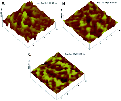 | ||
| Fig. 10 AFM images of the (A) perovskite, (B) perovskite with an upper PC61BM layer, and (C) perovskite with graphene oxide:PC61BM as an electron transporting layer. Reprinted from ref. 113 with permission of John Wiley and Sons. | ||
Doping is not the only route to achieve better performance from the use of PC61BM. Huang et al., for example, highlighted the importance of decreasing the energy disorder in electron transporting layers (ETLs) in order to improve the VOC in PSCs, without affecting JSC and the fill factor (FF). Through the use of a solvent annealing process, the PCE is increased from 17.1 to 19.4% by the group.114
Other strategies involving the use of PC61BM do not leave out TiO2. More than once, the inorganic ETL has been functionalized with self-assembling fullerene monolayers, in order to generate a well-ordered structure, and, therefore, to improve the reproducibility of the performance. In general, owing to the appropriate LUMO level, the electrons might pass from the perovskite layer to the fullerene and vice versa, so that the monolayer acts as an electron “deposit”. This leads to a reduction in the loss of VOC and, therefore, to an improved performance of the whole device.115,116
Just like in OPVs, several PC61BM derivatives have also been tried. For example, PC71BM was used several times as an ETM in PSCs, giving remarkable results. In particular, Wu et al. highlighted the importance of the solvent in which the fullerene molecule is processed, since it can influence the interface between the layer and the perovskite.117 By optimizing the preparation of their inverted devices, the group could achieve an impressive PCE of 18%.118
Together with PC61BM analogues, the aforementioned indene derivatives have also been tried, given the good results they provided in OPV. However, both IC60BA and IC60TA presented higher hysteresis than the C60 reference and PC61BM.119
The latter is not the only example in which performances given by several fullerenes were compared with each other within the same study.120 Jen et al. studied the different behaviour of PC61BM, C60 and IC60BA, highlighting the correlation between the electron mobility of the different fullerenes and the performance of the devices into which they are incorporated.121 The results of this study indicated that high-mobility fullerenes can effectively allow the charge transport, and that C60 would be a better electron transporter than PC61BM, but its use is limited by its scarce processability.
The uses of PC61BM are not limited to its application as an ETM. The addition of fullerenes directly into the perovskite may also produce relevant beneficial effects. Sargent et al. prepared perovskite layers in which the distribution of PC61BM was controlled by dissolving it previously in chlorobenzene and subsequently mixing it with the perovskite solution before deposition.122 According to the authors, the presence of PC61BM close to perovskite grain boundaries has a significant impact on electronic properties and hence on the hysteresis, as it will be explained further.
Another interesting way to employ fullerenes as additives is presented by Dennis, Wang, Bi, and Grätzel et al., who used PC61BM and α-bis-PCBM (equatorial bisadduct).123 Both fullerenes were dissolved in the so-called “antisolvent”, a solvent that cannot attack the perovskite, like chlorobenzene. The antisolvent is dripped on the perovskite during the spin-coating deposition in order to improve the crystallization thanks to repulsive forces.124 The group reported that α-bis-PCBM creates a hydrophobic network which resists moisture incursion, thus preventing the erosion of the perovskite, and passivating the voids or pinholes generated. α-bis-PCBM also presented improved electron extraction efficiency, and allowed better crystallization of the perovskite. The considerably better films obtained through this technique are shown in Fig. 11.
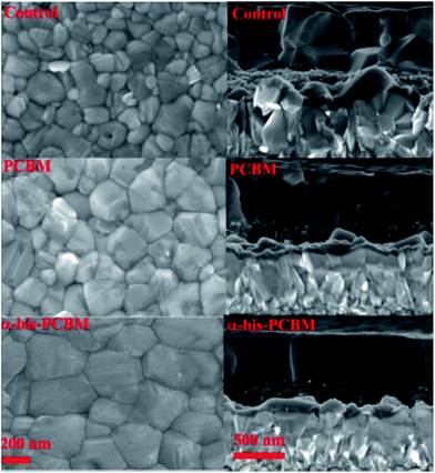 | ||
| Fig. 11 SEM images: top view (left) and cross section (right) of the, from top to bottom, perovskite reference, perovskite treated with PC61BM-containing antisolvent, and perovskite treated with α-bis-PCBM-containing antisolvent. Reprinted from ref. 123 with permission of John Wiley and Sons. | ||
Hysteresis and fullerenes
Hysteresis causes a discrepancy between the cell performances when they are measured either backwards (from a definite voltage value to 0) or forwards (from zero to a definite voltage value) and results in an inaccurate efficiency measurement when this is extracted from a current density–voltage (J–V) curve.125–128 Thus, this phenomenon should be avoided when we consider the future commercialization and upscaling of PSCs.Hysteresis seems to be the consequence of three major effects: interfacial charge accumulation, charge traps, and ion migration. Several studies have led to the conclusion that fullerenes can actually limit, if not completely remove, each one of these possible causes.25 In the paper that can be considered the precursor of the study linking fullerenes and hysteresis suppression in PSCs, Sargent et al. found out that PC61BM was able to bond with Pb–I antisite defects, thus suppressing trap states which occur on the surface of grain boundaries.129 These are also the preferred channels for ion migration, thought to be another cause of hysteresis. In the same work, it is shown how fullerenes are able to fill these boundaries, hence blocking these channels.
Another curious finding involving PC61BM in hysteresis is the one reported by Bryant and Durrant et al. Their “hysteresis-free” inverted solar cell with PC61BM as an ETL showed some hysteretic behaviour when cooled down to lower temperatures (Fig. 12).130 Curiously, while from 293 K to 175 K hysteresis notably increases, it looks like it decreases again at 77 K.
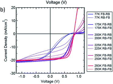 | ||
| Fig. 12 JV curves obtained under simulated 1 sun illumination for a fullerene top cathode MAPbI3 cell backwards (RB, solid line) and forwards (FB, dashed line) at temperatures ranging between 77 and 293 K at scan speeds of 0.125 V s−1. Reprinted from ref. 129 with permission of the American Chemical Society. | ||
To try to explain this phenomenon, we should first talk about some fundamental processes occurring in semiconductors while operating. After being subjected to an electric field, the generated change in dielectric polarization is rapidly combated by the tendency to the equilibrium. The phenomenon that occurs while reaching a new equilibrium is called relaxation, and the time taken to reach equilibrium is named the relaxation time. Apparently, the relaxation time of JSC increases as the temperature decreases, and so the loss in photocurrent increases as temperature decreases. The relaxation time has shown to be linked with capacitance, since both depend on several device and experiment parameters, such as temperature, perovskite thickness, and device architecture. Slow charging and discharging processes favour hysteresis.131 This is consistent with the data registered for temperatures from 293 K to 175 K. At 77 K, the relaxation time is higher than the employed scan speed, so the hysteresis-causing processes are slowed down to a lower speed than that needed to detect the hysteresis.
Polyethylene glycol and fullerenes
When thinking of a possible structure with the ability to protect the perovskite against moisture, the first characteristic that we expect is hydrophobicity. In order to repel water molecules, a structure that has no affinity with these should be the logical selection. For example, in the work of Huang et al., a –CF3 containing molecule is used to dope the fullerene in order to increase its hydrophobicity, giving good results in terms of stability and efficiency.132Nonetheless, polyethylene glycol (PEG), which is not hydrophobic, showed an unexpected protective effect against moisture when introduced into the perovskite layer.
Starting from the analysis of the cause of the reversible degradation of the perovskite in water as explained by Walsh et al.,133 Zhao, Wei, and Li et al. tried to override it by introducing a molecule that captured water instead of repelling it.134 That is where PEG comes in: potentially binding water molecules; it is speculated that it prevents water molecules from approaching the perovskite by coordinating them. Eventually, the authors demonstrated the feasibility of this strategy, obtaining highly resistant perovskite layers which withstand ambient moisture.
Similarly, also the group of Zhao et al. introduced PC61BM into the perovskite, and helped by the positive effect of polyethylene glycol (PEG) obtained devices with significantly reduced hysteresis and improved stability.135
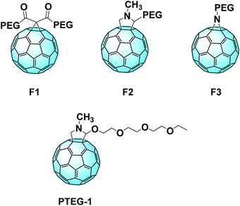
A comparable approach involving a covalent linkage between PEG and fullerene was proposed by Grätzel and Delgado et al. The group synthesized three novel C60 derivatives, each one linked to PEG chains through different bridges (Fig. 13, top).101 A small amount of these fullerene derivatives significantly enhances the device stability against the moisture. MAPbI3:PEG-[60]fullerene devices containing F1, F2, and F3 maintain up to 97% of their initial PCE after 300 hours.
Recently, Loi et al. reported a novel C60 derivative (PTEG-1, Fig. 13, bottom) which overtook the performances of their PC61BM reference: the performance increased from 11.8% to 13.1% with the use of the new derivative, which reached 16.1% after optimization.136 Furthermore, the group investigated how the so called light-soaking effect is correlated with the dielectric constant of the material. This effect can be noticed when, after exposure to light, the efficiency of the device increases significantly. The higher dielectric constant of the novel derivative seems to be linked to a reduction of the surface trap state concentration, and so the light-soaking effect is considerably lower. This seems to be linked to the high dielectric constant of the novel fullerene (5.9 with respect to 3.9 of PC61BM). The higher-constant derivative helps screening the recombination between the traps and the free electrons in the extraction layer. Furthermore, it seems that also the side chain contributes to the passivation of the electron traps.137
Fullerenes as hole transporting/electron blocking layers in PSCs
In summary, we reported for the first time a HTM based on fullerenes. An appropriate chemical design has allowed tailoring the HOMO and LUMO levels of FU7, making it able to block electrons and act as a hole selective contact. This molecule has been applied as the HTM in PSCs without any additive. Significant efficiencies have been reported obtaining 0.77 on average (0.81 for champion devices) times the performance of the reference cell prepared with doped spiro-OMeTAD. In addition, cells prepared with FU7 present higher stability than the reference cells. The presence of fullerenes plays a structural key role in the HTM as it permits the formation of spherical molecules with charge separation, an easy transport pathway interconnection and an increase in the structural order of the film resulting in higher device performance. Finally, we have reported for the first time efficient “fullerene sandwich” PSCs where both selective contacts are fullerene-based systems and the active layer itself also contains fullerenes. Our results could have important implications in the development of a new branch in the family of fullerene derivatives, taking advantage of the enormous knowledge already acquired in the synthesis of these kinds of compounds but applying in a completely new field as HTLs and electron blocking systems.Even though fullerenes are well known thanks to their outstanding ability to accept and transport electrons, a suitable chemical modification carried out on the fullerene sphere has recently questioned this dogma.102 The hexafunctionalization of fullerenes with hole transporting fragments allows a fine tuning of energy levels, yielding a fullerene material which is able to block electrons and transport holes. The presence of fullerenes plays a key role in the structure as it leads to the formation of spherical molecules with a clear charge separation and an easy transport pathway interconnection. The nice globular structure of this novel molecule, named FU7, is shown in Fig. 14.
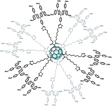 | ||
| Fig. 14 Structure of the novel derivative FU7.102 | ||
Without using additives, significant efficiencies have been obtained, reaching 0.81 times the performance of the reference cell prepared with regularly doped spiro-OMeTAD.
Proven the ability of this molecule to act as a HTM, a fullerene sandwich solar cell containing fullerene-based materials in both the ETL and HTL and also in the perovskite active layer as an additive was fabricated (Fig. 15). Without any optimization, a promising efficiency of 9% was obtained for the first time for a “fullerene sandwich” perovskite device. This work opens a wide range of design possibilities for organic compounds and devices in the future, both in the field of organic and hybrid photovoltaics.
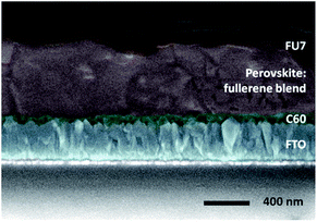 | ||
| Fig. 15 Cross-section Field Emission Scanning Electron Microscopy (FE-SEM) micrograph of a “fullerene sandwich” perovskite device with architecture FTO/C60/pvsk:C60/FU7/Au. The local thickness of the fullerene layers depends on the roughness of the layer on which they are deposited, being 10–40 nm for C60 and 10–50 nm for FU7. Reprinted from ref. 102 with permission of John Wiley and Sons. | ||
Novel fullerenes for perovskite solar cells
As it happened with OPV, once it was demonstrated that pristine fullerene and PC61BM could play an important role in PSCs, several new derivatives were prepared and incorporated into devices.A nice alternative to PC61BM was presented by Echegoyen et al., who prepared a C60-fulleropyrrolidine (DMEC60) and its C70 analogue (DMEC70), whose structures are shown in Fig. 16.138 Both were used in inverted PVSK devices and compared to the corresponding PCBM, overcoming their performances in each case: DMEC60 and DMEC70 yielded PCEs of 15.2% and 16.4% respectively, while the corresponding PCBMs yielded no more than 14.5% (PC61BM) and 15.1% (PC71BM). These astonishing results are attributed to several factors, such as more suitable energy levels, better electron mobility and charge extraction ability with respect to the PCBMs, the latter being attributed to favourable interactions between the perovskite structure and the functionalizing moieties. Moreover, the stability of the devices was improved using these two derivatives. This was explained by analyzing the wetting capability of the surfaces: apparently, the pyrrolidine moieties make the molecule more hydrophobic, and thus prone to rejecting water. Another explanation could be linked to the favourable interactions between the novel derivatives and the perovskite, which make the layers strong enough to delay the migration of the metal contact into the light-harvesting layer. Last but not least, the synthesis of these derivatives is easier and with higher yields than PC61BM, hence offering a valid alternative to the latter.
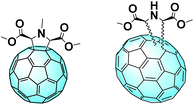 | ||
| Fig. 16 Structure of DMEC60 and model of the DMEC70 isomers.138 | ||
These findings were confirmed by Xu and Han et al., who prepared a bisadduct of DMEC60 (bis-DMEC60) and tested it in printable mesoscopic PSCs. The better results obtained using the bisadduct with respect to those obtained with the monoadduct once again suggest that the interactions between the perovskite and the functionalizing pyrrolidine moieties play a fundamental role.139
Echegoyen et al. also prepared a PC61BM dimer and used it as the ETM in planar inverted PSCs.140 The efficiency of the cells prepared recurring to this fullerene derivative (16.6%) overcame that of these including PC61BM (14.7%). The higher hydrophobicity of the novel dimer enhances the stability of the device by protecting the perovskite against moisture.
A series of two isoxazolinofullerenes and two pyrazolinofullerenes was prepared by Tena-Zaera, Martín, and Delgado et al.141 Analyzing the four novel fullerenes, a correlation between the obtained VOC and the LUMO of the fullerene material was found, the thing that is indeed useful for the design of new molecules. The results obtained with these molecules outrun in every case those obtained with the reference. The peculiarity of this work is that the fullerenes are employed in ETL-free devices through the “fullerene saturation approach”.142 This strategy consists in preparing the fullerene solution by dissolving the components in a solvent which was previously saturated with the required fullerene. The fullerene-saturated perovskite allowed the preparation of ETL-free devices with improved performances with respect to ref. 143 In fact, the fullerene-containing cell presented a significantly decreased recombination rate, probably due to the well-known passivating effect of the fullerene cage, which lowers the opportunities of recombination.144
Together with ETL-free devices the “fullerene saturation approach” allowed the preparation of efficient TiO2-free cells, using C60 or C70 as ETLs.142 Another example of TiO2-free PSCs is given by Lamberti and Petrozza et al., who reported a fullerene-modified FTO fabricated stable and efficient PSC. These devices provide the great advantage of simplifying upscaling, thanks to the low-temperature processing.145
Conclusions
In this review we reported those we think to be amongst the most important and peculiar findings concerning fullerenes in photovoltaics. In summary, fullerenes have been extensively used in OPV, thanks to their unique features, such as the ability to accept electrons, the ease to functionalize the surface with a wide range of different reactions, and the possibility of incorporating small structures inside the cage. Employing fullerenes in these kinds of solar cells allowed finding the parameters that most influence the performance of the OPV devices, one among many the solubility, which has to be similar between the fullerene and the donor. Passing from OPVs to PSCs, another important role of fullerenes was found, namely the ability to passivate trap states that are generated at the interface with the perovskite, therefore reducing hysteresis. Nowadays, further functionalization of the fullerene cage aims to address the issue of stability, employing fullerenes as additives put directly into perovskites.The amazing features of this family of molecules never cease to surprise us, so it is rather important to keep on investigating its applications in photovoltaics, in order to achieve good performing and stable cells that could finally break through the silicon-dominated market.
Conflicts of interest
The authors state that there are no conflicts of interest to declare concerning this paper.Acknowledgements
S. C. acknowledges the Basque Government for a PREDOC grant. J. L. D. acknowledges Ikerbasque, the Basque Foundation for Science, for an “Ikerbasque Research Fellow” contract, the Polymat Foundation and MINECO of Spain for IEDI–2015–00666 and CTQ2015–70921 grants, and the Iberdrola Foundation for financial support.References
- H. Aldersey-Williams, The Most Beautiful Molecule-The Discovery of the Buckyball, John Wiley & Sons, Inc., 1995 Search PubMed.
- The Nobel Prize in Chemistry, https://www.nobelprize.org/nobel_prizes/chemistry/laureates/1996/.
- D. E. H. Jones, New Sci., 1966, 245 Search PubMed.
- D. E. H. Jones, The Inventions of Daedalus, Freeman, Oxford, 1982 Search PubMed.
- E. Osawa, Superaromaticity, Kagaku, 1970, vol. 25, pp. 854–863 Search PubMed.
- D. Bochvar and E. Galpern, Dokl. Akad. Nauk SSSR, 1973, 209, 610–612 Search PubMed.
- R. A. Davidson, Theor. Chim. Acta, 1981, 58, 193–231 CrossRef.
- H. W. Kroto, Angew. Chem., Int. Ed., 1992, 31, 111–129 CrossRef.
- R. E. Smalley, Science, 1991, 31, 22–28 Search PubMed.
- H. W. Kroto, J. R. Heath, S. C. O'Brien, R. F. Curl and R. E. Smalley, Nature, 1985, 318, 162 CrossRef.
- Buckyball Molecule, https://statesymbolsusa.org/symbol-official-item/texas/state-award-recognition/buckyball-molecule.
- P. R. Buseck, S. J. Tsipursky and R. Hettich, Science, 1992, 257, 215–217 CrossRef PubMed.
- H. W. Kroto, Nature, 1987, 329, 529 CrossRef.
- R. C. Haddon, R. E. Palmer, H. W. Kroto and P. A. Sermon, Philos. Trans. R. Soc. London, Ser. A, 1993, 343, 53–62 CrossRef.
- S. Kirner, M. Sekita and D. M. Guldi, Adv. Mater., 2014, 26, 1482–1493 CrossRef PubMed.
- C. A. Reed and R. D. Bolskar, Chem. Rev., 2000, 100, 1075–1120 CrossRef PubMed.
- E. Frankevich, Y. Maruyama and H. Ogata, Chem. Phys. Lett., 1993, 214, 39–44 CrossRef.
- O. A. Gudaev, V. K. Malinovsky, A. V. Okotrub and Y. V. Shevtsov, Fullerene Sci. Technol., 1998, 6, 433–443 CrossRef.
- A. A. Popov, S. Yang and L. Dunsch, Chem. Rev., 2013, 113, 5989–6113 CrossRef PubMed.
- S. Yang, T. Wei and F. Jin, Chem. Soc. Rev., 2017, 46, 5005–5058 RSC.
- M. Prato, J. Mater. Chem., 1997, 7, 1097–1109 RSC.
- A. Hirsch, The Chemistry of the Fullerenes, Wiley VCH, 2008 Search PubMed.
- A. Hirsch, M. Brettreich and F. Wudl, Fullerenes Chemistry and Reactions, Wiley VCH, 2004 Search PubMed.
- E. Castro, A. H. Garcia, G. Zavala and L. Echegoyen, J. Mater. Chem. B, 2017, 5, 6523–6535 RSC.
- Y. Fang, C. Bi, D. Wang and J. Huang, ACS Energy Lett., 2017, 2, 782–794 CrossRef.
- M. S. Fuhrer, J. Nygård, L. Shih, M. Forero, Y.-G. Yoon, M. S. C. Mazzoni, H. J. Choi, J. Ihm, S. G. Louie, A. Zettl and P. L. McEuen, Science, 2000, 288, 494–497 CrossRef PubMed.
- I. Jeon, Y. Matsuo and S. Maruyama, Top. Curr. Chem., 2018, 376, 4 CrossRef PubMed.
- H. Imahori and Y. Sakata, Adv. Mater., 1997, 9, 537–546 CrossRef.
- S. Collavini and J. L. Delgado, Adv. Energy Mater., 2017, 7, 1601000 CrossRef.
- (a) J. L. Delgado, P. A. Bouit, S. Filippone, M. A. Herranz and N. Martin, Chem. Commun., 2010, 46, 4853–4865 RSC; (b) J. L. Delgado, M. A. Herranz and N. Martín, J. Mater. Chem., 2008, 18, 1417–1426 RSC; (c) J. L. Delgado, N. Martín, P. de la Cruz and F. Langa, Chem. Soc. Rev., 2011, 40, 5232–5241 RSC.
- F. Zhang, O. Inganäs, Y. Zhou and K. Vandewal, Natl. Sci. Rev., 2016, 3, 222–239 CrossRef.
- L.-L. Deng, S.-Y. Xie and F. Gao, Adv. Electron. Mater., 2017, 1700435 CrossRef.
- E. Castro, J. Murillo, O. Fernandez-Delgado and L. Echegoyen, J. Mater. Chem. C, 2018, 6, 2635–2651 RSC.
- R. Ganesamoorthy, G. Sathiyan and P. Sakthivel, Sol. Energy Mater. Sol. Cells, 2017, 161, 102–148 CrossRef.
- L. L. Deng, S. Y. Xie and F. Gao, Adv. Electron. Mater., 2017, 0, 1700435 CrossRef.
- T. Gatti, E. Menna, M. Meneghetti, M. Maggini, A. Petrozza and F. Lamberti, Nano Energy, 2017, 41, 84–100 CrossRef.
- S. Rafique, S. M. Abdullah, K. Sulaiman and M. Iwamoto, Renewable Sustainable Energy Rev., 2018, 84, 43–53 CrossRef.
- N. Marinova, S. Valero and J. L. Delgado, J. Colloid Interface Sci., 2017, 488, 373–389 CrossRef PubMed.
- F. Matsumoto, T. Iwai, K. Moriwaki, Y. Takao, T. Ito, T. Mizuno and T. Ohno, ACS Appl. Mater. Interfaces, 2016, 8, 4803–4810 CrossRef PubMed.
- C.-L. Chang, C.-W. Liang, J.-J. Syu, L. Wang and M.-k. Leung, Sol. Energy Mater. Sol. Cells, 2011, 95, 2371–2379 CrossRef.
- J. C. Hummelen, B. W. Knight, F. LePeq and F. Wudl, J. Org. Chem., 1995, 60, 532–538 CrossRef.
- G. Yu, J. Gao, J. C. Hummelen, F. Wudl and A. J. Heeger, Science, 1995, 270, 1789–1791 CrossRef.
- S. E. Shaheen, C. J. Brabec, N. S. Sariciftci, F. Padinger, T. Fromherz and J. C. Hummelen, Appl. Phys. Lett., 2001, 78, 841–843 CrossRef.
- G. Li, V. Shrotriya, J. Huang, Y. Yao, T. Moriarty, K. Emery and Y. Yang, Nat. Mater., 2005, 4, 864–868 CrossRef.
- S. D. Oosterhout, A. J. Ferguson, B. W. Larson, D. C. Olson and N. Kopidakis, J. Phys. Chem. C, 2016, 120, 24597–24604 CrossRef.
- P. A. Troshin, H. Hoppe, J. Renz, M. Egginger, J. Y. Mayorova, A. E. Goryachev, A. S. Peregudov, R. N. Lyubovskaya, G. Gobsch, N. S. Sariciftci and V. F. Razumov, Adv. Funct. Mater., 2009, 19, 779–788 CrossRef.
- C. Yang, J. Y. Kim, S. Cho, J. K. Lee, A. J. Heeger and F. Wudl, J. Am. Chem. Soc., 2008, 130, 6444–6450 CrossRef PubMed.
- F. B. Kooistra, J. Knol, F. Kastenberg, L. M. Popescu, W. J. H. Verhees, J. M. Kroon and J. C. Hummelen, Org. Lett., 2007, 9, 551–554 CrossRef PubMed.
- H. U. Kim, J.-H. Kim, H. Kang, A. C. Grimsdale, B. J. Kim, S. C. Yoon and D.-H. Hwang, ACS Appl. Mater. Interfaces, 2014, 6, 20776–20785 CrossRef PubMed.
- Y. Zhang, H.-L. Yip, O. Acton, S. K. Hau, F. Huang and A. K. Y. Jen, Chem. Mater., 2009, 21, 2598–2600 CrossRef.
- S.-O. Kim, D. Sung Chung, H. Cha, J. Wan Jang, Y.-H. Kim, J.-W. Kang, Y.-S. Jeong, C. E. Park and S.-K. Kwon, Sol. Energy Mater. Sol. Cells, 2011, 95, 432–439 CrossRef.
- L. M. Popescu, P. van 't Hof, A. B. Sieval, H. T. Jonkman and J. C. Hummelen, Appl. Phys. Lett., 2006, 89, 213507 CrossRef.
- Z. Tan, S. Li, F. Wang, D. Qian, J. Lin, J. Hou and Y. Li, Sci. Rep., 2014, 4, 4691 CrossRef PubMed.
- S.-C. Chuang, C.-W. Chiu, S.-C. Chien, C.-W. Chu and F.-C. Chen, Synth. Met., 2011, 161, 1264–1269 CrossRef.
- L. Zheng, Q. Zhou, X. Deng, M. Yuan, G. Yu and Y. Cao, J. Phys. Chem. B, 2004, 108, 11921–11926 CrossRef.
- Y. Yu, B. Jin, R. Peng, L. Fan, L. Cai, B. Fan and S. Chu, Synth. Met., 2016, 212, 44–50 CrossRef.
- C. Liu, S. Xiao, X. Shu, Y. Li, L. Xu, T. Liu, Y. Yu, L. Zhang, H. Liu and Y. Li, ACS Appl. Mater. Interfaces, 2012, 4, 1065–1071 CrossRef PubMed.
- M. Lv, M. Lei, J. Zhu, T. Hirai and X. Chen, ACS Appl. Mater. Interfaces, 2014, 6, 5844–5851 CrossRef PubMed.
- J. A. Mikroyannidis, A. N. Kabanakis, S. S. Sharma and G. D. Sharma, Adv. Funct. Mater., 2011, 21, 746–755 CrossRef.
- M. Drees, H. Hoppe, C. Winder, H. Neugebauer, N. S. Sariciftci, W. Schwinger, F. Schaffler, C. Topf, M. C. Scharber, Z. Zhu and R. Gaudiana, J. Mater. Chem., 2005, 15, 5158–5163 RSC.
- G. Zhao, Y. He, Z. Xu, J. Hou, M. Zhang, J. Min, H.-Y. Chen, M. Ye, Z. Hong, Y. Yang and Y. Li, Adv. Funct. Mater., 2010, 20, 1480–1487 CrossRef.
- M. M. Wienk, J. M. Kroon, W. J. H. Verhees, J. Knol, J. C. Hummelen, P. A. van Hal and R. A. J. Janssen, Angew. Chem., Int. Ed., 2003, 42, 3371–3375 CrossRef PubMed.
- S. H. Park, A. Roy, S. Beaupre, S. Cho, N. Coates, J. S. Moon, D. Moses, M. Leclerc, K. Lee and A. J. Heeger, Nat. Photonics, 2009, 3, 297–302 CrossRef.
- W. S. Shin, J.-C. Lee, J.-R. Kim, H. Y. Lee, S. K. Lee, S. C. Yoon and S.-J. Moon, J. Mater. Chem., 2011, 21, 960–967 RSC.
- S. P. Singh, C. H. P. Kumar, G. D. Sharma, R. Kurchania and M. S. Roy, Adv. Funct. Mater., 2012, 22, 4087–4095 CrossRef.
- F. B. Kooistra, V. D. Mihailetchi, L. M. Popescu, D. Kronholm, P. W. M. Blom and J. C. Hummelen, Chem. Mater., 2006, 18, 3068–3073 CrossRef.
- M. Lenes, G.-J. A. H. Wetzelaer, F. B. Kooistra, S. C. Veenstra, J. C. Hummelen and P. W. M. Blom, Adv. Mater., 2008, 20, 2116–2119 CrossRef.
- M. Lenes, S. W. Shelton, A. B. Sieval, D. F. Kronholm, J. C. Hummelen and P. W. M. Blom, Adv. Funct. Mater., 2009, 19, 3002–3007 CrossRef.
- L. Ye, S. Zhang, D. Qian, Q. Wang and J. Hou, J. Phys. Chem. C, 2013, 117, 25360–25366 CrossRef.
- Y. Lin, J. A. Lim, Q. Wei, S. C. B. Mannsfeld, A. L. Briseno and J. J. Watkins, Chem. Mater., 2012, 24, 622–632 CrossRef.
- D. K. Susarova, A. E. Goryachev, D. V. Novikov, N. N. Dremova, S. M. Peregudova, V. F. Razumov and P. A. Troshin, Sol. Energy Mater. Sol. Cells, 2014, 120, 30–36 CrossRef.
- A. Puplovskis, J. Kacens and O. Neilands, Tetrahedron Lett., 1997, 38, 285–288 CrossRef.
- G. Zhao, Y. He and Y. Li, Adv. Mater., 2010, 22, 4355–4358 CrossRef PubMed.
- R. B. Ross, C. M. Cardona, D. M. Guldi, S. G. Sankaranarayanan, M. O. Reese, N. Kopidakis, J. Peet, B. Walker, G. C. Bazan, E. Van Keuren, B. C. Holloway and M. Drees, Nat. Mater., 2009, 8, 208 CrossRef PubMed.
- M. Liedtke, A. Sperlich, H. Kraus, A. Baumann, C. Deibel, M. J. M. Wirix, J. Loos, C. M. Cardona and V. Dyakonov, J. Am. Chem. Soc., 2011, 133, 9088–9094 CrossRef PubMed.
- S. Erten-Ela, C. Villegas, J. L. Delgado and N. Martin, New J. Chem., 2015, 39, 1477–1482 RSC.
- (a) J. L. Delgado, E. Espíldora, M. Liedtke, A. Sperlich, D. Rauh, A. Baumann, C. Deibel, V. Dyakonov and N. Martín, Chem.–Eur. J., 2009, 15, 13474–13482 CrossRef PubMed; (b) O. G. Poluektov, J. Niklas, K. L. Mardis, S. Beaupré, M. Leclerc, C. Villegas, S. E. Ela, J. L. Delgado, N. Martín, A. Sperlich and V. Dyakonov, Adv. Energy Mater., 2014, 4, 1301517 CrossRef; (c) E. Espíldora, J. L. Delgado and N. Martín, Isr. J. Chem., 2014, 54, 429–439 CrossRef.
- Y. Morinaka, M. Nobori, M. Murata, A. Wakamiya, T. Sagawa, S. Yoshikawa and Y. Murata, Chem. Commun., 2013, 49, 3670–3672 RSC.
- J. Liu, X. Guo, Y. Qin, S. Liang, Z.-X. Guo and Y. Li, J. Mater. Chem., 2012, 22, 1758–1761 RSC.
- B. C. Schroeder, Z. Li, M. A. Brady, G. C. Faria, R. S. Ashraf, C. J. Takacs, J. S. Cowart, D. T. Duong, K. H. Chiu, C.-H. Tan, J. T. Cabral, A. Salleo, M. L. Chabinyc, J. R. Durrant and I. McCulloch, Angew. Chem., Int. Ed., 2014, 53, 12870–12875 CrossRef PubMed.
- D. J. Burke and D. J. Lipomi, Energy Environ. Sci., 2013, 6, 2053–2066 RSC.
- S. Zhang, L. Ye, H. Zhang and J. Hou, Mater. Today, 2016, 19, 533–543 CrossRef.
- Y. Chen, Y. Cui, S. Zhang and J. Hou, Polym. Chem., 2015, 6, 4089–4095 RSC.
- X. Chen, X. Liu, M. A. Burgers, Y. Huang and G. C. Bazan, Angew. Chem., Int. Ed., 2014, 53, 14378–14381 CrossRef PubMed.
- T. L. Nguyen, C. Lee, H. Kim, Y. Kim, W. Lee, J. H. Oh, B. J. Kim and H. Y. Woo, Macromolecules, 2017, 50, 4415–4424 CrossRef.
- Y. Takano, S. Obuchi, N. Mizorogi, R. García, M. Á. Herranz, M. Rudolf, D. M. Guldi, N. Martín, S. Nagase and T. Akasaka, J. Am. Chem. Soc., 2012, 134, 19401–19408 CrossRef PubMed.
- T. Zhuang, X.-F. Wang, T. Sano, Z. Hong, Y. Yang and J. Kido, Appl. Phys. Lett., 2013, 103, 203301 CrossRef.
- C. Yan, S. Barlow, Z. Wang, H. Yan, A. K. Y. Jen, S. R. Marder and X. Zhan, Nat. Rev. Mater., 2018, 3, 18003 CrossRef.
- N. Liang, W. Jiang, J. Hou and Z. Wang, Mater. Chem. Front., 2017, 1, 1291–1303 RSC.
- W. Chen and Q. Zhang, J. Mater. Chem. C, 2017, 5, 1275–1302 RSC.
- W. Zhao, S. Li, H. Yao, S. Zhang, Y. Zhang, B. Yang and J. Hou, J. Am. Chem. Soc., 2017, 139, 7148–7151 CrossRef PubMed.
- Y. Cui, H. Yao, B. Gao, Y. Qin, S. Zhang, B. Yang, C. He, B. Xu and J. Hou, J. Am. Chem. Soc., 2017, 139, 7302–7309 CrossRef PubMed.
- H.-S. Kim, C.-R. Lee, J.-H. Im, K.-B. Lee, T. Moehl, A. Marchioro, S.-J. Moon, R. Humphry-Baker, J.-H. Yum, J. E. Moser, M. Grätzel and N.-G. Park, Sci. Rep., 2012, 2, 591 CrossRef PubMed.
- M. M. Lee, J. Teuscher, T. Miyasaka, T. N. Murakami and H. J. Snaith, Science, 2012, 338, 643 CrossRef PubMed.
- (a) S. Collavini, S. F. Völker and J. L. Delgado, Angew. Chem., Int. Ed., 2015, 54, 9757–9759 CrossRef PubMed; (b) S. Collavini, S. F. Völker and J. L. Delgado, Angew. Chem., 2015, 127, 9893–9895 CrossRef.
- S. F. Völker, S. Collavini and J. L. Delgado, ChemSusChem, 2015, 8, 3012–3028 CrossRef PubMed.
- T. Leijtens, G. E. Eperon, S. Pathak, A. Abate, M. M. Lee and H. J. Snaith, Nat. Commun., 2013, 4, 2885 CrossRef PubMed.
- J. You, Z. Hong, Y. Yang, Q. Chen, M. Cai, T.-B. Song, C.-C. Chen, S. Lu, Y. Liu, H. Zhou and Y. Yang, ACS Nano, 2014, 8, 1674–1680 CrossRef PubMed.
- J.-Y. Jeng, Y.-F. Chiang, M.-H. Lee, S.-R. Peng, T.-F. Guo, P. Chen and T.-C. Wen, Adv. Mater., 2013, 25, 3727–3732 CrossRef PubMed.
- O. Malinkiewicz, A. Yella, Y. H. Lee, G. M. Espallargas, M. Grätzel, M. K. Nazeeruddin and H. J. Bolink, Nat. Photonics, 2014, 8, 128–132 CrossRef.
- S. Collavini, J. L. Delgado, M. Saliba, W. Tress, P. Holzhey, S. Völker, K. Domanski, S. Turren-cruz, A. Ummadisingu, S. Zakeeruddin, A. Hagfeldt and M. Grätzel, ChemSusChem, 2018, 11, 1032 CrossRef PubMed.
- S. F. Völker, M. Vallés-Pelarda, J. Pascual, S. Collavini, F. Ruiperez, E. Zuccatti, L. E. Hueso, R. Tena-Zaera, I. Mora-Seró and J. L. Delgado, Chem.–Eur. J., 2018, 24, 8524–8529 CrossRef PubMed.
- J. K. Mwaura, M. R. Pinto, D. Witker, N. Ananthakrishnan, K. S. Schanze and J. R. Reynolds, Langmuir, 2005, 21, 10119–10126 CrossRef PubMed.
- J. Seo, S. Park, Y. Chan Kim, N. J. Jeon, J. H. Noh, S. C. Yoon and S. I. Seok, Energy Environ. Sci., 2014, 7, 2642–2646 RSC.
- Z. Xiao, C. Bi, Y. Shao, Q. Dong, Q. Wang, Y. Yuan, C. Wang, Y. Gao and J. Huang, Energy Environ. Sci., 2014, 7, 2619–2623 RSC.
- K. Zhang, H. Yu, X. Liu, Q. Dong, Z. Wang, Y. Wang, N. Chen, Y. Zhou and B. Song, Sci. China: Chem., 2017, 60, 144–150 CrossRef.
- Y. Bai, H. Yu, Z. Zhu, K. Jiang, T. Zhang, N. Zhao, S. Yang and H. Yan, J. Mater. Chem. A, 2015, 3, 9098–9102 RSC.
- C. Kuang, G. Tang, T. Jiu, H. Yang, H. Liu, B. Li, W. Luo, X. Li, W. Zhang, F. Lu, J. Fang and Y. Li, Nano Lett., 2015, 15, 2756–2762 CrossRef PubMed.
- C. Liu, Y. Li, D. Chi, S. Chen, T. Liu, J. Wang, H. Liu and Y. Li, Fullerenes, Nanotubes, Carbon Nanostruct., 2014, 22, 289–298 CrossRef.
- C.-Y. Chang, W.-K. Huang, Y.-C. Chang, K.-T. Lee and C.-T. Chen, J. Mater. Chem. A, 2016, 4, 640–648 RSC.
- Z. Zhu, Q. Xue, H. He, K. Jiang, Z. Hu, Y. Bai, T. Zhang, S. Xiao, K. Gundogdu, B. R. Gautam, H. Ade, F. Huang, K. S. Wong, H.-L. Yip, S. Yang and H. Yan, Adv. Sci., 2016, 3, 1500353 CrossRef PubMed.
- Q. Xue, Z. Hu, J. Liu, J. Lin, C. Sun, Z. Chen, C. Duan, J. Wang, C. Liao, W. M. Lau, F. Huang, H.-L. Yip and Y. Cao, J. Mater. Chem. A, 2014, 2, 19598–19603 RSC.
- G. Kakavelakis, T. Maksudov, D. Konios, I. Paradisanos, G. Kioseoglou, E. Stratakis and E. Kymakis, Adv. Energy Mater., 2017, 7, 1602120 CrossRef.
- Y. Shao, Y. Yuan and J. Huang, Nat. Energy, 2016, 1, 15001 CrossRef.
- K. Wojciechowski, S. D. Stranks, A. Abate, G. Sadoughi, A. Sadhanala, N. Kopidakis, G. Rumbles, C.-Z. Li, R. H. Friend, A. K. Y. Jen and H. J. Snaith, ACS Nano, 2014, 8, 12701–12709 CrossRef PubMed.
- A. Abrusci, S. D. Stranks, P. Docampo, H.-L. Yip, A. K. Y. Jen and H. J. Snaith, Nano Lett., 2013, 13, 3124–3128 CrossRef PubMed.
- C.-H. Chiang, Z.-L. Tseng and C.-G. Wu, J. Mater. Chem. A, 2014, 2, 15897–15903 RSC.
- C.-G. Wu, C.-H. Chiang, Z.-L. Tseng, M. K. Nazeeruddin, A. Hagfeldt and M. Grätzel, Energy Environ. Sci., 2015, 8, 2725–2733 RSC.
- C. Bi, Y. Yuan, Y. Fang and J. Huang, Adv. Energy Mater., 2015, 5, 1401616 CrossRef.
- Y.-Y. Lai, Y.-J. Cheng and C.-S. Hsu, Energy Environ. Sci., 2014, 7, 1866–1883 RSC.
- P.-W. Liang, C.-C. Chueh, S. T. Williams and A. K. Y. Jen, Adv. Energy Mater., 2015, 5, 1402321 CrossRef.
- J. Xu, A. Buin, A. H. Ip, W. Li, O. Voznyy, R. Comin, M. Yuan, S. Jeon, Z. Ning, J. J. McDowell, P. Kanjanaboos, J.-P. Sun, X. Lan, L. N. Quan, D. H. Kim, I. G. Hill, P. Maksymovych and E. H. Sargent, Nat. Commun., 2015, 6, 7081 CrossRef PubMed.
- F. Zhang, W. Shi, J. Luo, N. Pellet, C. Yi, X. Li, X. Zhao, T. J. S. Dennis, X. Li, S. Wang, Y. Xiao, S. M. Zakeeruddin, D. Bi and M. Grätzel, Adv. Mater., 2017, 29, 1606806 CrossRef PubMed.
- N. J. Jeon, J. H. Noh, Y. C. Kim, W. S. Yang, S. Ryu and S. I. Seok, Nat. Mater., 2014, 13, 897 CrossRef PubMed.
- L. Isaacs, R. F. Haldimann and F. Diederich, Angew. Chem., Int. Ed., 1994, 33, 2339–2342 CrossRef.
- H. J. Snaith, A. Abate, J. M. Ball, G. E. Eperon, T. Leijtens, N. K. Noel, S. D. Stranks, J. T.-W. Wang, K. Wojciechowski and W. Zhang, J. Phys. Chem. Lett., 2014, 5, 1511–1515 CrossRef PubMed.
- W. Tress, N. Marinova, T. Moehl, S. M. Zakeeruddin, M. K. Nazeeruddin and M. Grätzel, Energy Environ. Sci., 2015, 8, 995–1004 RSC.
- E. L. Unger, E. T. Hoke, C. D. Bailie, W. H. Nguyen, A. R. Bowring, T. Heumuller, M. G. Christoforo and M. D. McGehee, Energy Environ. Sci., 2014, 7, 3690–3698 RSC.
- J. Xu, A. Buin, A. H. Ip, W. Li, O. Voznyy, R. Comin, M. Yuan, S. Jeon, Z. Ning, J. J. McDowell, P. Kanjanaboos, J. P. Sun, X. Lan, L. N. Quan, D. H. Kim, I. G. Hill, P. Maksymovych and E. H. Sargent, Nat. Commun., 2015, 6, 7081 CrossRef PubMed.
- D. Bryant, S. Wheeler, B. C. O'Regan, T. Watson, P. R. F. Barnes, D. Worsley and J. Durrant, J. Phys. Chem. Lett., 2015, 6, 3190–3194 CrossRef.
- O. Almora, I. Zarazua, E. Mas-Marza, I. Mora-Sero, J. Bisquert and G. Garcia-Belmonte, J. Phys. Chem. Lett., 2015, 6, 1645–1652 CrossRef PubMed.
- Y. Bai, Q. Dong, Y. Shao, Y. Deng, Q. Wang, L. Shen, D. Wang, W. Wei and J. Huang, Nat. Commun., 2016, 7, 12806 CrossRef PubMed.
- J. M. Frost, K. T. Butler, F. Brivio, C. H. Hendon, M. van Schilfgaarde and A. Walsh, Nano Lett., 2014, 14, 2584–2590 CrossRef PubMed.
- Y. Zhao, J. Wei, H. Li, Y. Yan, W. Zhou, D. Yu and Q. Zhao, Nat. Commun., 2016, 7, 10228 CrossRef PubMed.
- J. Wei, H. Li, Y. Zhao, W. Zhou, R. Fu, Y. Leprince-Wang, D. Yu and Q. Zhao, Nano Energy, 2016, 26, 139–147 CrossRef.
- B. G. H. M. Groeneveld, M. Najafi, B. Steensma, S. Adjokatse, H.-H. Fang, F. Jahani, L. Qiu, G. H. t. Brink, J. C. Hummelen and M. A. Loi, APL Mater., 2017, 5, 076103 CrossRef.
- S. Shao, M. Abdu-Aguye, L. Qiu, L.-H. Lai, J. Liu, S. Adjokatse, F. Jahani, M. E. Kamminga, G. H. ten Brink, T. T. M. Palstra, B. J. Kooi, J. C. Hummelen and M. Antonietta Loi, Energy Environ. Sci., 2016, 9, 2444–2452 RSC.
- C. Tian, E. Castro, T. Wang, G. Betancourt-Solis, G. Rodriguez and L. Echegoyen, ACS Appl. Mater. Interfaces, 2016, 8, 31426–31432 CrossRef PubMed.
- C. Tian, S. Zhang, A. Mei, Y. Rong, Y. Hu, K. Du, M. Duan, Y. Sheng, P. Jiang, G. Xu and H. Han, ACS Appl. Mater. Interfaces, 2018, 10, 10835–10841 CrossRef PubMed.
- C. Tian, K. Kochiss, E. Castro, G. Betancourt-Solis, H. Han and L. Echegoyen, J. Mater. Chem. A, 2017, 5, 7326–7332 RSC.
- R. Sandoval-Torrientes, J. Pascual, I. García-Benito, S. Collavini, I. Kosta, R. Tena-Zaera, N. Martín and J. L. Delgado, ChemSusChem, 2017, 10, 2023–2029 CrossRef PubMed.
- S. Collavini, I. Kosta, S. F. Völker, G. Cabanero, H. J. Grande, R. Tena-Zaera and J. L. Delgado, ChemSusChem, 2016, 9, 1263–1270 CrossRef PubMed.
- J. Pascual, I. Kosta, T. Tuyen Ngo, A. Chuvilin, G. Cabanero, H. J. Grande, E. M. Barea, I. Mora-Seró, J. L. Delgado and R. Tena-Zaera, ChemSusChem, 2016, 9, 2679–2685 CrossRef PubMed.
- Y. Shao, Z. Xiao, C. Bi, Y. Yuan and J. Huang, Nat. Commun., 2014, 5, 5784 CrossRef PubMed.
- P. Topolovsek, F. Lamberti, T. Gatti, A. Cito, J. M. Ball, E. Menna, C. Gadermaier and A. Petrozza, J. Mater. Chem. A, 2017, 5, 11882–11893 RSC.
| This journal is © The Royal Society of Chemistry 2018 |


