
Versatile perovskite solar cell encapsulation by low-temperature ALD-Al2O3 with long-term stability improvement†
F. Javier
Ramos
 ab,
Tony
Maindron
c,
Solène
Béchu
ad,
Amelle
Rebai
a,
Mathieu
Frégnaux
ad,
Muriel
Bouttemy
ad,
Jean
Rousset
ae,
Philip
Schulz
*ab and
Nathanaelle
Schneider
ab
ab,
Tony
Maindron
c,
Solène
Béchu
ad,
Amelle
Rebai
a,
Mathieu
Frégnaux
ad,
Muriel
Bouttemy
ad,
Jean
Rousset
ae,
Philip
Schulz
*ab and
Nathanaelle
Schneider
ab
aInstitut Photovoltaïque d'Ile de France (IPVF), 30 Route départementale 128, 91120, Palaiseau, France
bCNRS, Institut Photovoltaïque d'Ile de France (IPVF), UMR 9006, 30 Route départementale 128, 91120, Palaiseau, France. E-mail: philip.schulz@cnrs.fr
cUniversité Grenoble-Alpes, CEA-LETI, MINATEC Campus, 17 Rue des Martyrs, F-38054, Grenoble Cedex 9, France
dInstitut Lavoisier de Versailles (ILV), Université de Versailles Saint-Quentin en Yvelines, Université Paris-Saclay CNRS, 45 avenue des Etats-Unis, 78035 Versailles, France
eEDF R&D, 30 Route départementale 128, 91120, Palaiseau, France
First published on 6th September 2018
Abstract
The outstanding advancement of perovskite solar cells (PSCs) in recent years makes them one of the currently most interesting topics in photovoltaic (PV) technology. However, some instability issues must be solved for future application. Encapsulation techniques have been an important solution to avoid or, at least, to limit those concerns for other PV technologies and are a promising way to circumvent extrinsic instability in the case of PSCs as well. Here, we introduce a low temperature (60 °C) encapsulation process based on a single thin coating of Al2O3 prepared by atomic layer deposition (ALD-Al2O3). Our procedure is compatible with the individual PSC components, and hence a mean of 93.6% of the original peak power conversion efficiency (PCE) was retained after encapsulation, with the champion device exhibiting a PCE of 17.4%. Moreover, the long term stability of the encapsulated devices was remarkably lengthened by preserving the fill factor and reducing the hysteresis usually observed in non-encapsulated samples. The improvements due to the ALD-Al2O3 encapsulation process were achieved for a standard PSC configuration: methylammonium lead triiodide (MAPbI3), additivated-Spiro-OMeTAD and porous TiO2 and could rapidly be extrapolated to other, more stable PSC architectures, paving a route towards commercialization.
Introduction
Perovskite Solar Cells (PSCs) have emerged in recent years as one of the most promising solar cell technologies,1–5 exceeding 22% power conversion efficiency (PCE). The increasing interest in this technology relates to some of the outstanding optical and electrical properties of hybrid organic–inorganic perovskite materials, e.g. direct band gap absorption,6–8 a tunable band gap,9 ambipolar conductivity,3 high radiative recombination,10 and long charge carrier lifetimes,11 a great variety of deposition methods,2,12–15 cell architectures and transport layer and electrode materials that can be employed for PSC fabrication.16–18 In spite of the notable progress of PSCs, their limited stability remained a principal bottleneck for the future development of this technology, requiring focused efforts from the research community.19–21Generally speaking, instabilities are commonly differentiated into two types: intrinsic instability, i.e. caused by the structure of the perovskite material, and extrinsic instability, that originates from undesirable environmental impacts. Various sources for intrinsic instability can be cited, such as trap states,22 ion migration,23 defect migration,24 thermal instability25,26 or light instability.27,28 Many of them are convoluted with each other, since trap states can be modified by light exposure28 and ion migration is also strongly dependent on temperature and illumination.29,30 In contrast, extrinsic instability typically arises from moisture31–33 and oxygen ingress.34 Many efforts have been made to solve or, at least, to limit instability issues. One of the main approaches is based on the compositional tuning of the perovskite formula (ABX3, with A being a monovalent cation, B a divalent cation and X a monovalent anion), usually referred to as compositional engineering. In this case, different halides5 or A-site cations (either organic35 or inorganic36,37) were reported to improve the stability. Also, modifications of the perovskite thin-film (such as the formation of two-dimensional (2D) Ruddlesden–Popper perovskites38 and inclusion of protecting agents in the perovskite39) and modifications of the PSC device layout (such as the use of nanostructured materials40,41 and interface engineering21,42,43) can improve the stability. Finally, the exploration of new electron and hole selective materials has also attracted much attention.44–46
With respect to the charge transport layers, 2,2′,7,7′-tetrakis[N,N-di(4-methoxyphenyl)amino]-9,9′-spirobifluorene (Spiro-OMeTAD) has been employed as a hole selective material from the early beginning of this technology.2,3 However, it has notable shortcomings such as temperature instability,47 migration of metal atoms from the cathode to the perovskite48 or the hygroscopy of the dopant salts.32 For the active layer, methylammonium lead iodide (MAPbI3) serves as the prototypical perovskite absorber material, even though it suffers from crystal transitions at low temperature (∼55 °C),49 thermal instability25,26 and severe moisture-induced degradation.31,33 Hence, in the present work, we focus on a cell configuration based on MAPbI3 and Spiro-OMeTAD, since they have both been extensively tested, remain highly relevant, and yet exhibit critical instability issues. Thus, our encapsulation process has the potential to be applied to any intrinsically more stable and less-challenging configurations, such as alternative perovskite film compositions and hole-selective layers.
Various approaches of encapsulation have been proposed to shield PSCs from external stressors, from basic early approaches using Surlyn®,50 to more complex ones with flexible barrier encapsulant thermoplastic polymeric films with integrated adhesives.51,52 Improved mechanical stability after thermal cycling of PSCs can be achieved by encapsulation with ethylene vinyl acetate (EVA) compared to the Surlyn® encapsulation,53 while methods using glass–glass encapsulation showed limited success.54 The utilization of UV-curable epoxy resin as an encapsulant has recently reached acceptable long-term stability,55 passing standard protocols (ISOS-L2 and ISOS-O1).56 However, UV-based methods are less favorable, especially if TiO2 is employed, due to accelerated degradation27 and alternative epoxies curable under visible light, polymeric coatings and hydrophobic encapsulants have been proposed.57–59
The application of permeation barrier layers deposited by atomic layer deposition (ALD) against water and moisture helps in improving PSC stability. Indeed, ALD is a thin-film deposition technique based on self-limiting surface reactions that enables the fabrication of continuous, dense and pinhole-free inorganic thin films in a large range of deposition temperatures. Its self-limiting nature results in excellent surface coverage and conformality, and allows a subnanometer control of the film thickness and composition.60,61 ALD of materials like Al2O3, TiO2 or SiNx thin layers or nanolaminates (inorganic or hybrid)62 provides efficient moisture barriers for devices such as organic light emitting diodes (OLEDs).63–65
Detailed information about ALD processes applied to PSCs can be found in the ESI (Table S3†), where a summary of the PSC architecture, ALD process, encapsulation details and efficiency variation after the ALD process is given. Amorphous TiO2 or SnOx layers from ALD have already been used in PSC devices as barriers against moisture infiltration66,67 or in organic-PVs.68 ALD-Al2O3 coatings have demonstrated great versatility, being grown over both hydrophilic and hydrophobic substrates,69 and tuned to present either hydrophilic or hydrophobic surfaces.70 ALD-Al2O3 films provide good optical transmittivity which is a requirement for many PV device configurations and typical WVTR (Water Vapor Transmission Rate) values of 1 × 10⁻⁶ g per m2 per day are reported. However, those films are typically obtained from trimethylaluminum (TMA) and water as precursors, in the process temperature range from 80 to 300 °C, which could be reduced even down to room temperature.71 Consequently, some of those protocols need to be modified and adapted to PSC encapsulation. So far, despite their simplicity and applicability to PV technologies, only few reports have demonstrated an improvement of PSC lifetime using ALD-Al2O3 coatings. One of the first examples was reported by Kim and Martinson, where different precursors for ALD-Al2O3 coatings were tested at deposition temperatures of around 100 °C directly on perovskite thin-films.72 In working PSCs, ALD-Al2O3 thin layers have been deposited on a perovskite absorber by Dong et al. using O3 instead of water, which eventually acted as a strong oxidizer and degraded the perovskite.73 Cells with improved stability over 24 hours were obtained when ALD-Al2O3 layers were deposited on top of Spiro-OMeTAD, but while 1–3 ALD cycles had no evident effect on the cell performance, a higher number of cycles induced parasitic resistances that led to a decrease in photocurrent. Later, Koushik et al. used an ultrathin (0.8 nm) Al2O3 layer deposited from TMA/H2O at 100 °C directly on a perovskite absorber to make a hydrophobic tunneling insulating layer and enhanced the air stability of a PSC with planar architecture.74 X-ray photoemission spectroscopy (XPS) studies have shown that the ALD precursors passivate the perovskite surface.75 In each of the examples cited above, a sub-nm thickness of the ALD layer is required to prevent parasitic resistances, but such values are not sufficient to create a continuous film and hence a suitable encapsulation layer. Indeed, although critical thicknesses to obtain a continuous, defect-less film acting as an effective barrier against moisture and oxidation are very dependent on the underlying material, most studies agree that a > 10 nm films are needed.76,77 One example of an efficient “thick” encapsulation layer deposited by ALD for PSCs is a 50 nm ALD-Al2O3 coated PET substrate applied on the top of a Ag-NW/ZnO/perovskite/PEDOT:PSS/ITO device architecture that showed improved stability over 40 days.78 Another recent example of encapsulation including ALD-Al2O3 processes has been provided by Lee et al.,79 where a system composed of 4 dyads alternating with ∼250 nm of polymeric pV3D3 deposited by initiated chemical vapor deposition (iCVD) with ∼20 nm ALD-Al2O3 was employed. In such organic/inorganic encapsulation architectures, the polymer layer separates the defects arising from the inorganic film deposited by physical vapor deposition (PVD), and the encapsulation coating hinders the diffusion of water and oxygen and reaches very low WVTR values, similar to the standard requirements for OLEDs.80,81 A single thin ALD-Al2O3 encapsulation layer for OLEDs with remarkably low WVTR has been reported in the literature,82 and should ensure long-term stability for the encapsulation of PV devices. In the case of PSCs, the application of an ALD-Al2O3 coating at 90 °C led to catastrophic failure for Spiro-OMeTAD-containing devices and a 40% drop in PCE for PTAA-based ones. A reduction of the processing temperature to 60 °C helped to suppress this reduction of performance.79
In our study, we report an efficient ALD-Al2O3 based encapsulation procedure for perovskite solar cells as a damage-less alternative for encapsulation and improving the long-term device stability without any significant decrease in the initial photovoltaic performance. The ALD-Al2O3 coatings were deposited on top of the PSCs after cathode evaporation, ensuring a full encapsulation of the device. The thin, pinhole-free, conformal barrier (approximately 16 nm) was obtained using industry-relevant precursors (TMA/H2O) and applying a low reaction temperature of 60 °C. We further produced thin layers of the ALD-Al2O3 film on top of half-cell layer stacks to probe the impact of the ALD process on the material composition and electronic properties by XPS. The XPS measurements also probe the immediate interfaces between the forming Al2O3 film and the active layer components of the PSC for chemical reactions that could potentially occur through pin-holes in the subsequent layers. We report our approach to work on the particularly heat and moisture sensitive MAPbI3/Spiro-OMeTAD based cell architecture and hence consider that this low-temperature ALD-Al2O3 encapsulation could be extrapolated to other PSC architectures in order to enhance the extrinsic instability of PSCs.
Experimental
Device fabrication
Fluorine-doped tin oxide (FTO) glass (Solems) was etched with Zn powder and HCl (4 M). The substrates were sonicated for one hour in RBS® detergent solution (2 vol%), rinsed with deionized water and ethanol, and then ultrasonicated in absolute ethanol, dried and heated at 500 °C for cleaning. A TiO2 hole blocking layer was prepared by spray pyrolysis deposition (SPD) at 450 °C employing a precursor solution made from 0.6 mL of titanium diisopropoxide bis(acetyl acetonate) (75% in 2-propanol, Sigma Aldrich) and 0.4 mL of acetyl acetone (Sigma Aldrich), employing 9 mL of absolute ethanol as a solvent and O2 as a carrier gas. The mesoporous TiO2 layer was prepared by spin-coating a solution of TiO2 paste (30 NR-D from Dyesol) in absolute ethanol (1![[thin space (1/6-em)]](https://www.rsc.org/images/entities/char_2009.gif) :7 by weight) at 4000 rpm for 30 s. Subsequently, the films were sintered in a sequential heating process (5 min at 125 °C, 5 min at 325 °C, 5 min at 375 °C, 15 min at 450 °C and 30 min at 500 °C). Then, the samples were transferred into a glovebox to continue the device preparation. MAPbI3 solution was prepared by mixing an equimolar concentration (1.42 M) of PbI2 (TCI Chemicals), methyl ammonium iodide (MAI, Dyesol) and DMSO (anhydrous) in DMF. The precursor solution was spin-coated onto the mesoporous TiO2 substrates and a few seconds later, washed by dripping 0.5 mL of anhydrous diethylether to induce the intermediate adduct formation of the films, as reported previously.83 Spiro-OMeTAD (2,2′,7,7′-tetrakis[N,N-di(4-methoxyphenyl)amino]-9,9′-spirobifluorene) from Merck was employed as a hole transport material. 110 mg of Spiro-OMeTAD were dissolved in 1 mL of chlorobenzene containing tris(2-(1H-pyrazol-1-yl)-4-tert-butylpyridine)cobalt(III) bis(trifluoromethylsulphonyl)imide (FK209, Dyesol), lithium bis(trifluoromethylsulphonyl)imide (LiTFSI, Sigma Aldrich) and 4-tert-butylpyridine (t-BP, Sigma Aldrich 96% of purity) as additives in relative molar concentrations of 5%, 50% and 330% respectively, with respect to Spiro-OMeTAD. Then, 35 μL of that solution were deposited by spin coating at 3000 rpm for 20 s. Finally, 100 nm of gold was thermally evaporated under vacuum as the top contact of the solar cells.
:7 by weight) at 4000 rpm for 30 s. Subsequently, the films were sintered in a sequential heating process (5 min at 125 °C, 5 min at 325 °C, 5 min at 375 °C, 15 min at 450 °C and 30 min at 500 °C). Then, the samples were transferred into a glovebox to continue the device preparation. MAPbI3 solution was prepared by mixing an equimolar concentration (1.42 M) of PbI2 (TCI Chemicals), methyl ammonium iodide (MAI, Dyesol) and DMSO (anhydrous) in DMF. The precursor solution was spin-coated onto the mesoporous TiO2 substrates and a few seconds later, washed by dripping 0.5 mL of anhydrous diethylether to induce the intermediate adduct formation of the films, as reported previously.83 Spiro-OMeTAD (2,2′,7,7′-tetrakis[N,N-di(4-methoxyphenyl)amino]-9,9′-spirobifluorene) from Merck was employed as a hole transport material. 110 mg of Spiro-OMeTAD were dissolved in 1 mL of chlorobenzene containing tris(2-(1H-pyrazol-1-yl)-4-tert-butylpyridine)cobalt(III) bis(trifluoromethylsulphonyl)imide (FK209, Dyesol), lithium bis(trifluoromethylsulphonyl)imide (LiTFSI, Sigma Aldrich) and 4-tert-butylpyridine (t-BP, Sigma Aldrich 96% of purity) as additives in relative molar concentrations of 5%, 50% and 330% respectively, with respect to Spiro-OMeTAD. Then, 35 μL of that solution were deposited by spin coating at 3000 rpm for 20 s. Finally, 100 nm of gold was thermally evaporated under vacuum as the top contact of the solar cells.
Encapsulation by atomic layer deposition of Al2O3 (ALD-Al2O3 encapsulation)
Devices were hermetically transferred to a Savannah 200 ALD system from Ultratech/Cambridge Nanotech, embedded into an MBraun glovebox, to deposit a ca. 16 nm-thick Al2O3 encapsulation layer. Trimethylaluminium (TMA, AlMe3, from Sigma Aldrich) and H2O were respectively used as Al and O precursors and kept at room temperature. Nitrogen (N2, 99.9999%, Air Liquide) was used as both carrier and purging gas. For encapsulation purposes, ALD cycles (H2O pulse/N2 purge/TMA pulse/N2 purge) with a typical time of 30 s were repeated 250 times (number of cycles) for a total run duration of approximately 2 hours with an average Growth Per Cycle (GPC) of ∼0.64 Å per cycle for a final thickness of ∼16 nm. The deposition temperature was set at either 60 °C or 90 °C. Samples were taken out of the reactor right after the end of the run. For the devices containing the ALD-Al2O3 layer used for X-ray photoelectron spectroscopy (XPS) characterization, the number of cycles of that process was carefully reduced to prepare films only ∼2 nm thick. The glovebox with the Savannah system is located inside a cleanroom environment, so as to ensure a low level of particle contamination. Besides, the reactor contamination is particle-controlled so as not to add any particles to the thin film encapsulation process.Stability test
The reliability of the ALD-Al2O3 encapsulation process was evaluated by comparing the photovoltaic performance of PSCs before and after the ALD-Al2O3 step. PSC fabrication and characterization were done at IPVF whereas ALD-Al2O3 encapsulation was accomplished at CEA-LETI. Samples were shipped under an inert atmosphere from IPVF to CEA-LETI after an initial J–V characterization (before ALD-Al2O3 encapsulation) and shipped back to IPVF for further characterization (after ALD-Al2O3 encapsulation). To elucidate the origin of efficiency losses during the encapsulation process, reference PSC samples were fabricated and shipped together with the samples destined to be encapsulated. Accordingly, different kinds of reference samples were distinguished: reference samples with original efficiency or simply reference samples (coded as “Ref”), samples shipped to CEA-LETI and stored inside a glovebox under a protecting N2 atmosphere (coded as “Shipment”) and samples shipped to CEA-LETI and introduced inside the ALD reactor and heated under the same heating protocols used for the encapsulation process but without being exposed to ALD precursors/chemicals (coded as “H@T”). This way, we were able to discriminate the intrinsic degradation of PSCs (in Shipment) from the degradation related to the heating protocols of the ALD process (H@T) and the one associated with the combined effect of heating and ALD precursors (coded as “ALD-Al2O3@T”). Long-term stability tests were performed by comparing the photovoltaic performances of the encapsulated devices and reference ones after long term storage (2256 hours, ∼94 days). For this, both ALD-Al2O3 encapsulated and reference samples were stored in a normal air atmosphere (no moisture or oxygen control, relative humidity around 80%) in a laboratory room to check environmental stability of the encapsulated devices vs. reference ones. The stability results are considered as the mean of four encapsulated solar cells.Photovoltaic characterization
For J–V characterization, an AAA sun simulator (Oriel Sol3A) with an AM1.5G spectrum (1 sun) was used as a light source. A digital source meter (Keithley Model 2400) was employed to realize a voltage sweep rate of ∼85 mV s−1 (unless different conditions are explicitly specified) while the generated photocurrent of the solar cell was recorded. External quantum efficiency (EQE) measurements were acquired on an Oriel IQE200 system equipped with a source meter (Keithley 2400) using a digital lock-in amplifier (Oriel Merlin) without any additional light bias. For chronopotentiometry measurements, consecutive cycles of 30 minutes were carried out during 33.5 h. In this case, PSCs were kept at open circuit conditions with the help of a potentiostat (Autolab) under continuous illumination (0.65 Suns) also with an AM1.5G spectrum. Between cycles, the illumination was always turned on, but the voltage was set to 0 V before starting the next chronopotentiometry step to monitor the transient behavior before reaching VOC. The active area of the cells was 0.16 cm2 (4 × 4 mm) while for J–V, EQE and chronopotentiometry measurements the illuminated area was fixed at 0.09 cm2 (3 × 3 mm) with a metal black-painted mask.Time resolved photoluminescence (TRPL) measurements
For the time-resolved photoluminescence (TRPL) experiments, a monochromatic (λ = 532 nm) pulsed laser beam (TALISKER, Coherent) was used as a light source. The laser was coupled into a single-mode optical fibre connected to a homemade microscope to focus the light on the sample. The photoluminescence decay dynamics were recorded by time-correlated single-photon counting (TCSPC). An Aurea infrared single photon detector was coupled to a PicoHarp 300 for opto-electrical conversion of the decay signal to achieve a time resolution of 130 ps. The output signal was normalized and fitted between the peak of the pulse and the end of the signal using a biexponential model (see the ESI†).X-ray photoelectron spectroscopy (XPS) analysis
XPS measurements were performed on a K-Alpha+ (Thermo Fisher Scientific) spectrometer using a monochromatic Al-Kα X-ray source (1486.6 eV). The spectrometer was calibrated using the Thermo Fisher Scientific K-Alpha+ procedure and verified on sputter-clean Cu and Au samples following the ASTM-E-902-94 standard procedure.84 High energy resolution peaks were acquired with a 400 μm spot size with a Constant Analyser Energy mode of 20 eV and a 0.1 eV energy step size. No low-energy electron flood gun was necessary for the analysis. Quantification was performed based on the peak areas after a Shirley type background subtraction using a Thermo Fisher Scientific Avantage© data system.Scanning Electron Microscopy (SEM)
The completed devices were observed by SEM with a Zeiss Merlin VP compact microscope.X-Ray Diffraction (XRD) analysis
The crystalline properties of the absorber were determined by XRD studies with a PanAnalytical Empyrean diffractometer using Cu-Kα radiation.Results and discussion
ALD deposition
The PSC device stack used in this study is comprised of a glass/FTO substrate (400–450 nm of FTO) with a few nanometers thick blocking layer made of TiO2, a mesoporous TiO2 structure (130–150 nm) as an electron selective contact, MAPbI3 (ca. 400 nm) as a perovskite absorber over the mesoporous TiO2, Spiro-OMeTAD as a hole selective layer (200–250 nm) and Au (100 nm) as the cathode of the solar cell. The thin ALD-Al2O3 encapsulation layer was deposited onto the completed solar cells as depicted in the scheme of the perovskite solar cell architecture (Fig. 1a) together with its respective cross-sectional SEM image (Fig. 1b and S1†). A continuous, pinhole-free, covering Al2O3 coating was achieved over the whole surface. The film thickness was uniform and in the range of ∼16 nm by ALD for the deposition temperature set to 60 °C. This is surprisingly low considering the number of cycles applied (250) and corresponds to an average GPC of ∼0.64 Å per cycle, while typical GPC values are in the range of ∼0.85 Å per cycle for this process when silicon wafer or SiO2 is used as a substrate. This can be attributed to a very slow nucleation process. Indeed, while the ALD-Al2O3 growth mechanism is well understood on oxide surfaces and is based on acid–base reactions,71,85,86 it is quite different on metal surfaces. For instance, when grown on Pd surfaces, H2 release during the H2O pulse of the first cycle87 and Pd–Al alloy formation by dissociative adsorption on TMA have been observed.87,88 The adsorbed CH3 species can inhibit the ALD-Al2O3 growth by blocking the potential TMA adsorption sites within the first cycles, which can impact the nature of the film as confirmed by STM measurements.87 Similar observations have been reported on Ir and Pt surfaces.87 In the case of the Au surface, a detailed growth mechanism has not been reported yet, but though the layer thickness seems to increase linearly with ALD cycles, similar mechanisms can lead to nucleation delays and account for the relatively low GPC.89,90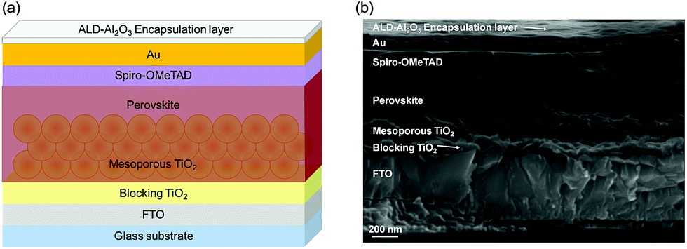 | ||
| Fig. 1 (a) Schematic of the FTO/bl-TiO2/mp-TiO2/MAPbI3/Spiro-OMeTAD/Au architecture with the ALD-Al2O3 encapsulation layer proposed in this work (not to scale). (b) Cross-sectional Scanning Electron Microscopy (SEM) image of a perovskite solar cell containing an ALD-Al2O3 encapsulation layer deposited at 60 °C. | ||
Indeed, after a few minutes of exposure to air, gold surfaces become hydrophobic due to surface adsorption of species in the environment, and surface cleaning pre-treatments such as UV and/or O2 plasma can be applied to improve the quality of the film.91
PSC performance before/after encapsulation and optimization of the deposition temperature
In this work, PSCs were fabricated with minor modifications to the procedure reported by Ahn et al.,83 achieving very similar performances in comparison with the state-of-the-art devices, i.e. efficiencies in the range of 16–18%, with open-circuit voltages (VOC) exceeding 1 V, short-circuit current densities (JSC) over 21 mA cm−2, and fill factors (FF) exceeding 70% with very good reproducibility (see the Ref devices in Fig. S3† and 2c).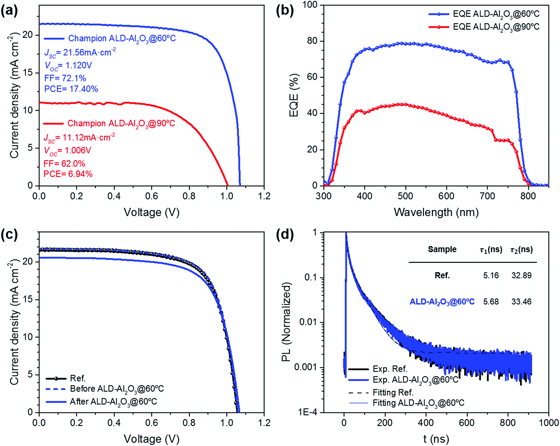 | ||
| Fig. 2 Study of the ALD-Al2O3 encapsulation process at different temperatures. (a) Current density–Voltage (J–V) characteristics for the champion PSCs ALD-Al2O3@90 °C (red) and ALD-Al2O3@60 °C (blue); PV parameters are specified in the legend. (b) External quantum efficiency for the champion PSCs ALD-Al2O3@90 °C (red) and ALD-Al2O3@60 °C (blue). (c) J–V characterization of the ALD-Al2O3@60 °C device with average characteristics before (dashed blue line) and after the encapsulation (solid blue line) process compared with the Ref PSC (black). (d) Time-Resolved Photoluminescence (TRPL) measurements on ALD-Al2O3@60 °C and Ref. | ||
Firstly, to proceed with the encapsulation, an ALD-Al2O3 layer was grown on the top of these PSCs using a deposition temperature of 90 °C inside the ALD reactor. This temperature was prudently chosen by reducing the standard temperature reported for ALD-Al2O3 routines using TMA + H2O (normally set at 130–150 °C71), and slightly decreased for the ALD procedures applied to PSCs (normally fixed at 100 °C), where significant degradation was still observed.72,74,78 In Fig. S2,† the normalized photovoltaic properties (JSC, VOC, FF and PCE) for the encapsulation process at 90 °C and the corresponding reference samples are shown. Reference PSCs before any encapsulation (named as Ref) were taken as a base for the normalized graphs and data.
The Shipment sample, stored in a protective atmosphere and measured again after its return, shows negligible losses (Relative change in PCE amounts to only ∼2.5%), demonstrating sufficient stability of all PV parameters under the shipping conditions used here. For H@90 °C samples, significant performance losses were detected, mainly in photocurrent density (ΔJSC = −36.2%) but also in voltage and fill factor (ΔVOC = −6.5%, ΔFF = −5.1%), resulting in an overall relative decrease in efficiency of ΔPCE = 43.3%. Thus, the heating process at 90 °C inside the ALD reactor during the typical time needed for obtaining an ALD-Al2O3 encapsulation layer is not suitable for a successful and harmless PSC ALD encapsulation. Moreover, for the samples encapsulated at 90 °C (ALD-Al2O3@90 °C), two different trends can be clearly distinguished. One batch of the ALD-Al2O3@90 °C encapsulated devices, around half the samples, exhibited losses very similar to those of H@90 °C, with a total ΔPCE of −53.9%; i.e. primarily a loss in photocurrent (ΔJSC = −37.3%), while the decrease in fill factor detected is slightly higher (ΔFF = −19.6%) than for the H@90 °C samples, without a significant decay in voltage (Table 1 and Fig. S2†). The other batch of ALD-Al2O3@90 °C devices showed critical device failure linked to a pronounced loss in JSC (non-working devices). A priori, we consider this general device failure in non-working devices to be related to a detrimental effect of the precursors (see Fig. S2†), previously observed in the literature72,79 and linked to degradation of the material, since Dong et al. found that when the number of ALD cycles increases, the PbI2 content increases as well.73 Here, we further elaborate on this hypothesis in our XPS section.
| Temperature of ALD-Al2O3 encapsulation | Normalized average variation of PV properties before/after encapsulation | |||
|---|---|---|---|---|
| ΔJSC (%) | ΔVOC (%) | ΔFF (%) | ΔPCE (%) | |
| ALD-Al2O3@90 °C (excluding non-working cells) | −37.3 | −8.1 | −19.6 | −53.9 |
| ALD-Al2O3@60 °C | −3.2 | 0.3 | −3.8 | −6.4 |
To avoid these detrimental effects, we lowered the deposition temperature of the ALD-Al2O3 encapsulation process to 60 °C (ALD-Al2O3@60 °C). The current density–voltage characteristics of the best-performing PSCs after encapsulation in both ALD-Al2O3@90 °C and ALD-Al2O3@60 °C are shown in Fig. 2a. We find an overall performance of 17.40% from the J–V curve for the champion ALD-Al2O3@60 °C sample with JSC = 21.56 mA cm−2, VOC = 1.120 V and FF = 72.1%, practically identical to the performance observed in non-encapsulated samples (Ref). In Fig. 2c, the evolution before/after encapsulation in ALD-Al2O3@60 °C is compared with a Ref cell. The ALD-Al2O3@60 °C process leads to an only very minor reduction in photocurrent in contrast to the encapsulation performed at 90 °C (Fig. 2a and b). Further statistical information is given by the box and whisker diagrams of the PSC characteristics before and after ALD-Al2O3 encapsulation at 60 °C (Fig. S3†), confirming the low dispersion and high reproducibility of the process. In contrast, for the champion ALD-Al2O3@90 °C device, a PCE of only 6.94% was recorded after encapsulation, due to a significant reduction in current as laid out earlier (only JSC = 11.12 mA cm−2) with a reduction in fill factor of up to 62% mainly due to increased series resistance. In summary, we found that the normalized average change of PCE before and after ALD-Al2O3 encapsulation (ΔPCE) was critical for the ALD-Al2O3@90 °C samples resulting in ΔPCE = −53.9%, even after excluding the non-working cells, while the change amounted only to ΔPCE = -6.48% in the case of ALD-Al2O3@60 °C samples (complete information in Table 1). This remarkable performance-maintenance achieved by applying a single ALD coating used as an encapsulation technique for PSCs indicates the key role of temperature control in these procedures.
To further investigate the impact of the ALD-Al2O3 process on the optoelectronic properties of the devices and especially how it affects the charge carrier dynamics, TRPL measurements were carried out. In Fig. 2d, TRPL decays are presented for both Ref and ALD-Al2O3@60 °C samples. The curves were fitted using a biexponential model obtaining very good correlation for both devices at any time interval. Moreover, comparing both models, i.e. for Ref and ALD-Al2O3@60 °C cells, practically identical correlation parameters were obtained. As a result, time constants for rapid (τ1) and slow (τ2) decay processes were similar to reported values11 and almost equivalent between the Ref sample, with τ1 = 5.16 ns and τ2 = 32.89 ns, and the ALD-Al2O3@60 °C sample, with τ1 = 5.68 ns and τ2 = 33.45 ns. This shows that internal mechanisms and carrier dynamics in the PSC are not significantly modified by the 60 °C ALD-Al2O3 encapsulation (more details in the ESI†). Consequently, the ALD-Al2O3@60 °C encapsulation process altered neither the optical nor the transport processes inside the PSC.
Ageing process and stability data
As the innocuousness of the encapsulation procedure (ALD-Al2O3@60 °C) to the PSC performance was demonstrated, we then evaluated the improvement of the long-term stability. Both reference (Ref) and ALD-Al2O3@60 °C devices were kept in an ambient atmosphere without further precautions and repeatedly characterized by J–V measurements. The evolution of the PV properties both for the Ref. and ALD-Al2O3@60 °C devices is compared in Fig. 3a–d. The global evolution of PCE is mostly determined by the FF rather than VOC and JSC. The measured VOC remained high for both types of samples and stayed remarkably constant for the encapsulated devices with an initial VOC of 1.039 V and VOC = 1.038 V after 2256 h of storage. In contrast, for the reference device VOC dropped from 1.090 V to <1 V. In the case of JSC, we observed a linear decrease for the first 1000 hours and subsequent relative stabilization independent of any encapsulation. Curiously, while lowering the ALD deposition temperature was critical to limit JSC losses during the ALD-Al2O3 process, once encapsulated, JSC was a little bit less stable for the ALD-Al2O3 encapsulated samples than for the reference ones. | ||
| Fig. 3 Stability test; evolution of JSC (a), VOC (b), FF (c) and PCE (d) with storage time for Ref (black) and ALD-Al2O3@60 °C (blue). Evolution of hysteresis in Ref (e) and ALD-Al2O3@60 °C (f) devices, before (dotted line) and after 14 days (∼335 h) of ageing under ambient conditions (solid line); for hysteresis measurements, the scan rate was fixed at 20 mV s−1. Hysteresis Index, HI = (PCEreverse − PCEforward)/PCEreverse. (g) Chronopotentiometry of ALD-Al2O3@60 °C under continuous illumination. | ||
However, in both cases the losses were on the same order of magnitude with JSC dropping from 21.57 to 18.19 mA cm−2 for the ALD-Al2O3@60 °C device and from 21.83 to 19.28 mA cm−2 for the reference. Thus, the extension of lifetime in the encapsulated devices is primarily attributed to a stabilization of the fill factor, as in the ALD-Al2O3 protected devices the FF only decreased from 73.4% to 66.4% after 2256 h, while for the reference, it substantially decayed from 75.2% to 34.2%. This FF behavior leads to an overall PCE loss in the case of the reference sample from almost 18% to 6.5% (i.e. 64% of the initial PCE on a normalized scale), whereas ALD-Al2O3@60 °C exhibited a final PCE of 12.4% after more than 2250 hours of storage under ambient conditions (from original PCE = 16.4%), which corresponds to a relative loss of <25% of the initial PCE.
To further elucidate the origin of the differences in the FF decay between the Ref and ALD-Al2O3@60 °C devices, reverse and forward J–V scans were performed for both types of samples to investigate the hysteresis phenomenon immediately after cell fabrication and after ageing (plotted in Fig. 3e–f). In non-encapsulated PSC systems, hysteresis is well known to increase with time,92 which holds true for our reference devices, since the hysteresis index (HI = (PCEreverse − PCEforward)/PCEreverse) was increased from 0.122 to 0.381 after 14 days under ambient conditions. However, in the case of the ALD-Al2O3@60 °C sample, the situation was improved as the typical increase in hysteresis was limited from an initial HI = 0.116 to only 0.192 after 14 days of storage under ambient conditions. An additional chronopotentiometry experiment shown in Fig. 3g reveals that 96.5% of the initial VOC is retained after 33.5 h (in cycles of 0.5 h) under continuous illumination for the ALD-Al2O3@60 °C sample.
Finally, we investigated using XRD whether structural changes occurred in the MAPbI3 films after ∼2250 hours of storage in an ambient atmosphere. Representative XRD patterns of the Ref and ALD-Al2O3@60 °C devices are presented in Fig. 4a. In both cases, diffraction peaks of a tetragonal perovskite phase can be observed at 2θ = 14.1° and 28.4°. However, only in the case of the non-encapsulated device is a peak corresponding to the formation of a PbI2 phase observed at 2θ = 12.6°, which is in agreement with the occurrence of yellow areas visually detected in the aged reference sample, and which has not been witnessed for the samples encapsulated at 60 °C (Fig. 4b). Additional ageing tests at elevated temperatures should be conducted in order to more accurately reflect the operating conditions of the solar cell.
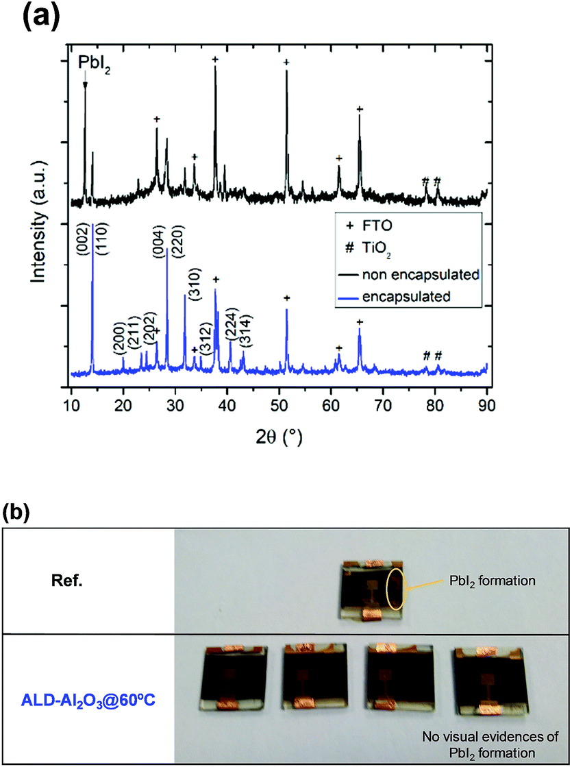 | ||
| Fig. 4 (a) XRD patterns of the Ref (black) and ALD-Al2O3@60 °C (blue) devices stored for ∼2256 h under ambient conditions. Diffraction peaks of FTO and TiO2 are indicated by + and # symbols, respectively. (b) Photograph of the Ref devices on top and ALD-Al2O3@60 °C in the bottom part stored for ∼2256 h (94 days) under ambient conditions. | ||
XPS analysis
To evaluate the formation and impact of the initial Al2O3 ALD layer deposition on the critical material components (MAPbI3 and Spiro-OMeTAD), XPS measurements were performed on glass/FTO/bl-TiO2/mp-TiO2/MAPbI3 and glass/FTO/bl-TiO2/mp-TiO2/MAPbI3/Spiro-OMeTAD (Fig. S5†) samples coated with ALD Al2O3 films of 2 nm nominal thickness, deposited both at 60 °C and 90 °C. This very low thickness allows us to capture the XPS signal of the underlying MAPbI3 and Spiro-OMeTAD layers. We also note that the potential of forming these various interfaces can lead to critical changes in the device functionality.93 First, the presence of the AlOx layer was confirmed by the Al 2p and O 1s contributions in the spectra (74.7 eV and 532.2 eV respectively, Fig. S6†). The AlOx films deposited at 90 °C exhibit a lower concentration of oxygen and carbon, indicative of a higher conversion factor of the ALD precursor. We also show the XPS high-resolution spectra of the Pb 4f, N 1s and I 3d core level regions for the MAPbI3 samples with and without coating by a 2 nm thick Al2O3 layer (Fig. 5). All peaks present one major chemical contribution in good agreement with the literature and notably we do not find any formation of metallic lead evidenced by the absence of any Pb0 contribution in the Pb 4f core level spectra.94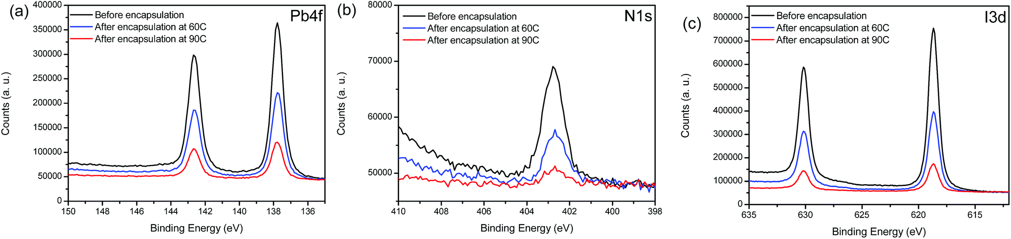 | ||
| Fig. 5 XPS high resolution spectra of the Pb 4f (a), N 1s (b) and I 3d (c) regions for FTO/bl-TiO2/mp-TiO2/MAPbI3 stacks not encapsulated (black), encapsulated at 60 °C with a 2 nm Al2O3 layer (blue) and encapsulated at 90 °C with a 2 nm Al2O3 layer (red). | ||
Furthermore, we do not observe any significant core level shifts in the spectra, which suggests that the respective chemical coordination for all components in the MAPbI3 film is conserved. However, this statement cannot be applied to the carbon component because the C 1s region is convoluted with contributions from the TMA precursor and adventitious carbon (see Fig. S6†). Notably, we do not find any shift of the Fermi level (ΔEF < 0.1 eV) in the MAPbI3 layer, which is in contrast to MAPbI3 interfacing more reactive oxides such as MoO3.95 However, some chemical changes of the MAPbI3 films can be inferred from the elemental ratios (Table 2). Both devices without encapsulation and after a 60 °C encapsulation present similar Pb/I ratios. Indeed, for those two sets of devices, the Pb/I ratio obtained is equal to the theoretical ratio of a MaPbI3 device (0.31 ± 0.03 and 0.34 ± 0.03 respectively). However, an increase of the Pb/I ratio is noted when the deposition is performed at 90 °C. Indeed, the value reaches 0.42 ± 0.03, which suggests that we form a substoichiometric PbI2-rich phase at the interface with the adjacent layer for the high temperature process. Regarding the N/Pb ratio, we observe a decrease for both encapsulation temperatures, leading to values in better agreement with the nominal stoichiometry of the layer. Indeed, the N/Pb ratio for the non-encapsulated device reaches 1.30 ± 0.03 while the nominal stoichiometry is expected to give a ratio of 1.00. The excess in the nitrogen content probably originates from excess MAI in the fabrication process. After contact with the ALD precursors some of the excess MA might be removed, as for the encapsulated devices, the N/Pb ratio is lower (1.19 ± 0.03 and 1.16 ± 0.03 for the encapsulation at 60 °C and 90 °C, respectively). The decomposition of methylammonium has previously been described in the literature.96 Here, in summary the loss in nitrogen for the ALD processing at 60 °C points to a loss of surface excess MA, potentially linked to the interface formation between the AlOx film and MAPbI3, while the concomitant loss of I and N in the case of the 90 °C ALD deposition describes a thorough degradation process.
| Compounds | Before encapsulation | ALD-Al2O3@60 °C (2 nm) | ALD-Al2O3@90 °C (2 nm) |
|---|---|---|---|
| Pb/I | 0.31 ± 0.03 | 0.34 ± 0.03 | 0.42 ± 0.03 |
| N/Pb | 1.30 ± 0.03 | 1.19 ± 0.03 | 1.16 ± 0.03 |
Addressing the differences in the degradation of the Spiro-OMeTAD layer underneath the ALD Al2O3 film is inherently more challenging as carbon and oxygen contributions of the Spiro-OMeTAD molecule to the XPS spectra are convoluted by the contribution of the ALD precursors and adventitious species. Nonetheless, we do see some minor qualitative changes in the carbon signal that are absent in the scans of the AlOx/MAPbI3 interfaces: upon deposition of the AlOx film on top of the Spiro-OMeTAD layer we find a new contribution of C–O bonds at 289 eV binding energy (ESI, Fig. S5†). This C–O component is more pronounced at higher processing temperatures (90 °C) than at lower processing temperatures, indicating a stronger reaction/degradation of the Spiro-OMeTAD surface. Moreover, we find that the N 1s signal of the nitrogen containing moieties in the Spiro-OMeTAD is attenuated to the same degree and remained unchanged for both AlOx overlayers (Fig. S5†). Overall, we conclude from the XPS chemical analysis (full elemental composition in the ESI, Tables S1 and S2†) that the encapsulation performed at 60 °C is more compatible for the full device encapsulation as the chemical integrity of the MAPbI3 layer seems to be better retained.
Conclusions
In summary, we report an efficient method for encapsulation of perovskite solar cells by atomic layer deposition of Al2O3 thin-films. By the careful control of deposition temperatures of the ALD-Al2O3 process, a well-covering continuous encapsulation coating of approximately 16 nm thickness was achieved. In particular, by reducing the ALD-Al2O3 deposition temperature from 90 °C, a typical temperature for this kind of processes, to only 60 °C, we retained over 93% of the initial device efficiency. We attribute this effect to the fact that in the low-temperature process the measured chemical composition and optoelectronic properties relevant for charge collection at the interfaces remain mostly unperturbed, whereas decomposition of the MAPbI3 film into PbI2 sets in for the high temperature ALD process. This demonstrates that our process is compatible with inherently heat sensitive materials used for PSC fabrication, i.e. MAPbI3 and Spiro-OMeTAD. Thus, we project that the results obtained here for our ALD-Al2O3 encapsulation are universally applicable to other and more robust PSC configurations. Finally, we demonstrate that the method is effective in extending the long-term stability since losses in efficiency for the devices encapsulated at 60 °C were limited to <25% of the initial PCE vs. 64% in the case of non-encapsulated devices after >2250 hours of storage under ambient conditions. The reduction in PCE losses is correlated with a better preservation of the fill factor and is accompanied by a mitigation of hysteresis. We ultimately link this improvement to the suppression of PbI2 formation in the encapsulated devices. Hence, our method provides a new encapsulation route which not only extends the lifetime of PSCs for lab applications but also paves the way for future commercialization efforts.Conflicts of interest
There are no conflicts to declare.Acknowledgements
This work was partly carried out in the framework of a project of IPVF, which has been supported by the French Government in the frame of the program of investment for the future (Programme d’Investissement d’Avenir ANR-IEED-002-01). P.S. thanks the French Agence Nationale de la Recherche for funding under the contract number ANR-17-MPGA-0012.References
- A. Kojima, K. Teshima, Y. Shirai and T. Miyasaka, J. Am. Chem. Soc., 2009, 131, 6050–6051 CrossRef PubMed.
- J. Burschka, N. Pellet, S.-J. Moon, R. Humphry-Baker, P. Gao, M. K. Nazeeruddin and M. Grätzel, Nature, 2013, 499, 316–319 CrossRef PubMed.
- M. M. Lee, J. Teuscher, T. Miyasaka, T. N. Murakami and H. J. Snaith, Sci. 80, 2012, 338, 643–647 CrossRef PubMed.
- N. J. Jeon, J. H. Noh, Y. C. Kim, W. S. Yang, S. Ryu and S. Il Seok, Nat. Mater., 2014, 13, 897–903 CrossRef PubMed.
- N. J. Jeon, J. H. Noh, W. S. Yang, Y. C. Kim, S. Ryu, J. Seo and S. Il Seok, Nature, 2015, 517, 476–480 CrossRef PubMed.
- S. Colella, E. Mosconi, P. Fedeli, A. Listorti, F. Gazza, F. Orlandi, P. Ferro, T. Besagni, A. Rizzo, G. Calestani, G. Gigli, F. De Angelis and R. Mosca, Chem. Mater., 2013, 25, 4613–4618 CrossRef.
- Q. Lin, A. Armin, R. Chandra, R. Nagiri, P. L. Burn and P. Meredith, Nat. Photonics, 2015, 9, 106–112 CrossRef.
- E. M. Hutter, M. C. Gélvez-Rueda, A. Osherov, V. Bulović, F. C. Grozema, S. D. Stranks and T. J. Savenije, Nat. Mater., 2016, 16, 115–120 CrossRef PubMed.
- J. H. Heo, S. H. Im, J. H. Noh, T. N. Mandal, C.-S. Lim, J. A. Chang, Y. H. Lee, H. Kim, A. Sarkar, M. K. Nazeeruddin, M. Graetzel and S. Il Seok, Nat. Photonics, 2013, 7, 486–491 CrossRef.
- E. Guillén, F. J. Ramos, J. A. Anta and S. Ahmad, J. Phys. Chem. C, 2014, 118, 22913–22922 CrossRef.
- S. D. Stranks, G. E. Eperon, G. Grancini, C. Menelaou, M. J. P. Alcocer, T. Leijtens, L. M. Herz, A. Petrozza and H. J. Snaith, Sci. 80, 2013, 342, 341–344 CrossRef PubMed.
- Q. Chen, H. Zhou, Z. Hong, S. Luo, H.-S. Duan, H.-H. Wang, Y. Liu, G. Li and Y. Yang, J. Am. Chem. Soc., 2014, 136, 622–625 CrossRef PubMed.
- G. Longo, L. Gil-Escrig, M. J. Degen, M. Sessolo and H. J. Bolink, Chem. Commun., 2015, 7376–7378 RSC.
- A. Mei, X. Li, L. Liu, Z. Ku, T. Liu, Y. Rong, M. Xu, M. Hu, J. Chen, Y. Yang, M. Gratzel and H. Han, Sci. 80, 2014, 345, 295–298 CrossRef PubMed.
- M. Liu, M. B. Johnston and H. J. Snaith, Nature, 2013, 501, 395–398 CrossRef PubMed.
- Z. Yu and L. Sun, Adv. Energy Mater., 2015, 5, 1500213 CrossRef.
- L. Meng, J. You, T.-F. Guo and Y. Yang, Acc. Chem. Res., 2015, 49, 155–165 CrossRef PubMed.
- S. T. Williams, A. Rajagopal, C. Chueh and A. K. Y. Jen, J. Phys. Chem. Lett., 2016, 7, 811–819 CrossRef PubMed.
- Z. Wang, Z. Shi, T. Li, Y. Chen and W. Huang, Angew. Chem., Int. Ed., 2017, 56, 1190–1212 CrossRef PubMed.
- J. Chen, X. Cai, D. Yang, D. Song, J. Wang, J. Jiang, A. Ma, S. Lv, M. Z. Hu and C. Ni, J. Power Sources, 2017, 355, 98–133 CrossRef.
- J. A. Christians, P. Schulz, J. S. Tinkham, T. H. Schloemer, S. P. Harvey, B. J. Tremolet de Villers, A. Sellinger, J. J. Berry and J. M. Luther, Nat. Energy, 2018, 3, 68–74 CrossRef.
- X. Wu, M. T. Trinh, D. Niesner, H. Zhu, Z. Norman, J. S. Owen, O. Yaffe, B. J. Kudisch and X. Zhu, J. Am. Chem. Soc., 2015, 137, 2089–2096 CrossRef PubMed.
- C. Eames, J. M. Frost, P. R. F. Barnes, B. C. O'Regan, A. Walsh and M. S. Islam, Nat. Commun., 2015, 6, 7497 CrossRef PubMed.
- J. M. Azpiroz, E. Mosconi, J. Bisquert and F. De Angelis, Energy Environ. Sci., 2015, 8, 2118–2127 RSC.
- B. Conings, J. Drijkoningen, N. Gauquelin, A. Babayigit, J. D'Haen, L. D'Olieslaeger, A. Ethirajan, J. Verbeeck, J. Manca, E. Mosconi, F. De Angelis and H. Boyen, Adv. Energy Mater., 2015, 5, 1500477 CrossRef.
- N.-K. Kim, Y. H. Min, S. Noh, E. Cho, G. Jeong, M. Joo, S.-W. Ahn, J. S. Lee, S. Kim, K. Ihm, H. Ahn, Y. Kang, H.-S. Lee and D. Kim, Sci. Rep., 2017, 7, 4645 CrossRef PubMed.
- T. Leijtens, G. E. Eperon, S. Pathak, A. Abate, M. M. Lee and H. J. Snaith, Nat. Commun., 2013, 4, 2885 CrossRef PubMed.
- N. Klein-Kedem, D. Cahen and G. Hodes, Acc. Chem. Res., 2016, 49, 347–354 CrossRef PubMed.
- D. W. DeQuilettes, W. Zhang, V. M. Burlakov, D. J. Graham, T. Leijtens, A. Osherov, V. Bulović, H. J. Snaith, D. S. Ginger and S. D. Stranks, Nat. Commun., 2016, 7, 11683 CrossRef PubMed.
- T.-Y. Yang, G. Gregori, N. Pellet, M. Grätzel and J. Maier, Angew. Chem., Int. Ed., 2015, 54, 7905–7910 CrossRef PubMed.
- A. Leguy, Y. Hu, M. Campoy-quiles, M. I. Alonso, O. J. Weber, P. Azarhoosh, M. Van Schilfgaarde, M. T. Weller, T. Bein, J. Nelson, P. Docampo and P. R. F. Barnes, Chem. Mater., 2015, 27, 3397–3407 CrossRef.
- J. Yang, B. D. Siempelkamp, D. Liu and T. L. Kelly, ACS Nano, 2015, 9, 1955–1963 CrossRef PubMed.
- D. Li, S. A. Bretschneider, V. W. Bergmann, I. M. Hermes, J. Mars, A. Klasen, H. Lu, W. Tremel, M. Mezger, H. J. Butt, S. A. L. Weber and R. Berger, J. Phys. Chem. C, 2016, 120, 6363–6368 CrossRef.
- N. Aristidou, I. Sanchez-Molina, T. Chotchuangchutchaval, M. Brown, L. Martinez, T. Rath and S. A. Haque, Angew. Chem., Int. Ed., 2015, 54, 8208–8212 CrossRef PubMed.
- N. Li, Z. Zhu, C. C. Chueh, H. Liu, B. Peng, A. Petrone, X. Li, L. Wang and A. K. Y. Jen, Adv. Energy Mater., 2017, 7, 1601307 CrossRef.
- M. Saliba, T. Matsui, J.-Y. Seo, K. Domanski, J.-P. Correa-Baena, M. K. Nazeeruddin, S. M. Zakeeruddin, W. Tress, A. Abate, A. Hagfeldt and M. Grätzel, Energy Environ. Sci., 2016, 9, 1989–1997 RSC.
- Z. Li, M. Yang, J. S. Park, S. H. Wei, J. J. Berry and K. Zhu, Chem. Mater., 2016, 28, 284–292 CrossRef.
- H. Tsai, W. Nie, J.-C. Blancon, C. C. Stoumpos, R. Asadpour, B. Harutyunyan, A. J. Neukirch, R. Verduzco, J. J. Crochet, S. Tretiak, L. Pedesseau, J. Even, M. A. Alam, G. Gupta, J. Lou, P. M. Ajayan, M. J. Bedzyk, M. G. Kanatzidis and A. D. Mohite, Nature, 2016, 536, 312–316 CrossRef PubMed.
- M. Salado, F. J. Ramos, V. M. Manzanares, P. Gao, M. K. Nazeeruddin, P. J. Dyson and S. Ahmad, ChemSusChem, 2016, 9, 2708–2714 CrossRef PubMed.
- F. J. Ramos, M. Oliva-Ramirez, M. K. Nazeeruddin, M. Grätzel, A. R. Gonzalez-Elipe and S. Ahmad, J. Mater. Chem. A, 2015, 3, 13291–13298 RSC.
- A. Mei, X. Li, L. Liu, Z. Ku, T. Liu, Y. Rong, M. Xu, M. Hu, J. Chen, Y. Yang, M. Gratzel and H. Han, Sci. 80, 2014, 345, 295–298 CrossRef PubMed.
- H. Tan, A. Jain, O. Voznyy, X. Lan, F. P. García de Arquer, J. Z. Fan, R. Quintero-Bermudez, M. Yuan, B. Zhang, Y. Zhao, F. Fan, P. Li, L. N. Quan, Y. Zhao, Z.-H. Lu, Z. Yang, S. Hoogland and E. H. Sargent, Sci. 80, 2017, 355, 722–726 CrossRef PubMed.
- Y. H. Lee, J. Luo, M. K. Son, P. Gao, K. T. Cho, J. Seo, S. M. Zakeeruddin, M. Grätzel and M. K. Nazeeruddin, Adv. Mater., 2016, 28, 3966–3972 CrossRef PubMed.
- J. P. Correa Baena, L. Steier, W. Tress, M. Saliba, S. Neutzner, T. Matsui, F. Giordano, T. J. Jacobsson, A. R. Srimath Kandada, S. M. Zakeeruddin, A. Petrozza, A. Abate, M. K. Nazeeruddin, M. Grätzel and A. Hagfeldt, Energy Environ. Sci., 2015, 8, 2928–2934 RSC.
- J. You, L. Meng, T.-B. Song, T.-F. Guo, Y. (Michael) Yang, W.-H. Chang, Z. Hong, H. Chen, H. Zhou, Q. Chen, Y. Liu, N. De Marco and Y. Yang, Nat. Nanotechnol., 2016, 11, 75–81 CrossRef PubMed.
- L. Calió, S. Kazim, M. Grätzel and S. Ahmad, Angew. Chem., Int. Ed., 2016, 55, 14522–14545 CrossRef PubMed.
- T. Leijtens, I. Ding, T. Giovenzana, J. T. Bloking, M. D. Mcgehee and A. Sellinger, ACS Nano, 2012, 6, 1455–1462 CrossRef PubMed.
- K. Domanski, J.-P. Correa-Baena, N. Mine, M. K. Nazeeruddin, A. Abate, M. Saliba, W. Tress, A. Hagfeldt and M. Grätzel, ACS Nano, 2016, 10, 6306–6314 CrossRef PubMed.
- A. Poglitsch and D. Weber, J. Chem. Phys., 1987, 87, 6373–6378 CrossRef.
- F. J. Ramos, D. Cortes, A. Aguirre, F. J. Castano and S. Ahmad, IEEE 40th PVSC, 2014, 2584–2587 Search PubMed.
- H. C. Weerasinghe, Y. Dkhissi, A. D. Scully, R. A. Caruso and Y. B. Cheng, Nano Energy, 2015, 18, 118–125 CrossRef.
- L. Shi, T. L. Young, J. Kim, Y. Sheng, L. Wang, Y. Chen, Z. Feng, M. J. Keevers, X. Hao, P. J. Verlinden, M. A. Green and A. W. Y. Ho-Baillie, ACS Appl. Mater. Interfaces, 2017, 9, 25073–25081 CrossRef PubMed.
- R. Cheacharoen, N. J. Rolston, D. Harwood, K. A. Bush, R. H. Dauskardt and M. D. McGehee, Energy Environ. Sci., 2018, 11, 144–150 RSC.
- A. Hinsch, S. Mastroianni, H. Brandt, F. Heinz, M. C. Schubert and W. Veurman, 29th Eur. PV Sol. Energy Conf. Exhib., 2014, pp. 1–5 Search PubMed.
- D. B. Khadka, Y. Shirai, M. Yanagida and K. Miyano, J. Mater. Chem. C, 2018, 6, 162–170 RSC.
- Q. Dong, F. Liu, M. K. Wong, H. W. Tam, A. B. Djurišić, A. Ng, C. Surya, W. K. Chan and A. M. C. Ng, ChemSusChem, 2016, 9, 2597–2603 CrossRef PubMed.
- F. Matteocci, L. Cinà, E. Lamanna, S. Cacovich, G. Divitini, P. A. Midgley, C. Ducati and A. Di Carlo, Nano Energy, 2016, 30, 162–172 CrossRef.
- F. Bella, G. Griffini, J.-P. Correa-Baena, G. Saracco, M. Grätzel, A. Hagfeldt, S. Turri and C. Gerbaldi, Sci. 80, 2016, 354, 203–206 CrossRef PubMed.
- I. Hwang, I. Jeong, J. Lee, M. J. Ko and K. Yong, ACS Appl. Mater. Interfaces, 2015, 7, 17330–17336 CrossRef PubMed.
- S. M. George, Chem. Rev., 2010, 110, 111–131 CrossRef PubMed.
- X. Meng, X. Wang, D. Geng, C. Ozgit-Akgun, N. Schneider and J. W. Elam, Mater. Horiz., 2017, 4, 133–154 RSC.
- V. Zardetto, B. L. Williams, A. Perrotta, F. Di Giacomo, M. A. Verheijen, R. Andriessen, W. M. M. Kessels and M. Creatore, Sustainable Energy Fuels, 2017, 1, 30–55 RSC.
- J. Meyer, P. Görrn, F. Bertram, S. Hamwi, T. Winkler, H.-H. Johannes, T. Weimann, P. Hinze, T. Riedl and W. Kowalsky, Adv. Mater., 2009, 21, 1845–1849 CrossRef.
- S.-W. Seo, E. Jung, H. Chae and S. M. Cho, Org. Electron., 2012, 13, 2436–2441 CrossRef.
- K. Bouzid, T. Maindron and H. Kanaan, J. Soc. Inf. Disp., 2016, 24, 563–568 CrossRef.
- I. S. Kim, D. H. Cao, D. B. Buchholz, J. D. Emery, O. K. Farha, J. T. Hupp, M. G. Kanatzidis and A. B. F. Martinson, Nano Lett., 2016, 16, 7786–7790 CrossRef PubMed.
- K. O. Brinkmann, J. Zhao, N. Pourdavoud, T. Becker, T. Hu, S. Olthof, K. Meerholz, L. Hoffmann, T. Gahlmann, R. Heiderhoff, M. F. Oszajca, N. A. Luechinger, D. Rogalla, Y. Chen, B. Cheng and T. Riedl, Nat. Commun., 2017, 8, 13938 CrossRef PubMed.
- C.-Y. Chang, C.-T. Chou, Y.-J. Lee, M.-J. Chen and F.-Y. Tsai, Org. Electron., 2009, 10, 1300–1306 CrossRef.
- H. Goverde, B. Vermang, A. Morato, J. John, J. Horzel, G. Meneghesso and J. Poortmans, Energy Procedia, 2012, 27, 355–360 CrossRef.
- L. C. Wang, Y. Y. Han, K. C. Yang, M. J. Chen, H. C. Lin, C. K. Lin and Y. T. Hsu, Surf. Coat. Technol., 2016, 305, 158–164 CrossRef.
- R. L. Puurunen, J. Appl. Phys., 2005, 97, 121301 CrossRef.
- I. S. Kim and A. B. F. Martinson, J. Mater. Chem. A, 2015, 3, 20092–20096 RSC.
- X. Dong, X. Fang, M. Lv, B. Lin, S. Zhang, J. Ding and N. Yuan, J. Mater. Chem. A, 2015, 3, 5360–5367 RSC.
- D. Koushik, W. J. H. Verhees, Y. Kuang, S. Veenstra, D. Zhang, M. A. Verheijen, M. Creatore and R. E. I. Schropp, Energy Environ. Sci., 2017, 10, 91–100 RSC.
- M. Kot, C. Das, Z. Wang, K. Henkel, Z. Rouissi, K. Wojciechowski, H. J. Snaith and D. Schmeisser, ChemSusChem, 2016, 9, 3401–3406 CrossRef PubMed.
- T. Maindron, B. Aventurier, A. Ghazouani, T. Jullien, N. Rochat, J.-Y. Simon and E. Viasnoff, Thin Solid Films, 2013, 548, 517–525 CrossRef.
- P. F. Carcia, R. S. McLean, M. D. Groner, A. A. Dameron and S. M. George, J. Appl. Phys., 2009, 106, 23533 CrossRef.
- C. Y. Chang, K. T. Lee, W. K. Huang, H. Y. Siao and Y. C. Chang, Chem. Mater., 2015, 27, 5122–5130 CrossRef.
- Y. Il Lee, N. J. Jeon, B. J. Kim, H. Shim, T. Y. Yang, S. Il Seok, J. Seo and S. G. Im, Adv. Energy Mater., 2017, 1701928 Search PubMed.
- J. D. Affinito, M. E. Gross, C. A. Coronado, G. L. Graff, I. N. Greenwell and P. M. Martin, Thin Solid Films, 1996, 290–291, 63–67 CrossRef.
- J. S. Park, H. Chae, H. K. Chung and S. I. Lee, Semicond. Sci. Technol., 2011, 26, 34001 CrossRef.
- T. Maindron, T. Jullien and A. André, J. Vac. Sci. Technol., A, 2016, 34, 31513 CrossRef.
- N. Ahn, D.-Y. Son, I.-H. Jang, S. M. Kang, M. Choi and N.-G. Park, J. Am. Chem. Soc., 2015, 137, 8696–8699 CrossRef PubMed.
- ASTM Standard E902, 82, ‘Practice for Checking the Operating Characteristics of X-Ray Photoelectron Spectrometers’, ASTM International, West Conshohocken, PA, 1994 Search PubMed.
- A. C. Dillon, A. W. Ott, J. D. Way and S. M. George, Surf. Sci., 1995, 322, 230–242 CrossRef.
- A. Rahtu, T. Alaranta and M. Ritala, Langmuir, 2001, 17, 6506–6509 CrossRef.
- J. Lu, B. Liu, N. P. Guisinger, P. C. Stair, J. P. Greeley and J. W. Elam, Chem. Mater., 2014, 26, 6752–6761 CrossRef.
- M. D. Detwiler, A. Gharachorlou, L. Mayr, X.-K. Gu, B. Liu, J. Greeley, W. N. Delgass, F. H. Ribeiro and D. Y. Zemlyanov, J. Phys. Chem. C, 2015, 119, 2399–2411 Search PubMed.
- L. Qian, W. Shen, B. Shen, G. W. Qin and B. Das, Nanotechnology, 2010, 21, 305705 CrossRef PubMed.
- M. M. Biener, J. Biener, A. Wichmann, A. Wittstock, T. F. Baumann, M. Bäumer and A. V. Hamza, Nano Lett., 2011, 11, 3085–3090 CrossRef PubMed.
- C. A. Lancaster and J. S. Shumaker-Parry, Thin Solid Films, 2016, 612, 141–146 CrossRef.
- K. Domanski, E. A. Alharbi, A. Hagfeldt, M. Grätzel and W. Tress, Nat. Energy, 2018, 3, 61–67 CrossRef.
- P. Schulz, ACS Energy Lett., 2018, 3, 1287–1293 CrossRef.
- C. Rocks, V. Svrcek, P. Maguire and D. Mariotti, J. Mater. Chem. C, 2017, 5, 902–916 RSC.
- P. Schulz, J. O. Tiepelt, J. A. Christians, I. Levine, E. Edri, E. M. Sanehira, G. Hodes, D. Cahen and A. Kahn, ACS Appl. Mater. Interfaces, 2016, 8, 31491–31499 CrossRef PubMed.
- K. X. Steirer, P. Schulz, G. Teeter, V. Stevanovic, M. Yang, K. Zhu and J. J. Berry, ACS Energy Lett., 2016, 1, 360–366 CrossRef.
Footnote |
| † Electronic supplementary information (ESI) available. See DOI: 10.1039/c8se00282g |
| This journal is © The Royal Society of Chemistry 2018 |