
 Open Access Article
 This Open Access Article is licensed under a Creative Commons Attribution-Non Commercial 3.0 Unported Licence
Plasmon enhanced fluorescence from meticulously positioned gold nanoparticles, deposited by ultra sonic spray coating on organic light emitting diodes†
Rachith Shanivarasanthe
Nithyananda Kumar
 *ab,
Maarten
Eerdekens
c,
Yovan
de Coene
c,
Veda Sandeep
Nagaraja
d,
Shabnam
Ahadzadeh
ab,
Melissa
Van landeghem
ab,
Thierry
Verbiest
c and
Wim
Deferme
*ab
*ab,
Maarten
Eerdekens
c,
Yovan
de Coene
c,
Veda Sandeep
Nagaraja
d,
Shabnam
Ahadzadeh
ab,
Melissa
Van landeghem
ab,
Thierry
Verbiest
c and
Wim
Deferme
*ab
aUHasselt – Hasselt University, Institute for Materials Research (IMO-IMOMEC), Agoralaan 1, Diepenbeek, 3590, Belgium. E-mail: rachith.shanivarasanthe@uhasselt.be; wim.deferme@uhasselt.be
bIMOMEC Division, IMEC, Wetenschapspark 1, Diepenbeek, 3590, Belgium
cMolecular Imaging and Photonics, Celestijnenlaan 200D, 3001 Leuven, Belgium
dTyndall National Institute, Micro Nano Systems centre, Ireland
First published on 9th February 2023
Abstract
Enhancement of the spontaneous emission of fluorophores aided by plasmonic nanoparticles (PNPs) prompts the growth of plasmonic organic light emitting diodes (OLEDs). Together with the spatial dependence of the fluorophore and PNPs on enhanced fluorescence, the surface coverage of the PNPs controls the charge transport in OLEDs. Hence, here, the spatial and surface coverage reliance of plasmonic gold nanoparticles is controlled by a roll-to-roll compatible ultrasonic spray coating technique. A 2-fold enhancement in the multi photon fluorescence is seen by two-photon fluorescence microscopy for a polystyrene sulfonate (PSS) stabilized gold nanoparticle located 10 nm away from the super yellow fluorophore. Fluorescence enhancement combined with ∼2% surface coverage of PNPs, provides a 33%, 20% and ∼40% increase in the electroluminescence, luminous efficacy and external quantum efficiency, respectively.
Introduction
Since Drexhage observed the impact of the interface on the decay of fluorescence,1 extensive research on the fundamentals2–5 and applications6,7 of this impact have propelled the field greatly. Initially explored as a spectroscopy method, fluorescence decay gradually found its feet in optoelectronics, especially in the field of photovoltaics, light emission, and photodetectors. This is made possible due to the introduction of plasmon enhanced fluorescence (PEF), where the presence of a metal interface impacts the transition between two quantum states. This transition, depending on the distance, could amplify the fluorescence or induce metal enhanced quenching. In optoelectronics device architecture, the place of the metal electrodes cannot be changed at will. In the case of plasmonic nanoparticles, however, the said transition can be altered on demand because of the versatility of the nanoparticles that can be incorporated inside the device architecture without affecting its electronic and optical properties. Plasmonic nanoparticles act as nanoantenna upon resonantly coupling with the electromagnetic waves (Fig. 1a).8 This concentrates the electromagnetic field of the incoming light onto the surface of the plasmonic nanoparticles (PNPs). The confined field leads to increased light absorption by the material close to the PNPs,8 and modifies the decay pathways through the generated near field, which alters the quantum yield of the materials. The impact of the near field, E, on the transition rate of the quantum state is given by the Fermi golden rule,9–11| γex = (4π2)/ℏ|〈e|E·p|g〉|2ρe | (1) |
| Q = k/(k + knr) | (2) |
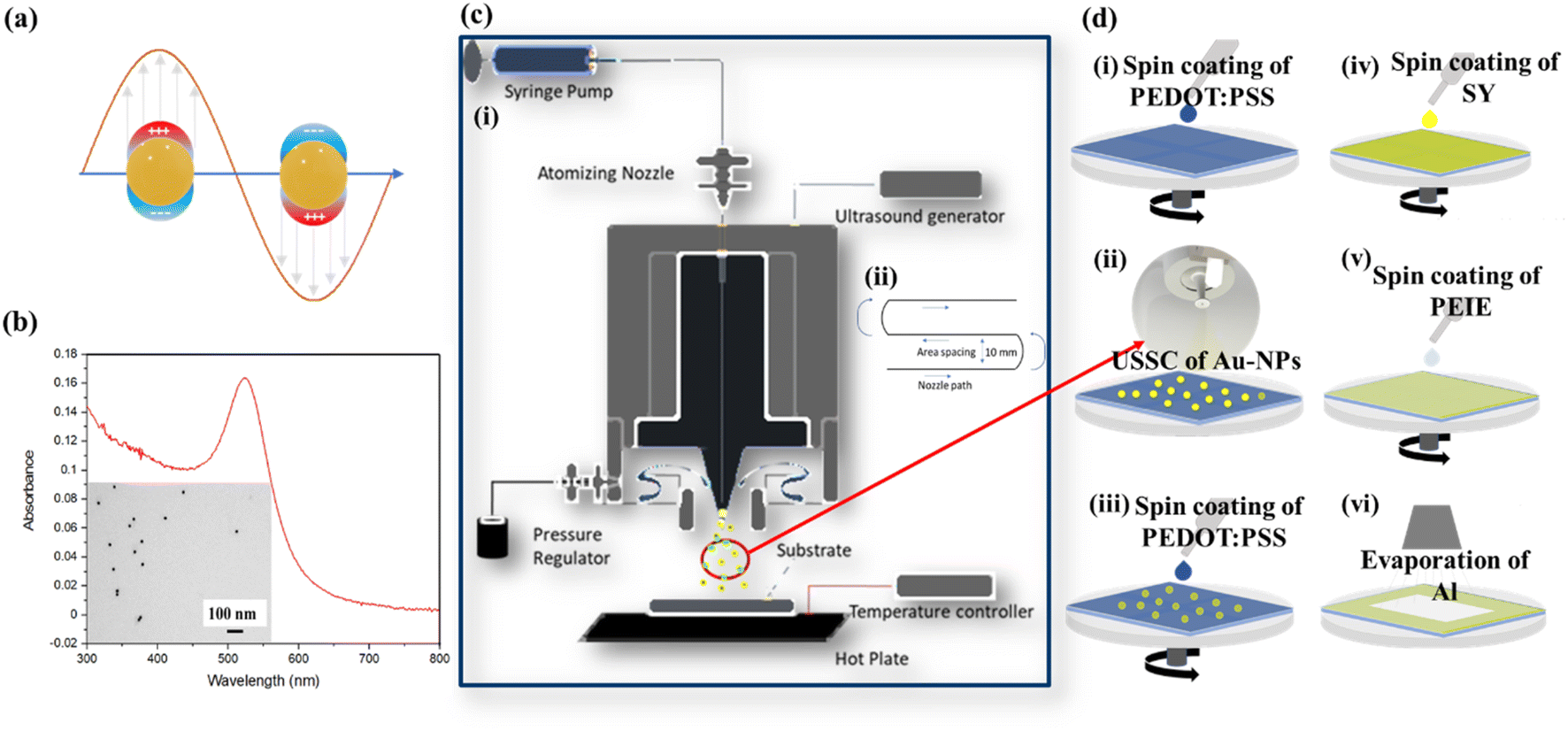 | ||
| Fig. 1 (a) Graphical representation of the localized plasmon resonance of the PNPs upon excitation with EM radiation. (b) UV-Vis spectrum of the synthesized Au-NPs showing a plasmon peak at 520 nm. Inset: TEM image of 15 nm diameter spherical Au-NPs. Deposition of Au-NPs using USSC. (c) Schematic representation of the fabrication technology used: (i) ultrasonic spray coating set up. (ii) Nozzle path of the USSC. (d) Fabrication steps incorporating the Au-NPs onto the OLEDs: (i) spin coating of PEDOT:PSS as the hole injection layer. (ii) USSC of Au-NPs. (iii) Spin coating of PEDOT:PSS to vary the gap between the Au-NPs and active layer. (iv) Spin coating of super yellow as an active layer. (v) Spin coating of PEIE as electron injection layer. (vi) Thermal evaporation of aluminium as the cathode. | ||
To tackle these challenges, polystyrene sulfonate stabilised spherical gold nanoparticles (15 nm) are synthesized for this study. Gold nanoparticles are selected because of their unique properties like higher chemical, physical and photo-stability, easily polarizable conduction electrons, ease of amplifying the EM field on the nanometre scale, and a multitude of optical properties related to surface plasmons. The 15 nm size of the nanoparticle is chosen based on the superior absorption cross-section compared to the scattering cross-section, also the localized surface plasmon resonance of these nanoparticles in a poly(3,4-ethylenedioxythiophene) polystryrene sulfonate (PEDOT:PSS) surrounding medium redshifts to 548 nm, which closely matches with the super yellow light emission. The choice of polystyrene sulfonate as a stabilizer is to favour the electronic properties of the organic semiconducting layers like PEDOT:PSS. For an OLED device architecture of ITO/PEDOT:PSS/SY/PEIE/AL, (where SY = super yellow, PEIE = polyethylenimine ethoxylated solution, AL = active layer) polystyrene sulfonate stabilised gold nanoparticles were deposited inside the PEDOT:PSS at a required surface coverage to optimize fluorescence and to minimize the charge blocking by field coupling of Au-NPs.
The spatial dependence of plasmon enhanced fluorescence was investigated by depositing the Au-NPs at different distances from the active layer using roll-to-roll compatible ultrasonic spray coating technology (USSC). USSC has shown its versatility in depositing thin films for solar cells,46–49 organic light-emitting diodes50 and sensors51 with the added advantage of achieving minimum material waste. There are several techniques to study plasmon-enhanced fluorescence such as fluorescence-lifetime imaging microscopy,52 ultra-high time-resolved fluorescence spectroscopy,53 time-correlated single-photon counting,54 tip-enhanced Raman spectroscopy,55 shell-isolated nanoparticle enhanced fluorescence,56 shell-isolated nanoparticle enhanced Raman scattering,57 tip-enhanced near-field optical microscopy58 and multi photon fluorescence.58 Two-photon fluorescence (2PF) is more sensitive and provides a more favourable signal-to-noise ratio59 resulting in lower measurement errors. Also, the photobleaching is low with 2PF compared with one photon measurement systems,60 and the 2PF measurement system can perform a Z-scan, i.e. can excite the plasmonic nanoparticle locally and hence eliminate the signal emanating from the surrounding matrix. Compared to time resolved photoluminescence, the 2PF showcases key advantages: (a) it allows for the study of nanoparticles buried deep inside the layers, as the excitation of fluorescence occurs at longer wavelengths where the absorption of light by these layers is lower at longer wavelengths; (b) since the excitation of fluorescence occurs at a very specific location within the sample, the two-photon fluorescence measurements allows for more precise imaging of small structures and processes therefore it has higher spatial resolution than TRPL decay measurements.
Therefore, in the present work, at first, extensive simulations are performed to investigate the influence of near field enhancement, and localized surface plasmon resonance for different sizes of the nanoparticles in different surrounding mediums. This is followed by depositing the Au-NPs at the required surface coverage using the USSC. Later the PEF from the Au-NPs embedded architecture is for the first time investigated by 2PF and the effect of PEF over the OLED performance parameters is investigated in detail. The use of USSC to deposit the Au-NPs at will, and the ease of investigating the PEF in an Au-NPs incorporated organic optoelectronic device by 2PF, provide an innovative and faster way to study the performance enhancement of PNP embedded organic optoelectronic devices. The optimized surface coverage of the PSS stabilized Au-NPs for glass/Au-NPs/(with or without) PEDOT:PSS/SY architecture, resulted in a 2-fold enhancement in the multi photon fluorescence. When the same scheme is incorporated into the complete OLED architecture of glass/ITO/PEDOT:PSS/Au-NPs/PEDOT:PSS/SY/PEIE/AL, the OLED’s electroluminescence, external quantum efficiency, illuminance and luminous efficacy are uplifted significantly compared to the standard devices without nanoparticles.
Materials and methods
Materials
Gold(III) chloride hydrate (HAuCl4), sodium citrate (Na citr.), poly(ethylene glycol)methyl ether thiol (avg. MW 800) (PEGMET) and poly styrenesulfonate (avg MW = 4300) (PSS) were purchased from Sigma. ITO coated glass substrates were purchased from BIOTAIN Hongkong co. limited (thickness 135 nm ± 5 nm, with a resistance of 10–15 Ωq−1 with a transmittance of >85%). Poly(3,4-ethylenedioxythiophene) polystyrene sulfonate (PEDOT:PSS, grade Al 4083) was purchased from Heraeus. Super yellow light emitting PPV copolymer (SY), polyethylenimine, 80% ethoxylated solution (PEIE, 37% wt% in H2O) were purchased from Aldrich.Synthesis of PSS stabilized Au-NPs
The plasmonic Au-NPs were synthesized using the Turkevic method,61–63 and for PSS stabilization, 0.250 g PSS was added to 50 ml AuNP solution and shaken for 2 h. The mixture was then centrifuged at 15![[thin space (1/6-em)]](https://www.rsc.org/images/entities/char_2009.gif) 000 rpm for 30 min, removing as much of the supernatant as possible, the precipitate was then redissolved in 50 ml water and vortexed for 1 min. This procedure was repeated one more time.
000 rpm for 30 min, removing as much of the supernatant as possible, the precipitate was then redissolved in 50 ml water and vortexed for 1 min. This procedure was repeated one more time.
Fabrication of devices for 2PF
To investigate the influence of PNPs on fluorescence enhancement, three sets of samples are prepared. One without PNPs where only the active layer super yellow (SY) is spin coated (STD sample). In a second set, the PNPs are deposited on a glass substrate using USSC (details of USSC and ink preparation of the PNPs are given in other sections of the Materials and methods section) followed by spin coating of SY. The third sample consists of USSC of PNPs on the glass substrate, followed by spin coating of 10 nm PEDOT:PSS, followed by spin coating of SY.Fabrication of standard OLEDs
The super yellow (SY) solution was prepared inside a glove box by adding 20 mg of SY light emitting PPV copolymer, onto 4 ml of chlorobenzene and then stirring vigorously overnight at 50 °C. PEIE solutions were prepared from 0.1 ml of polyethylenimine, 80% ethoxylated in 35 ml of IPA and stirred for 2 min. Pre-patterned ITO substrates were thoroughly rinsed using acetone to eliminate the leftover organic substance resulting from the removal of plastic encapsulation on the ITO substrate. The substrates were rinsed in soap solution before the 30 min ultra-sonification in a soap solution, followed by ultra-sonification in deionized water for 20 min, and acetone and isopropanol alcohol (IPA) for 10 min each. Later the substrates were dried with compressed nitrogen. Finally, 30 min of exposure to UV and ozone completes the cleaning procedure.Using a chromafil 0.45 μm filter, 40 nm PEDOT:PSS is spin-coated onto the ITO substrate at 3000 rpm. The substrates were then annealed for 15 min at 130 °C under atmosphere to completely dry the film and reduce the free volume between the polymer chain and hence increase the crystallinity and mechanical stabilization of the polymer. The samples were then sent to a nitrogen-filled glove box maintained under O2 at less than 0.1 ppm and H2O less than 0.1 ppm, where the active material, 80 nm SY is spin-coated at 750 rpm. These substrates were then annealed at 50 °C for 10 min. This is followed by a spin coating of 10 nm PEIE at 2000 rpm. Later, the samples were transferred into an evaporation chamber where 80 nm of aluminium is thermally evaporated at an evaporation rate of 0.2 Å s−1.
Fabrication of Au-NPs incorporated OLEDs
The fabrication of Au-NPs incorporated OLEDs is almost the same as the way standard OLEDs are made, however, instead of pure PEDOT:PSS, a sandwich structure containing PEDOT:PSS/Au-NPs/PEDOT:PSS (total 40 nm) is fabricated on ITO substrates. PEDOT:PSS is spin coated whereas the Au-NPs are deposited by USSC, here, the thickness of PEDOT:PSS is varied to change the vertical position of the Au-NPs from the active layer.Ink formulation for USSC
For ultrasonic spray coating, different solutions containing 2, 4, 8, 12, 16 and 20 ml of Au-NPs in 40 ml of IPA were ultrasonicated for 20 min before the ultrasonic spray coating. 8 ml Au-NPs in 40 ml of IPA gave an optimized result and hence surface coverage is varied by varying the number of passes of 8 ml Au-NPs in 40 ml of IPA.Ultrasonic spray coating
A spray coater from Sono-Tek corporation, equipped with an impact nozzle was used for spray coating. A programmable 25 ml syringe pump acts as a reservoir for the Au-NPs, which is connected to the atomizing nozzle by tubing. The customized programme controls the distance between the nozzle and substrate (h), path speed, number of passes, solution infusion rate and x–y–z motion of the nozzle. A 0.45 μm filter is utilized to filter Au-NP inks before they are introduced into a 25 ml syringe. The USSC nozzle was actuated at 120 kHz frequency at a generator power of 3.2 W. For all sets of experiments, a path speed of 10 mm s−1, area spacing of 10 mm and nitrogen shroud pressure of 2 kPa above the atmosphere, are maintained. Shroud pressure and substrate to nozzle distance determined the spray width. Substrate temperature, nozzle to substrate distance and Au-NPs infusion rate were varied and the optimized values of 30 °C, 6 cm and 0.3 ml min−1 were standardized, respectively. For the optimized parameters, the spray width was ∼1.5 cm. To change the surface coverage only the number of passes is varied by keeping all the above-mentioned parameters constant.Characterization
AuNP’s were characterized by UV-Vis (PerkinElmer Lambda 900) and transmission electron microscopy (TEM). The surface morphology and the thickness of the PEIE were measured by Bruker’s atomic force microscopy (AFM) with an atomic resolution of less than 0.030 nm and an ultra-low noise level of cantilever deflection detection system which is less than 2PM RMS. Keithley’s 2401 source meter and Avente’s integrating sphere spectrometer are used to measure, the current (I), voltage (V) and luminous flux (L) of the fabricated OLEDs. A home-made Si photodetector connected to a Keithley’s 2400 was used to measure the external quantum efficiency (EQE). COMSOL multiphysics software was employed to simulate the interaction of EM waves with the nanoparticles. Photoluminescence quantum yield (PLQY) experiments on spin coated films were performed using an integrating sphere (Thorlabs IS200-4). A high-radiance broadband light source (Energetiq, EQ99 LDLS) in combination with an appropriate band-pass filter was used for photo-excitation with blue light. The integrated sphere was connected with a CCD spectrograph (Avantes, Avaspec-3648) via an optical fibre (600 μm diameter). All spectra were corrected for the spectral response of the sphere and the detection system was determined using a calibrated light source (Avantes, AvaLight-HAL-CAL-Mini). SHG images were obtained using an Olympus BX61 WI-1200-M system. Laser excitation was delivered by an insight DS+ laser system (Spectra-Physics) producing a horizontally polarized beam at 80 MHz frequency and 120 fs pulse width. Laser power was modulated using an achromatic half-wave plate and a Glan-Taylor polarizer, producing a vertically polarized beam. Subsequently, a quarter-wave plate at 45° was used to produce a circularly polarized beam entering the microscope. Laser power typically in the mW was used at the sample location. The laser excitation wavelength of 1000 nm was used, which was focussed onto the sample using a 40× water immersion objective (Nikon CFI APO NIR, 0.80 NA, 3.5 WD). SHG was detected both in the forward and backward direction, using a non-descanned geometry, with Hamamatsu R3896 photomultiplier tubes. Both paths used a filter cube with a 470 LPXR dichroic mirror for two-photon excited fluorescence and a 450/7 bandpass filter (Chroma) for SHG.Results
The synthesized Au-NPs had an average diameter of 15 nm which is shown in the TEM image (inset Fig. 1b) as well as with the UV-visible measurements Fig. 1b. The latter exhibits the localized surface plasmon resonance (LSPR) peak at 520 nm which corresponds to a 15 nm diameter for nanoparticles.64Fig. 1c, shows the schematic diagram of the USSC used to deposit the Au-NPs. The sequence of fabrication for the different architectures used to investigate the influence of Au-NPs upon fluorescence enhancement by 2PF, and OLED performance parameters, are given in the Materials and methods section. Fig. 1d shows the sequence of fabrication of the devices for 2PF and OLEDs, where, steps (i), (iii), (iv) and (v) are performed by spin coating. Steps (ii) and (vi) use USSC and thermal evaporation, respectively; i.e. PEDOT:PSS, SY and PEIE are deposited by spin coating, gold nanoparticles are deposited by USSC and contact electrode, and aluminium is thermally evaporated. For 2PF, the sequence proceeds up to step (v), whereas for OLEDs, the fabrication is continued till the evaporation of aluminium, step (vi).
The interaction of the electromagnetic wave with the plasmonic nanoparticles in a different medium is studied by the combination of Mie theory and the equations given by Oldenburg.65Fig. 2a shows the influence of the size of the nanoparticles over the ratio of absorption to scattering cross section, and Fig. 2b shows the influence of the size of the nanoparticles and the refractive index of the surrounding medium on the localized surface plasmon peak. The 2D finite difference time domain was utilized to simulate the field enhancement on the surface of the nanoparticles inside a PEDOT:PSS medium, Fig. 2c. At a diameter of 15 nm, the spherical Au-NPs inside a PEDOT:PSS medium exhibit a superior absorption cross section compared to the scattering cross section, Fig. 2a. Also at this diameter, the LSPR peak redshifts to 548 nm, Fig. 2b. From the near field enhancement simulation, at resonance, it is found that on the surface of an Au-NPs in the PEDOT:PSS surrounding medium, a near field enhancement of ∼10 compared to the incoming electromagnetic wave is achieved, Fig. 2c. This antenna effect could enhance the fluorescence from the fluorophore if the emission peak of the fluorophore matches with the surface plasmon peak of the Au-NPs. Since the near field enhancement decreases rapidly away from the Au-NPs, the influence of the near field enhancement on the radiative recombination of the fluorophore will be less than 10, and depends on the distance between the nanoparticles and the fluorophore.
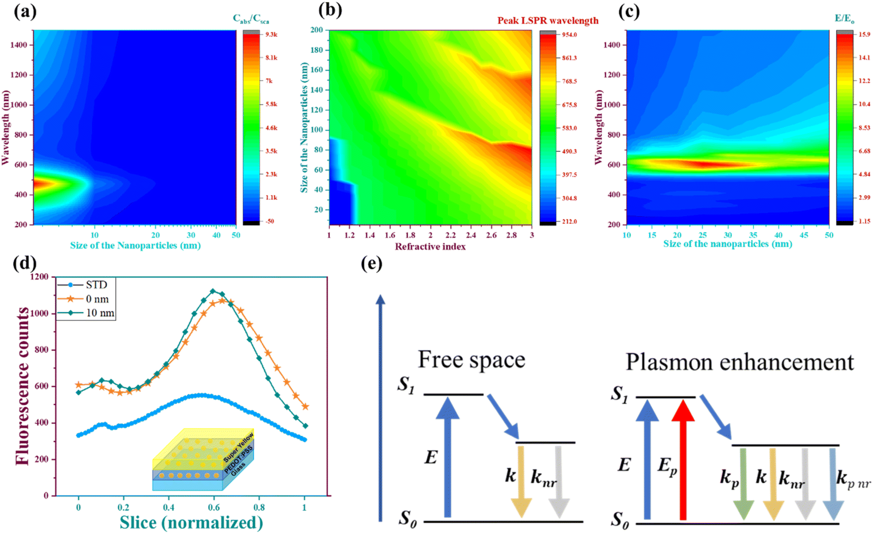 | ||
| Fig. 2 Light–plasmonic nanoparticle interaction and its effects on the nearby fluorophore. Calculated contour plots for spherical gold nanoparticles of different size, excited at different wavelengths in PEDOT:PSS surrounding medium: (a) ratio of absorption cross section to the scattering cross section; (b) dependence of the localised surface plasmon resonance on the size of the nanoparticles as well as on the refractive index of the surrounding medium; (c) local field enhancement compared to the incoming field from electromagnetic waves. (d) SHG-2PF 50 μm Z-stack at 1000 nm at 2.947 mW measurements exhibit a 2-fold increase in fluorescence intensity upon using PNPs. Inset, the architecture of the device used for the 2PF measurements. (e) Jablonski diagram representing various excitation and relaxation pathways for the fluorophores with and without PNPs. Where E = excitation, Ep = plasmon excitation rate. | ||
The fluorescence enhancement of the fluorophore (super yellow) upon incorporation into plasmonic Au-NPs is examined by a two-photon microscope, with an excitation wavelength of 1000 nm – the particular choice of excitation wavelength to excite both the nanoparticle and the super yellow66 and the second-harmonic of the laser wavelength, i.e. 500 nm – will interact with both nanoparticles and super yellow. In multi photon fluorescence (MPF), two or more photons are simultaneously absorbed to cause a higher energy electronic transition in a fluorescent molecule, in our case SY.
Three device architectures are studied by 2PF microscopy: glass/SY (STD), glass/AuNPs/SY and glass/AuNPs/PEDOT:PSS (10 nm)/SY. As can be seen in Fig. 2d, a 2-fold increment in the multi photon fluorescence (MPF) is observed upon incorporating the Au-NPs, compared to the standard sample (STD). We have to note here that Fig. 2d is not a spectrum, instead it is just the 2PF intensity (measured with a photomultiplier tube) as a function of slice depth. To understand if 15 nm gold nanoparticles are sufficiently large to show multi photon absorption, the logarithmic plot of the laser power versus emission intensity for the three different configurations is conducted and is shown in ESI Fig. 1.† Here all three configurations show slopes above 2, which represents the multi photon process.67 Since the study focuses on the influence of plasmons on fluorescence, henceforth in this article, the Au-NPs will be referred to as plasmonic nanoparticles (PNPs).
The observed 2-fold increment in the fluorescence can be explained as: both the PNPs and SY become excited upon exposure to the EM waves from the MPF laser, and the combined effects lead to the increase in MPF. But Fig. 2d shows only the incorporated PNPs induced and amplified by MPF in the SY. Therefore, the impact of the plasmons on the fluorescence mechanisms must be understood in detail.
The plasmon contribution to fluorescence could be elucidated considering the quantum yield. The relaxation rate for a fluorophore is denoted in terms of quantum yield, Q, given by eqn (2).53 With the plasmon modified fluorescence, the quantum yield becomes,68
| Qp = (k + kp)/(k + knr + kp + kp,nr) | (3) |
| Frad = kp/k | (4) |
| Fnon-rad = kp,nr/knr | (5) |
| Qp = Q(1 + Frad)/(1 + Fnon-rad + Q(Frad − Fnon-rad)) (ref. 69). | (6) |
Fig. 3a and b, represent a contour plot of Qp in comparison to Q. In Fig. 3a, Fnon-rad is plotted against intrinsic quantum yield by considering that Frad equals 10, and in Fig. 3b, Fnon-rad is plotted against Frad by considering the internal quantum efficiency of super yellow in a condensed phase. As is evident from Fig. 3a, there exist two distinct regions depending on the Fnon-rad compared to Frad. For Fnon-rad > Frad, plasmon enhanced quenching dominates, whereas for Fnon-rad < Frad, plasmon enhanced quantum yield overrides the quenching. However, it is also clear from Fig. 3a that, as Q approaches unity, the ability to improve Qp reduces even if Fnon-rad reduces to nil. The influence of Fnon-rad over Frad is also shown in Fig. 3b, for a given fluorophore, the plasmon enhanced quantum yield increases by increasing Frad in contrast to Fnon-rad. Therefore, an increase in the fluorescence intensity observed in Fig. 2d must be due to an enhancement in the radiative decay pathways compared to non-radiative decay pathways, hence plasmon enhanced fluorescence.
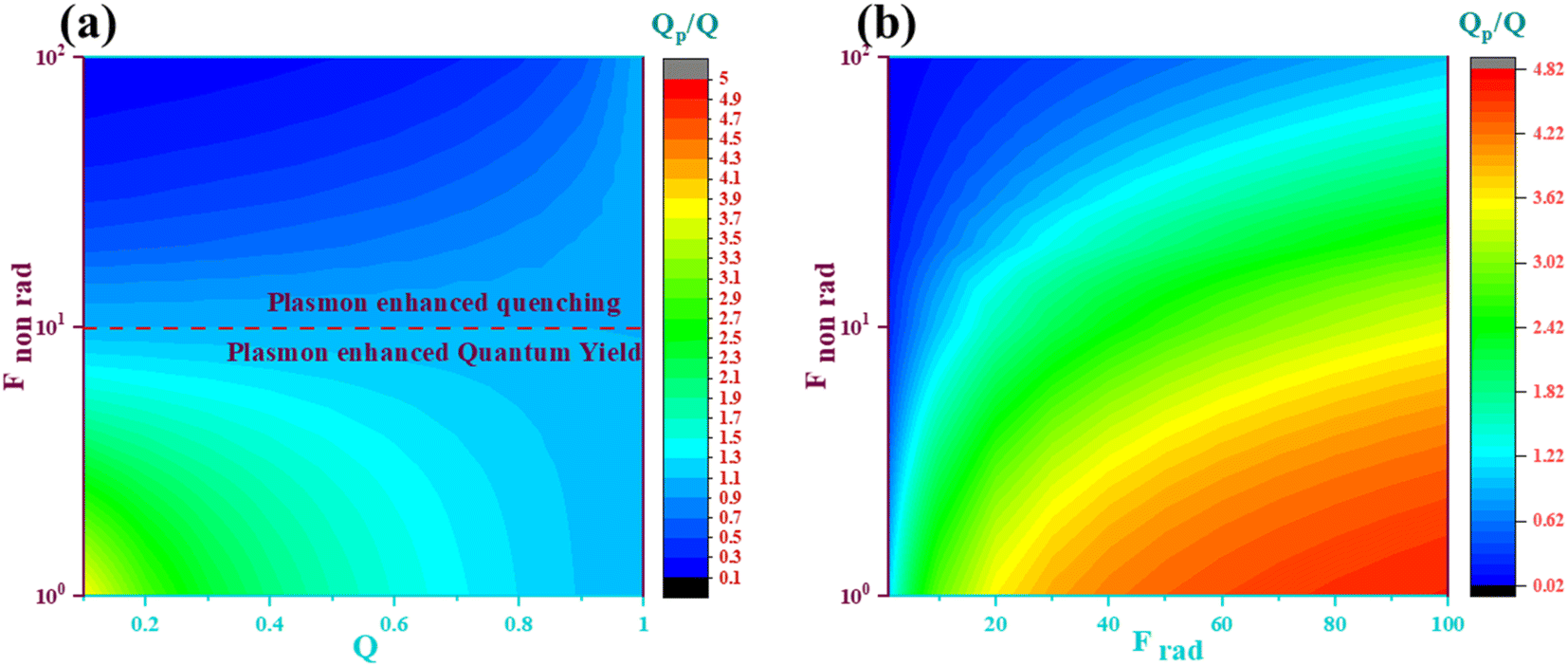 | ||
| Fig. 3 Plasmon enhanced quantum yield efficiency by: (a) keeping the plasmon enhanced radiative recombination constant at 10, with the plasmon enhanced non-radiative recombination and the intrinsic quantum yield of the fluorophore varied (Re simulated with permission from ref. 69, Copyright 2014, American Chemical Society); (b) keeping the intrinsic quantum yield of the fluorophore, in this case super yellow, constant at 20% and the plasmon enhanced radiative and non-radiative recombination is varied. | ||
The previous discussion is based on the PNPs being excited at their LSPR wavelength, and at LSPR conditions the contribution from both absorption and scattering is present. However, in the present case, the influence of the scattering is limited as the size of the PNPs used is 15 nm, therefore the contribution is more because of absorption, Fig. 2a. The increased absorption leads to enhanced electric near-field intensity around the PNPs. When the fluorophore is closer to the PNPs, an additional intensity of the electric field (plasma enhanced field intensity/E2/, induces local density of optical state) interacts with the fluorophore Em, and additional relaxation pathways are created, kp, kp,nr, (Fig. 2e). This allows the fluorophore to decay radiatively, or non-radiatively along with the initial relaxation pathways. At the optimized gap between the PNPs and fluorophore, the Fnon-rad becomes insignificant and Frad dominates, and enhanced fluorescence is seen, if not, the fluorophore experiences plasmon enhanced quenching. Therefore, the PNPs separated from SY by PEDOT:PSS should give enhanced fluorescence compared to other samples.
However, for both cases of incorporating the PNPs, almost the same behaviour is seen. This might be because the PEDOT:PSS spacer will induce an enhancement very locally, which is not observable with the microscope. Nevertheless, if the OLED architecture is designed well, by analysing the performance of the OLEDs it should be possible to conclude that the enhanced fluorescence is due to the reduction in non-radiative recombination. The plasmon enhancement in OLEDs could be understood as, upon electrical excitation, the electron–hole pair in the active layer, SY, would recombine and emit light at a certain wavelength, and if the designed nanoparticles have a localised surface plasmon resonance (LSPR) wavelength close to the emitted radiation wavelength, then the LSPR is activated. This LSPR then indeed increases the absorption and generates the field around the nanoparticle, which will later participate in altering non-radiative recombination pathways, kp,nr and also create a new radiative recombination pathway, km.
Fabrication of PNP incorporated OLEDs is shown in Fig. 1d, where PNPs are deposited using USSC. The surface coverage of the PNPs in an optoelectronic device is crucial because the field coupling between the closely spaced PNPs could induce an energy barrier to the mobility of the charges inside the device. Therefore, a COMSOL simulation is performed to investigate the same. The Au-NPs are placed in an envelope of PEDOT:PSS, with the illumination of light around 540 nm. Here the distance between the PNPs is varied and the influence of field coupling is simulated. It can be seen from Fig. 4a(i–iv), the closer the PNPs, the stronger the field coupling, and as the distance increases between the nanoparticles, the field coupling also reduces. The field coupling is almost negligible when the distance between the PNPs is around 3.5 times the diameter of the NPs. These results follow the Yamaguchi theory.66,70 Therefore, the surface coverage of the PNPs is kept around ∼2% to follow the Yamaguchi theory of field coupling and thereby enhance the charge transport properties in the OLEDs.
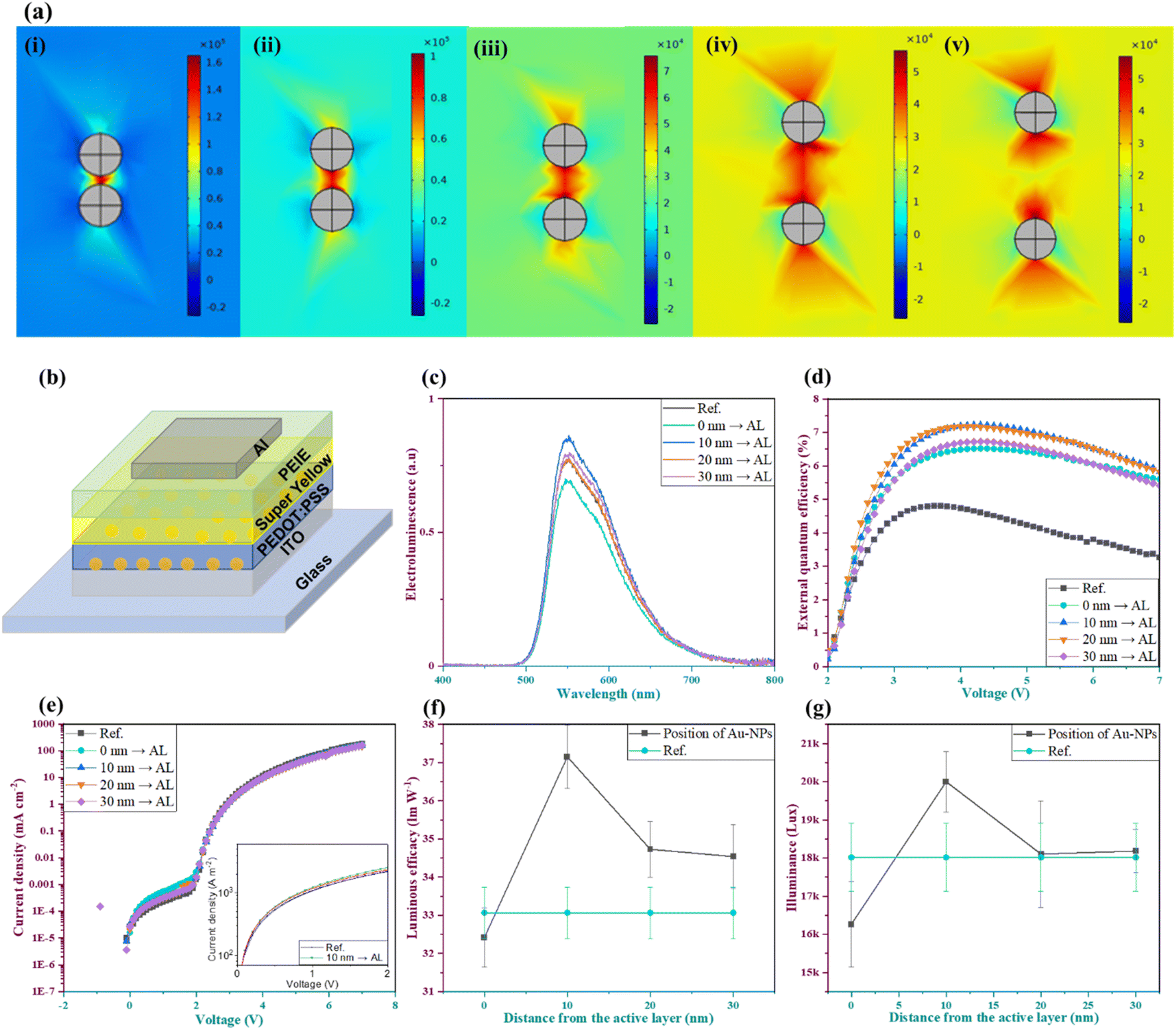 | ||
| Fig. 4 (a) Simulation on the PNPs enclosed in a PEDOT:PSS envelope by COMSOL multiphysics. The distance (D) between the Au-NPs is varied and the simulation clearly shows the influence of surface coverage on the field coupling: (i) D = 3 nm, (ii) D = 5 nm, (iii) D = 10 nm, (iv) D = 20 nm and (v) D = 30 nm. (b) Architecture of the OLEDs used in the present study. (c–g) Performance parameters for the PNPs incorporated OLEDs, wherein the position of the AL, SY and PNPs are varied: (c) electroluminescence curve, (d) external quantum efficiency, (e) current density vs. voltage, (f) luminous efficacy and (g) illuminance comparison. | ||
As elucidated in the previous section, upon incorporation of PNPs, the charge transport properties are altered in an organic semiconductor material, in our case, PNPs in PEDOT:PSS. Therefore a hole-only device consisting of ITO/PEDOT:PSS (with or without Au NPs)/MoO3/Ag (Fig. 4e inset) is fabricated to study the charge transport, and using space charge limited current at low voltage,71 hole mobilities are approximated.
 | (7) |
The hole mobilities were measured, upon incorporating the PNPs, and were found to be 7.7 × 10⁻⁵ cm2 V−1 s−1 whereas the reference sample possessed hole mobility of 1.3 × 10⁻⁵ cm2 V−1 s−1. This enhancement in the hole mobility is due to the isolated work function of gold nanoparticles around 5.1 eV,49,72 which promotes hole injection or transport onto the HOMO level of the PEDOT:PSS and the surface coverage of 2% did not influence the charge transport behaviour. Also, the stabilizer used for PNPs is PSS, which is a key ingredient in the PEDOT:PSS solution and hence does not restrict the mobility of holes. Buoyed by the fluorescence and hole mobility enhancement, the OLEDs are built for superior performance. The performance parameters – like electroluminescence, current density, external quantum efficiency, luminous efficacy and illuminance – are studied. The influence of PNPs and their vicinity to the fluorophore of the active layer is investigated by varying the space between them by varying the thickness of PEDOT:PSS. Five different sets of samples were built: (1) reference sample without the PNPs, (2) PNPs directly deposited on the active layer, (3) gap of 10 nm, (4) gap of 20 nm and (5) gap of 30 nm between the PNPs and fluorophore. Due to the layer-by-layer deposition of the PEDOT:PSS/gold nanoparticle/PEDOT:PSS, it is expected that the underlying layer is washed away due to the use of water as a solvent in PEDOT:PSS. To understand this, contact angle and atomic force microscopy measurements (AFM) were performed. The results are shown in ESI Fig. 2,† which shows that upon depositing gold nanoparticles on PEDOT:PSS, the water contact angle increases to 41° compared to the water contact angle of only PEDOT:PSS (15°). This shows that the gold nanoparticle decorated PEDOT:PSS layers are comparatively hydrophobic, which avoids the dissolution of the underlying PEDOT:PSS layer. The morphology and surface roughness (Ra) from the AFM images, shows that after the deposition of the first layer of PEDOT:PSS the Ra is 1.8 nm, and with gold nanoparticles deposited on top of the PEDOT:PSS the Ra is 2.1 nm, then finally the PEDOT:PSS on top of gold nanoparticles exhibits an Ra of 1.7 nm. There is no significant change in the Ra, indicating that there is no dissolution of any layers upon layer-by-layer deposition. Both the contact angle and AFM results confirm that there is no dissolution of the underneath deposited layer.
Among the five different sets of OLEDs, as expected for sample 2, the direct energy transfer from the fluorophore to the PNPs, via Förster energy transfer31 results in plasmon-enhanced quenching which results in reduced OLED performance, compared to other devices. The nanoparticles spaced 10 nm away from the active layer showcased superior performance compared to all the other devices, with an EQE of 7.22% and luminous efficacy of 37.15 lm W−1 compared with the reference samples EQE of 5.3% and luminous efficacy of 33.1 lm W−1 (Fig. 4d and f). This enhancement in the OLED performance parameters could be explained by considering the fluorescence intensity, current density, and illuminance measurements.
As seen from the 2PF measurements, the PNP devices showed enhanced fluorescence (Fig. 2d) but could not differentiate between the plasmon enhanced absorption and plasmon altered decay path for the fluorophores. Photoluminescence quantum yield measurements were performed to examine the contribution between the absorption and decay path, and the results are shown in ESI Fig. 3 .† However, due to the photobleaching upon irradiating with blue light, the distinction between the absorption and decay path could not be made. The absorbance and photoluminescence spectra depicted in ESI Fig. 3† show that there is no charge transfer between the nanoparticles and the fluorophore, and the incorporated Au-NPs are not acting as impurities. The absorption of the super yellow peaks around 443 nm hence will not lead to an increase in EQE. Therefore, an enhancement of nearly 40% EQE (Fig. 4d) could be due to: (1) far-field coupling and (2) near field coupling. As the size of the nanoparticles was 15 nm, the far-field coupling is suppressed, i.e., negligible contribution from the scattering. Therefore, the enhanced EQE indeed has to do with altering the decay channels, km and km,nr. A favourable condition for the near field coupling with the dipole of the fluorophore is achieved due to the plasmons, and it creates an additional radiative decay path, km. The near field coupling is also visible with devices where the distance between the fluorophore and the plasmonic nanoparticles is varied, as the gap between the fluorophore and PNPs increased further, the coupling between the near field and dipole of the fluorophore reduces and hence the OLED performance improves.
Also, the current density for all devices remains almost the same (Fig. 4e), i.e., the increased current is not responsible for the visible EL and illuminance enhancement (Fig. 4c and g). Therefore, a sweet spot of a 10 nm gap is required for the effective near field coupling of PNPs with the dipole of the fluorophore. Finally, a layer-by-layer deposition of PNPs, i.e. OLEDs with PNPs positioned simultaneously at 10 nm and 30 nm away from the active layer is built. The device architecture is shown in ESI Fig. 4.† However, there was no increase in either illuminance or efficacy of the OLEDs. One possible explanation could be due to the vertical closeness of the PNPs when deposited layer by layer which resulted in close pathways for the additional current to flow. This would increase the current density at low voltage as well as high voltage. From ESI Fig. 4,† it is evident that the injection at low voltage and high voltage is higher than the standard device. Therefore, this confirms the presence of the short channels created for the transport of charges by the randomly placed layer by layer PNPs. Finally, ESI Fig. 5 and 6† confirm that the plasmon enhanced light emission properties of the OLEDs are responsible for the observed enhancement in the light emission characteristics of the Au-NP incorporated devices, rather than the thickness of PEDOT:PSS and the alcohol treatment of the PEDOT:PSS.
Conclusions
In this work, 15 nm PSS stabilized Au-NPs were synthesised based on the calculated LSPR peaks and simulated near field enhancement which would be activated by the emission from the fluorophore. To enhance the hole mobilities inside an OLED, the surface coverage of the Au-NPs was optimized by the novel ultrasonic spray coating. The plasmon enhanced decay channels for the fluorophore in the presence of the optimized PNPs are investigated first by a 2PF microscope and later by the external quantum efficiency of the OLEDs. The observed 2-fold increment in the multi photon fluorescence intensity by the 2PF microscope combined with the obtained 40% increment in EQE for PNPs positioned 10 nm away from the fluorophore, exhibits an additional radiative decay path generated by the PNPs. Also, with the COMSOL simulation, it was seen that the surface coverage of the PNPs would induce field coupling between the PNPs, which later could alter the charge transport behaviour in organic semiconductors, therefore a surface coverage of ∼2% of PNPs deposited by USSC was optimized for, and used in, an OLED. The vertical position of 10 nm and surface coverage of ∼2% of PNPs exhibited the superior fluorescence, EQE, illuminance and luminous efficacy of the OLEDs. With this scheme of incorporating nanoparticles at an optimized position and surface coverage, achieved with the help of USSC, the performance of other fluorescent OLED systems can also easily be enhanced. The 10 nm gap between PNPs and the active layer resulted in a 33%, 20% and ∼40% increase in the electroluminescence, luminous efficacy and external quantum efficiency, respectively. Therefore, the simulation on the influence of the surrounding medium over the shift in LSPR peak wavelength of the Au-NPs as well as the field enhancement for different sizes of the nanoparticles, facilitates the selection of a particular nanoparticle for a specific light emission application. The plasmonic organic optoelectronic device scheme shown in this study shows for the first time the ease at which a 2PF microscope could investigate the PEF in an organic optoelectronic device without requiring tedious sample preparation. Also, the use of USSC for the first time to deposit the Au-NPs at will, and its control over the surface coverage, provides a new way of improving the performance of optoelectronic devices like solar cells, light emitting diodes and transistors, by incorporating PNPs with low-cost USSC technology.Data availability
The data that support the findings of this study are available from the corresponding authors, upon reasonable request.Author contributions
RSN, WD conceptualized the research work. ME synthesised the Au-NPs under the supervision of TV. VSN and SA performed the COMSOL simulation. YDC performed the 2PF measurements and analysed the 2PF results under the guidance of TV. MV performed PL measurements. RSN conducted the experiments, wrote the paper and analysed and validated the results under the supervision of WD. WD acquired the funding for the research work. All the authors contributed in review and editing.Conflicts of interest
The authors declare no conflict of interest.Acknowledgements
The authors would like to thank the BOF fund of UHasselt for funding the present work and would also like to thank Naveen Reddy for the discussion on the deagglomeration of Au-NPs. The authors would also like to thank NMIT for allowing us to utilize the COMSOL to simulate the Au-NPs.References
- K. H. Drexhage, J. Lumin., 1970, 1–2, 693 CrossRef
.
- W. L. Barnes, J. Mod. Opt., 1998, 45, 661 CrossRef CAS
- F. Tam, G. P. Goodrich, B. R. Johnson and N. J. Halas, Nano Lett., 2007, 7, 496 CrossRef CAS PubMed
- P. Taylor and W. L. Barnes, J. Mod. Opt., 1998, 45, 661 CrossRef
- R. R. Chance, A. H. Miller, A. Prock and R. Silbey, J. Chem. Phys., 1975, 63, 1589 CrossRef CAS
- S. Weiss, Science, 1999, 283, 1676 CrossRef CAS PubMed
- J. R. Lakowicz, Anal. Biochem., 2001, 298, 1 CrossRef CAS PubMed
- V. Giannini, A. I. Fernández-Domínguez, S. C. Heck and S. A. Maier, Chem. Rev., 2011, 111, 3888 CrossRef CAS PubMed
- F. Liu and J. M. Nunzi, Org. Electron., 2012, 13, 1623 CrossRef CAS
- K. Mosshammer, M. Sudzius, S. Meister, H. Fröb, A. M. Steiner, A. Fery and K. Leo, Appl. Phys. Lett., 2021, 118, 013301 CrossRef CAS
- C. Chen, C. A. Bobisch and W. Ho, Science, 2009, 325, 981 CrossRef CAS PubMed
- J. R. Lakowicz, Anal. Biochem., 2001, 298, 1 CrossRef CAS PubMed
- S. Khatua, P. M. R. Paulo, H. Yuan, A. Gupta, P. Zijlstra and M. Orrit, ACS Nano, 2014, 8, 4440 CrossRef CAS PubMed
- J. R. Lakowicz, Anal. Biochem., 2005, 337, 171 CrossRef CAS PubMed
- P. Bharadwaj, P. Anger and L. Novotny, Nanotechnology, 2007, 18, 044017 CrossRef
- H. Mertens, A. F. Koenderink and A. Polman, Phys. Rev. B: Condens. Matter Mater. Phys., 2007, 76, 1 CrossRef
- M. A. Alkhalayfeh, A. A. Aziz and M. Z. Pakhuruddin, Renewable Sustainable Energy Rev., 2021, 141, 110726 CrossRef CAS
- D. D. Zhang, J. L. Xu and H. B. Sun, Adv. Opt. Mater., 2021, 9, 1 Search PubMed
- M.-K. Chuang, C.-H. Lin and F.-C. Chen, Dyes Pigm., 2020, 180, 108412 CrossRef CAS
- A. Y. Gladkikh, M. I. Kozlov, A. A. Vashchenko, A. V. Medved’ko, A. S. Goloveshkin, A. V. Bolshakova, E. V. Latipov and V. V. Utochnikova, Dalton Trans., 2022, 51, 16065 RSC
- B. Liu, M. Januar, J.-C. Cheng, K. Hatanaka, H. Misawa and K.-C. Liu, Nanoscale, 2021, 13, 12164 RSC
- A. M. El-Mahalawy and A. R. Wassel, Opt. Laser Technol., 2020, 131, 106395 CrossRef CAS
- J. Linnet, A. R. Walther, O. Albrektsen, L. Tavares, R. L. Eriksen, P. B. W. Jensen, A. Osadnik, S. Hassing, A. Lützen and J. Kjelstrup-Hansen, Org. Electron., 2017, 46, 270 CrossRef CAS
- R. Zakaria, W. K. Lin and C. C. Lim, Appl. Phys. Express, 2012, 5, 082002 CrossRef
- S. A. Choulis, M. K. Mathai and V. E. Choong, Appl. Phys. Lett., 2006, 88, 86 Search PubMed
- J. H. Park, Y. T. Lim, O. O. Park, J. K. Kim, J. W. Yu and Y. C. Kim, Chem. Mater., 2004, 16, 688 CrossRef CAS
- T. Kim, H. Kang, S. Jeong, D. J. Kang, C. Lee, C. H. Lee, M. K. Seo, J. Y. Lee and B. J. Kim, ACS Appl. Mater. Interfaces, 2014, 6, 16956 CrossRef CAS PubMed
- D. H. Kim and T. W. Kim, Opt. Express, 2015, 23, 11211 CrossRef CAS PubMed
- S. H. Kim, T. S. Bae, W. Heo, T. Joo, K. D. Song, H. G. Park and S. Y. Ryu, ACS Appl. Mater. Interfaces, 2015, 7, 15031 CrossRef CAS PubMed
- Y. Xu, H. Zhou, R. Zhang, Y. Liu, Q. Zhang, S. Zhang, L. Zhang, S. Chen, L. Deng, Y. Qian, L. Wang and W. Huang, AIP Adv., 2015, 5, 067121 CrossRef
- B. Munkhbat, H. Pöhl, P. Denk, T. A. Klar, M. C. Scharber and C. Hrelescu, Adv. Opt. Mater., 2016, 4, 772 CrossRef CAS
- J. Zhu, X. Li, W. Zheng, B. Wang and Y. Tian, Nanotechnology, 2018, 29, 055701 CrossRef PubMed
- A. Fujiki, T. Uemura, N. Zettsu, M. Akai-Kasaya, A. Saito and Y. Kuwahara, Appl. Phys. Lett., 2010, 96, 043307 CrossRef
- T. Tanaka, Y. Totoki, A. Fujiki, N. Zettsu, Y. Miyake, M. Akai-Kasaya, A. Saito, T. Ogawa and Y. Kuwahara, Appl. Phys. Express, 2011, 4, 032105 CrossRef
- Y. Xiao, J. P. Yang, P. P. Cheng, J. J. Zhu, Z. Q. Xu, Y. H. Deng, S. T. Lee, Y. Q. Li and J. X. Tang, Appl. Phys. Lett., 2012, 100, 013308 CrossRef
-
L. Bo, K. C. Liu, H. Q. Xiao, C. H. Wu and C. S. Lai, 2012 Photonics Glob. Conf. PGC, 2012, vol. 2012, p. 333 Search PubMed
- S. J. Ko, H. Choi, W. Lee, T. Kim, B. R. Lee, J. W. Jung, J. R. Jeong, M. H. Song, J. C. Lee, H. Y. Woo and J. Y. Kim, Energy Environ. Sci., 2013, 6, 1949 RSC
- D. Wang, K. Yasui, M. Ozawa, K. Odoi, S. Shimamura and K. Fujita, Appl. Phys. Lett., 2013, 102, 9 Search PubMed
- H. Sung, J. Lee, K. Han, J. K. Lee, J. Sung, D. Kim, M. Choi and C. Kim, Org. Electron., 2014, 15, 491 CrossRef CAS
- P. J. Jesuraj and K. Jeganathan, RSC Adv., 2015, 5, 684 RSC
- Y. Zhuang, L. Liu, X. Wu, Y. Tian, X. Zhou, S. Xu, Z. Xie and Y. Ma, Part. Part. Syst. Charact., 2019, 36, 1800077 CrossRef
- P. J. Jesuraj and K. Jeganathan, RSC Adv., 2015, 5, 684 RSC
- B. Xiao, G. N. Rutherford, A. P. Sharma, S. K. Pradhan, C. E. Bonner and M. J. Bahoura, Sci. Rep., 2020, 10, 1 CrossRef PubMed
- P. J. Jesuraj, K. Jeganathan, M. Navaneethan and Y. Hayakawa, Synth. Met., 2016, 211, 155 CrossRef CAS
- L. Lin, Q. Zhang, X. Li, M. Qiu, X. Jiang, W. Jin, H. Gu, D. Y. Lei and J. Ye, ACS Nano, 2018, 12, 6492 CrossRef CAS PubMed
- D.-H. Lan, S.-H. Hong, L.-H. Chou, X.-F. Wang and C.-L. Liu, J. Power Sources, 2018, 390, 270 CrossRef CAS
- K. X. Steirer, M. O. Reese, B. L. Rupert, N. Kopidakis, D. C. Olson, R. T. Collins and D. S. Ginley, Sol. Energy Mater. Sol. Cells, 2009, 93, 447 CrossRef CAS
- H. Huang, J. Shi, L. Zhu, D. Li, Y. Luo and Q. Meng, Nano Energy, 2016, 27, 352 CrossRef CAS
- L. Zhou and M. R. Zachariah, Chem. Phys. Lett., 2012, 525–526, 77 CrossRef CAS
- I. Verboven, R. S. Nithyanandakumar, M. Van Landeghem, H. Pellaers, B. Ruttens, J. D’Haen, K. Vandewal and W. Deferme, Nano Sel., 2021, 1, 851–863 Search PubMed
- C. Jeong, H. Ko, H.-T. Kim, K. Sun, T.-H. Kwon, H. E. Jeong and Y.-B. Park, ACS Appl. Mater. Interfaces, 2020, 12, 18813 CrossRef CAS PubMed
- J.-L. Wu, F.-C. Chen, Y.-S. Hsiao, F.-C. Chien, P. Chen, C.-H. Kuo, M. H. Huang and C.-S. Hsu, ACS Nano, 2011, 5, 959 CrossRef CAS PubMed
- J. F. Li, C. Y. Li and R. F. Aroca, Chem. Soc. Rev., 2017, 46, 3962 RSC
- Y. Fu, J. Zhang and J. R. Lakowicz, J. Am. Chem. Soc., 2010, 132, 5540 CrossRef CAS PubMed
- E. M. van Schrojenstein Lantman, T. Deckert-Gaudig, A. J. G. Mank, V. Deckert and B. M. Weckhuysen, Nat. Nanotechnol., 2012, 7, 583 CrossRef CAS PubMed
- M. Ramírez-Maureira, C. Victor Vargas, A. Riveros, P. J. G. Goulet and I. O. Osorio-Román, Mater. Chem. Phys., 2015, 151, 351 CrossRef
- C.-Y. Li, J.-C. Dong, X. Jin, S. Chen, R. Panneerselvam, A. V. Rudnev, Z.-L. Yang, J.-F. Li, T. Wandlowski and Z.-Q. Tian, J. Am. Chem. Soc., 2015, 137, 7648 CrossRef CAS PubMed
- A. Hartschuh, Angew. Chem., Int. Ed., 2008, 47, 8178 CrossRef CAS PubMed
- J. Olesiak-Banska, M. Waszkielewicz, P. Obstarczyk and M. Samoc, Chem. Soc. Rev., 2019, 48, 4087 RSC
- E. Palacios-Lidon, E. Escasain, E. Lopez-Elvira, A. M. Baro and J. Colchero, Sol. Energy Mater. Sol. Cells, 2013, 117, 15 CrossRef CAS
- J. Turkevich, P. C. Stevenson and J. Hillier, Discuss. Faraday Soc., 1951, 11, 55 RSC
- F. P. C. Lauterbur, Nature, Phys. Sci., 1973, 241, 20 CrossRef
- J. Kimling, M. Maier, B. Okenve, V. Kotaidis, H. Ballot and A. Plech, J. Phys. Chem. B, 2006, 110, 15700 CrossRef CAS PubMed
- Gold Nanoparticles: Properties and Applications|Sigma-Aldrich, can be found under https://www.sigmaaldrich.com/technical-documents/articles/materials-science/nanomaterials/gold-nanoparticles.html, n.d.
-
S. J. Oldenburg, Light scattering from gold nanoshells, Rice Univ., Houston, TX, USA, 2000, p. 98 Search PubMed
-
M. A. van der Veen, D. E. De Vos and T. Verbiest, Phys. Chem. Interfaces Nanomater. IX, 2010, vol. 7758, p. 77580D Search PubMed
- R. A. Farrer, F. L. Butterfiefd, V. W. Chen and J. T. Fourkas, Nano Lett., 2005, 5, 1139 CrossRef CAS PubMed
- M. Bauch, K. Toma, M. Toma, Q. Zhang and J. Dostalek, Plasmonics, 2014, 9, 781 CrossRef CAS PubMed
- P. Upconversion, D. M. Wu, A. Garc, A. Salleo, J. A. Dionne, 2014.
- T. Yamaguchi, S. Yoshida and A. Kinbara, Thin Solid Films, 1974, 21, 173 CrossRef CAS
- S. L. M. Van Mensfoort and R. Coehoorn, Phys. Rev. B: Condens. Matter Mater. Phys., 2008, 78, 1 Search PubMed
- D. M. Wood, Phys. Rev. Lett., 1981, 46, 749 CrossRef CAS
Footnote |
| † Electronic supplementary information (ESI) available. See DOI: https://doi.org/10.1039/d2na00753c |
| This journal is © The Royal Society of Chemistry 2023 |