
Unraveling the infrared detection properties of Bi2Te3 depending on thickness under the semiconductor and metal surface states†
Qijun
Kao‡
 a,
Yongfeng
Jia‡
d,
Zhihao
Wu
a,
Zhangxinyu
Zhou
a,
Xun
Ge
b,
Jian
Peng
a,
Piotr
Martyniuk
e,
Jin
Wang
*bc,
Chuanbin
Wang
*a and
Fang
Wang
*b
a,
Yongfeng
Jia‡
d,
Zhihao
Wu
a,
Zhangxinyu
Zhou
a,
Xun
Ge
b,
Jian
Peng
a,
Piotr
Martyniuk
e,
Jin
Wang
*bc,
Chuanbin
Wang
*a and
Fang
Wang
*b
aState Key Lab of Advanced Technology for Materials Synthesis and Processing, Wuhan University of Technology, Wuhan 430070, China. E-mail: wangcb@whut.edu.cn
bShanghai Institute of Technical Physics, Chinese Academy of Science, Shanghai 200080, China. E-mail: wang_jin_1988@163.com; fwang@mail.sitp.ac.cn
cMOE Key Laboratory of Advanced Micro-Structure Materials, Shanghai Frontiers Science Center of Digital Optics, Institute of Precision Optical Engineering, and School of Physics Science and Engineer, Tongji University, Shanghai 200092, China
dSchool of Materials and Chemistry, Southwest University of Science and Technology, Mianyang 621010, China
eInstitute of Applied Physics, Military University of Technology, 2 Kaliskiego St., 00-908 Warsaw, Poland
First published on 1st February 2025
Abstract
Bi2Te3 recently emerges as a promising candidate material for the next generation of mid-wave to long-wave infrared photodetection owing to its exceptionally narrow bandgap (approximately 0.2 eV) and the favorable photoelectronic properties. In particular, its topological insulator structure is safeguarded by time-reversal symmetry, leading to electronic structures with distinct surface and bulk states as well as distinctive optoelectronic properties. This study examines the infrared detection mechanism of Bi2Te3 across various thicknesses, aiming to elucidate the transport behavior and characteristics of internal carriers in Bi2Te3 under the complex interplay between the bulk state and surface states. Bi2Te3 films at various thicknesses were synthesized pulsed laser deposition with varied number of pulses which determines the actual thickness. The bandgap and the photoelectric response mechanism of Bi2Te3 at different layer thicknesses were investigated, and the charge carrier transport dynamics across layers were clarified. To summarize, this study offers a theoretical basis for advancing photoelectric detection devices designed to regulate Bi2Te3 at distinct thicknesses.
 Fang Wang | Fang Wang received her Ph.D. degree in Science from East China Normal University, Shanghai, China, in 2019. She is currently an associate professor in Shanghai Institute of Technical Physics, Chinese Academy of Sciences. Her research interests focus on mechanism and application of infrared photodetectors. She received the National Science Fund for Excellent Young Scholars in 2024 and CAS Pioneer Hundred Talents Program in 2022 and Shanghai Sailing Program in 2020. She was a Highly Cited Researcher (Clarivate) in 2024. She has authored or coauthored more than 60 technical journal papers including in Nature Materials, Nature Electronics, Nature Communications, Science Advances. |
1. Introduction
For more than half a century, Bi2Te3 has been valued for its stability at room temperature and its high thermoelectric performance coefficient,1–3 making it a widely used material in thermoelectric applications. Recently, Bi2Te3, which is recognized as a 3D topological insulator, has been predicted to possess a bulk bandgap together with gapless surface states characterized by a single Dirac cone, which triggers many intriguing physical properties.4,5 This creates opportunities for the development of advanced optoelectronic devices, particularly broad-spectrum infrared detectors.6 To achieve optimal infrared detection performance, two conditions must be met: 1. The material must possess a sufficiently narrow bandgap.7–9 When exposed to external light, electrons within the material can undergo a transition from the valence band to the conduction band or from a lower to a higher energy level under weak infrared light. 2. High carrier mobility is required.10–14 Excited electrons can be rapidly transported, allowing for the effective separation of electrons and holes. Otherwise, electrons will be captured by holes, resulting in a transition from a high to a low energy level. The bulk bandgap of Bi2Te3 is approximately 0.2 eV.15 As described by the formula λe = 1.24/Eg, the calculated cutoff wavelength is 6.8 μm, which allows for mid-wave to long-wave infrared photodetection and enables a broad spectral range.16–18 Moreover, Dirac surface states, protected by time-reversal symmetry, help suppress the backscattering of electrons. The topological protection mechanism enables the device to exhibit outstanding chemical stability while maintaining rapid carrier transport and long-term operational stability.19–21 The unique interlayer structure eliminates surface dangling bonds,22 which helps reduce carrier generation–recombination noise.It is precisely owing to the layered structure of Bi2Te3 that quantum effects arising from changes in its thickness influence its fundamental properties. Rogacheva et al.23 fabricated and investigated the thickness-dependent quantum oscillations of the transport properties of Bi2Te3 thin films using pulsed laser deposition. A subsequent study24 investigated the relationship between the transport properties of gapless surface states and film thickness, confirming that two-dimensional transport through topological surface states dominates the conductance of films as thin as 10 nm. It has been confirmed that ultra-thin films are an effective means of suppressing the contribution of bulk states to transport. Using a simple hot-pressing strategy, Hussain et al.25 regulated the visible light surface plasmon resonance mode and intensity of Bi2Te3 through thickness adjustment. Particularly as an emerging material for infrared detection, Zhang et al.26 fabricated optothermal ferroelectric field-effect transistors (FeFETs) by growing Bi2Te3 thin films on PMN-PT (111) substrates. The devices exhibited multiple responses to light and electric fields at room temperature using ferroelectric and thermoelectric effects. Wali et al.27 used physical vapor deposition to develop high-quality rubrene (C42H28)/topological insulator (Bi2Te3) organic–inorganic heterostructures. In the near-infrared region, the device exhibited a photoresponsivity of 852.7 A W−1, a detectivity of 1.42 × 10¹³ Jones, and an ultrafast response time (τrise = 14 μs and τdecay = 16.2 μs). Kim et al.28 developed optoelectronic neuromorphic transistors with Bi2Te3 as the absorption layer and successfully broadened the absorption spectrum. The device achieved neuromorphic properties. However, there has been a lack of in-depth studies on the thickness dependence of the infrared detectability of Bi2Te3 thin films.
In this study, ultrathin Bi2Te3 films were prepared using Pulsed laser deposition (PLD), with the film thickness precisely controlled by varying the number of laser pulses. We focused on the photoelectric mechanism and electron transport process of Bi2Te3 at different thicknesses which are significant for advancing Bi2Te3 applications in photoelectric devices.
2. Experimental
2.1 Synthesis of Bi2Te3
Bi2Te3 films were fabricated on SiO2 (285 nm)/Si substrates using a PLD, with laser pulse numbers ranging from 120 to 480. The Bi2Te3 target had a Te/Bi atomic ratio of 3![[thin space (1/6-em)]](https://www.rsc.org/images/entities/char_2009.gif) :2 and was composed of high-purity Te (99.9%) and Bi (99.9%) elements, which was ablated by a KrF-excimer laser (248 nm wavelength, 20 ns pulse length) with a laser energy of 50 mJ and a frequency of 2 Hz. The laser energy density was 4.25 J cm−2. To prevent the oxidation of the Bi2Te3 films, the vacuum chamber was evacuated to 1 × 10⁻⁵ Pa before deposition. A pre-deposition step was conducted to clean the target surface. The substrate temperature was maintained at 250 °C during the deposition, with a chamber pressure below 1.3 × 10⁻⁵ Pa. The target-to-substrate distance was set at a constant 10 cm, and the target and substrate rotations were activated to ensure a uniform film deposition across the substrate.
:2 and was composed of high-purity Te (99.9%) and Bi (99.9%) elements, which was ablated by a KrF-excimer laser (248 nm wavelength, 20 ns pulse length) with a laser energy of 50 mJ and a frequency of 2 Hz. The laser energy density was 4.25 J cm−2. To prevent the oxidation of the Bi2Te3 films, the vacuum chamber was evacuated to 1 × 10⁻⁵ Pa before deposition. A pre-deposition step was conducted to clean the target surface. The substrate temperature was maintained at 250 °C during the deposition, with a chamber pressure below 1.3 × 10⁻⁵ Pa. The target-to-substrate distance was set at a constant 10 cm, and the target and substrate rotations were activated to ensure a uniform film deposition across the substrate.
2.2 Characterization
The phase and composition of the Bi2Te3 thin films were analyzed using X-ray diffraction (XRD, DMAX 1400, Japan) over a 2θ range of 5–60° at a scanning speed of 10° min−1. The Cu Kα line (λ = 0.154 nm) was used as the radiation source. The Raman spectrum (Horiba Xplora Plus, Japan) was used to analyze internal molecular vibrations and intermolecular forces, with an argon ion laser as the excitation source at a wavelength of 532 nm. High-resolution transmission electron microscopy (HRTEM) was employed to investigate the crystalline structure, thickness, and layering of Bi2Te3. TEM samples were prepared using a focused ion-beam system.2.3 Device fabrications and measurements
A Ti/Pt (10 nm/80 nm) layer was deposited on the surface of the Bi2Te3 film as the electrode using electron beam evaporation. Contacts were deposited over the sample using a shadow mask. The electrical properties of the films were measured using a probe station (CRX-6.5 K, Lake Shore) equipped with a Keithley electrometer (6517B). A 1064 nm wavelength laser served as the excitation source for assessing the device's photoresponse. For low-temperature testing at 7 K, the work pressure was maintained below 5.0 × 10⁻³ Pa.2.4 Calculation
The first-principles calculations were carried out using the VASP software package based on density functional theory. The exchange–correlation functional employed the Perdew–Burke–Ernzerhof (PBE) functional within the generalized gradient approximation (GGA), and the interaction between electrons and ions was modeled using the Projected Augmented Wave method. When optimizing the structure of Bi2Te3, the convergence criteria of the system energy and force were set to 10−5 eV and 10−2 eV Å−1, respectively, and the plane wave cutoff energy was 300 eV. Considering the van der Waals force between the layers of Bi2Te3, the DFT-D3 functional was employed to model the interlayer interaction and determine the interlayer spacing. For a few-layer Bi2Te3, to prevent interactions between mirror images, a vacuum layer with a thickness of 15 Å was introduced. The k-point sampling in the Brillouin zone employed the Monkhorst–Pack method centered on the gamma point. During the optimization of the Bi2Te3 structure, a k-point grid of 9 × 9 × 1 was chosen.3. Results and discussion
In our study, atomic layers thick Bi2Te3 films were fabricated by the PLD method. Bi2Te3 has a rhombohedral crystal structure with the space group D3d5-R (-3)m, which has five atoms in one-unit cell. As illustrated in Fig. 1(a), the atomic arrangement can be visualized as a layered sandwich structure. This structure is composed of five monatomic sheets, referred to as quintuple layers (QLs), stacked within each sandwich layer. The sequence of QLs along the c axis is –[Te(1)–Bi–Te(2)–Bi–Te(1)]–, which has a thickness of ∼1 nm.29 Here, subscripts (1) and (2) denote two distinct coordination environments for the anions in the crystal structure. The binding between adjacent QLs primarily arises from weak van der Waals forces, whereas bonding within each QL is either covalent or partially ionic, resulting in a preferential cleavage plane between adjacent QLs.30 The two images on the right display the top and side views along the c-axis, providing a clear representation of the quintuple-layer structure.31 Photographs of the as-fabricated Bi2Te3 films with varying numbers of laser pulses are shown in the inset of Fig. 1(b). It is evident that the color of the Bi2Te3 films changes as the number of laser pulses increases, transitioning from blue to purple and then to white, a phenomenon primarily attributed to thin-film interference.32 The crystal structure of the synthesized Bi2Te3 thin films was evaluated by XRD analysis. Fig. 1(b) presents the representative test results for Bi2Te3 films prepared with varying pulse numbers, showing diffraction peaks at 2θ angles of 8.6°, 17.7°, and 44.7°. The diffraction peaks at these angles correspond to the (003), (006), and (0015) planes of Bi2Te3, respectively. In general, the (00l) diffraction peaks (l = 3, 6, and 15) are indicative of the three-layer stacking sequence within the five-layer structure of Bi2Te3,33 aligning with the crystal structure presented in Fig. 1(a).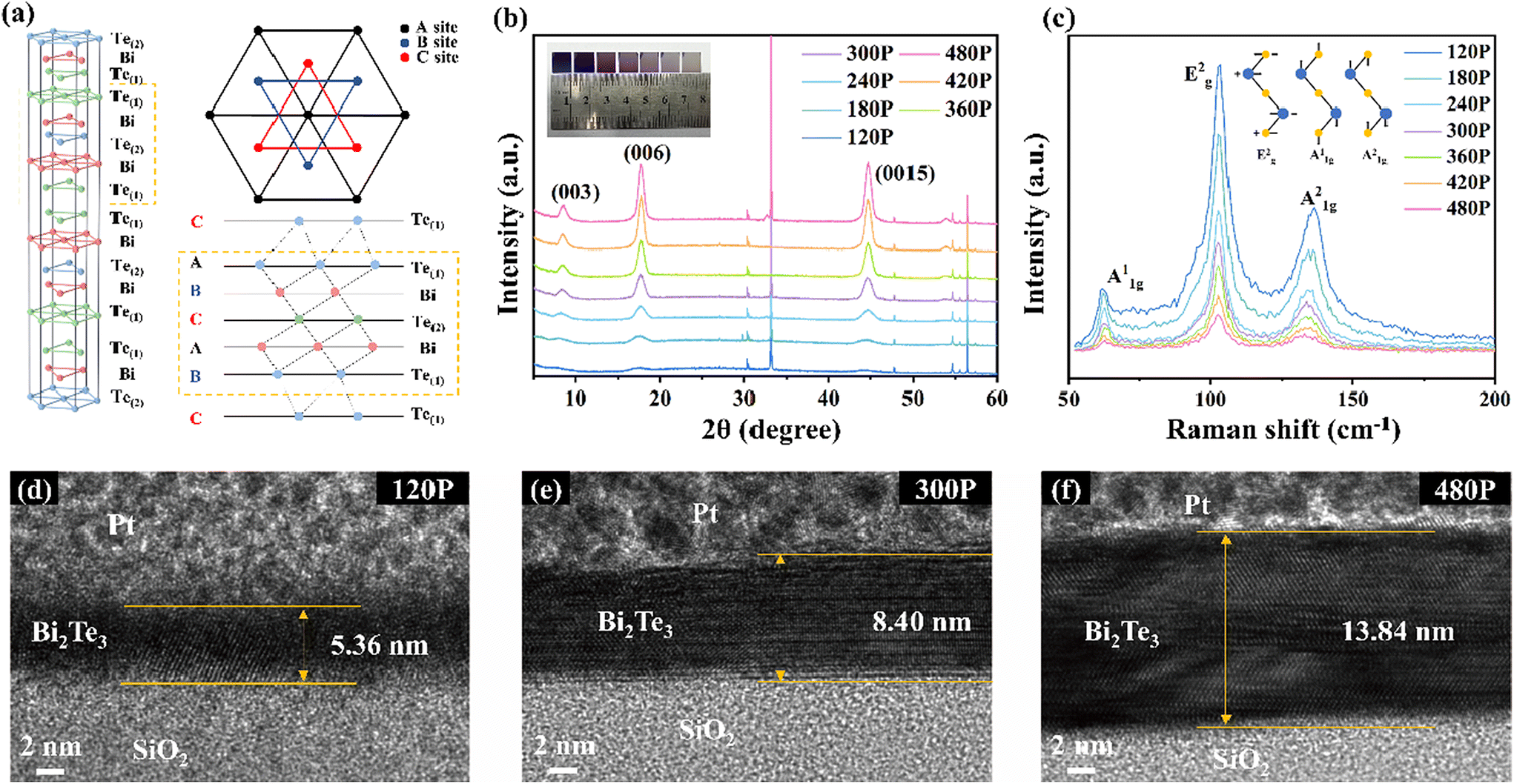 | ||
| Fig. 1 Crystal structure and characterization of Bi2Te3 thin films prepared via PLD. (a) Schematic of the Bi2Te3 quintuple crystal structure (left). A top view along the c-axis shows that the triangular lattice within a quintuple layer contains three distinct positions, labeled A, B, and C (top right). A side view of the quintuple layer structure reveals that along the c-axis, the stacking sequence of Te and Bi atomic layers is denoted as Te(1)–Bi–Te(2)–Bi–Te(1) (bottom right). (b) Raman patterns of Bi2Te3 thin films with different pulse numbers (the inset shows a photograph of the Bi2Te3 thin film). (c) Raman spectrum of Bi2Te3 thin films with different pulse numbers (the inset shows a schematic of the main lattice vibrations in the quintuple structure). (d–f) Cross-sectional high-resolution TEM images of Bi2Te3 thin films with pulse numbers of 120, 300, and 480 (SiO2 at the bottom and Pt at the top). | ||
Raman spectroscopy is a widely utilized non-destructive technique for analyzing interactions between phonons and electrons in materials.34,35 This method is particularly valuable for studying two-dimensional materials with varying numbers of stacking layers. The Raman spectrum of the prepared Bi2Te3 films has been systematically analyzed. As shown in Fig. 1(c), the measured Raman spectrum reveals three prominent peaks – A11g, E2g, and A21g – appearing at 61, 103, and 133 cm−1, respectively. The inset of Fig. 1(c) shows a schematic diagram of the lattice vibrations in the QL, where “E” denotes vibrations along the in-plane (ab plane) direction and “A” indicates out-of-plane (c axis) vibrations. The symbols “+” and “−” represent atomic movements in the plane toward and away from the observer, respectively. In the A11g mode, the outer Te–Bi pairs move in phase, whereas in the E2g and A21g modes, the outer Te–Bi pairs move in opposite phases.36Fig. 1(c) demonstrates a clear red shift in the frequency position of the A21g mode as the layer number increases.37 This shift is primarily attributed to phonon confinement effects arising from the reduced number of Bi2Te3 layers, leading to phonon mode hardening. The hardening of the mode is influenced by interlayer van der Waals interactions, which increase the restoring forces on the out-of-plane atoms and thereby impact the frequency of the A21g mode. In addition, the thinner Bi2Te3 samples exhibit stronger Raman signals, while thicker samples show weaker signals.36,37 The Raman peak intensity generally increases as the film thickness decreases, thereby enhancing light interaction with the material, a phenomenon primarily attributed to light attenuation.
Owing to their atomic-scale thickness and quantum confinement effects, 2D materials exhibit high sensitivity to metal–semiconductor interfaces (electrodes), which can substantially influence or degrade their quality. The achievement of high-quality 2D materials necessitates clean, well-defined interfaces. Transmission electron microscopy (TEM), offering atomic-level resolution, serves as a powerful tool for examining crystal structures and is extensively employed to assess the interface quality of 2D materials.38,39 To further investigate the microstructure of the Bi2Te3 films, TEM was used to observe the cross-sectional morphology of the films. Fig. 1(d) showed that the sample subjected to 120 laser pulses has a thickness of approximately 5.36 nm. As the number of pulses increases to 300 and 480, as shown in Fig. 1(e and f), the film thickness increases to 8.4 and 13.84 nm, respectively. The three cross-sectional images illustrated the thickness dependence of the films, confirming that Bi2Te3 grows layer by layer through PLD. In these two samples, the contrast between the light and dark areas in the image distinctly reveals the interlayer spacing of Bi2Te3, emphasizing its characteristic layered structure.
The resistance of the Bi2Te3 films was measured over a temperature range of 7–300 K (the vertical axis is presented in logarithmic scale), revealing different trends in resistance variation with temperature. As shown in Fig. 2(a), the initial resistance of the two thinnest samples measured tens of thousands of ohms at low temperatures, which gradually decreased as the temperature rose. At low temperatures, few electrons possess sufficient energy to transition from the valence band to the conduction band, thereby limiting the number of free carriers available for conduction. As the temperature increases, thermal energy excites more electrons to undergo this transition. This process generates additional free electrons in the conduction band and corresponding holes in the valence band, thereby increasing the carrier concentration and reducing film resistance. The trend observed in the sample depicted in the middle of Fig. 2(a) aligns with that of the previous two samples, although the variation is less pronounced. The aforementioned films exhibited semiconducting behavior. As the number of layers increases, the resistance of the films also rises with temperature, suggesting metallic behavior. This effect is primarily attributed to the intensification of phonon scattering at higher temperatures, which results in more frequent interactions between carriers and phonons. As a result, the carrier mobility decreases, leading to an increase in resistance. As the number of film layers decreases, the resistance at the same temperature gradually increases. This effect is primarily attributed to the reduced thickness of the thin film, where significant overlap occurs between wave functions on its upper and lower surfaces. The hybridization between these surfaces opens gaps in the surface states. As a result, the metallic surface states are effectively suppressed, contributing to an increase in resistance.8,40,41 The optoelectronic performance of the device was measured, as illustrated in Fig. 2(b–d). The differences in the photoresponse of the films exhibiting distinct behaviors were examined using the I–V curves. The responsivity (R) and detectivity (D*) were calculated based on the data in the Fig. 2(b). Fig. S1† demonstrates that the R and D* of the sample gradually decrease as the light intensity increases.
 | ||
| Fig. 2 (a) Temperature dependence of resistance of Bi2Te3 thin films with different pulse numbers. The relationship between photocurrent and incident light power for Bi2Te3 thin films with varying pulse numbers. (b) 120 P, (c) 300 P, and (d) 480 P. | ||
To visualize this trend more clearly, the time cycle curves of all samples under varying light powers were measured, presented in Fig. 3(a–c). Thinner samples (<8.0 nm) exhibited a characteristic photoconductivity effect, with the current progressively increasing as the incident light power increased, as shown in Fig. 3(a and d), and the dark current did not change significantly with long-term exposure to illumination. For thicker films, the current in Bi2Te3 saturated at relatively low light power levels, as shown in Fig. 3(c and e), and the dark current gradually increased with long-term exposure to illumination. The current and dark current trends shown in Fig. 3(b) are different from the previously discussed cases. The current increases progressively with rising light power, while the dark current increases steadily with prolonged illumination time. The time cycle curves of the remaining samples are shown in Fig. S2.† The initial dark current (represented by the starting point on the left end of the curve in Fig. 3(a–c)) increases with the number of film layers, suggesting a higher number of electrons in the excited state within the energy band. In thick films, electrons are excited by low-energy photons to populate the conduction band, resulting in current saturation at low power levels due to the inability to accommodate further electron transitions. In addition, with increasing film thickness, the bulk state gradually begins to compete with the surface state.42 This shift introduces more defects, impurities, and phonon scattering, which can cause electron localization and lead to saturated photocurrent.43
 | ||
| Fig. 3 Time cycle curves of Bi2Te3 thin films under different light powers: (a) 120 P, (b) 300 P, and (c) 480 P (the blue arrow indicates the change trend of the current and the red arrow indicates the change trend of the dark current). The time cycle curves of other samples are shown in fig. (d and e), taking the highest current point and the lowest dark current point. (d) 180 P (left axis) and 240 P (right axis). (e) 360 P (left axis) and 420 P (right axis). Response time of (f) 120 P, (g) 300 P and (h) 480 P Bi2Te3 films. (i) Response time of all samples (rising and falling edges). | ||
The response time of the film was measured, as shown in Fig. 3(i), revealing that thinner films have longer relaxation times. Fig. 3(f) shows the response time curve of Bi2Te3 with 120 P, which is slower than those of the 300 (Fig. 3(g)) and 480 P (Fig. 3(h)) samples. Response time curves of the other samples are shown in Fig. S3.† Owing to the large size of the samples and the considerable distance between electrodes (Fig. S4†), a higher density of material defects is present in the channel. TEM images indicated that with 120 P, the film displayed an inhomogeneous layered structure, with crystalline Bi2Te3 embedded within an amorphous matrix. In amorphous films, electron relaxation typically involves transitions between localized energy states rather than smooth transitions through well-defined energy bands. Additionally, the disordered atomic arrangement in these films leads to a broad distribution of phonon energies and fewer phonons in high-energy states. This limits effective energy transfer from electrons to phonons, resulting in slower relaxation times. The elemental composition of the 120 P sample (Fig. S5†) was further analyzed. The presence of oxygen is likely responsible for the increased response time. The response time of the sample (over 300 pulses in Fig. 3(i)) displayed different relaxation times for the rising and falling edges.
To investigate whether this special photoresponse is associated with the change in energy band structure. The bandgap of bulk Bi2Te3 calculated using the PBE functional was 0.24 eV, and the bottom of the conduction band and the top of the valence band are both located at the Γ point, which is consistent with previously reported results.44 Bi2Te3 materials of varying thicknesses were constructed to examine how their electronic structure changes with the number of layers. Based on the structural optimization of bulk Bi2Te3 considering the van der Waals (vdW) interaction, the vdW distance between Bi2Te3 layers is calculated to be 2.55 Å and the vertical thickness of the Bi2Te3 single layer is 7.51 Å. To stimulate the electronic properties of few-layer Bi2Te3, we have constructed 5 L, 8 L, and 13 L Bi2Te3 corresponding to 5 nm, 8 nm, and 13 nm samples fabricated in the experiment, respectively. In addition, a vacuum layer larger than 15 Å is added to a few-layer Bi2Te3 to avoid spurious interactions between periodic images. As shown in Fig. 4(a–c), using the PBE functional, the calculated bandgaps for 5 QL, 8 QL, and 13 QL Bi2Te3 are 0.35, 0.17, and 0.26 eV, respectively, demonstrating the significant influence of interlayer interactions on the energy bands of Bi2Te3. The density of states in Fig. 4(d) indicated that the top of the valence band of Bi2Te3 is primarily attributed to the Te element, while the bottom of the conduction band results from the interaction between Te and Bi elements. According to our photoelectric response test results, although the 13 QL sample possesses a bandgap comparable to that of a semiconductor, it does not exhibit the expected photoconductivity effect. Beyond 8 nm, this phenomenon may result from thickness changes that cause the coupling of bulk and surface states to influence the sample. A more in-depth analysis will be conducted later.
 | ||
| Fig. 4 The band structures of Bi2Te3 of (a) 5 QLs, (b) 8 QLs and (c) 13 QLs. (d) Density of states of 5 QL, 8 QL and 13 QL Bi2Te3 under the PBE functional. | ||
To gain deeper insights into the distinctive photoelectric response associated with this transition, the phenomenon was analyzed in terms of photoconductivity and photobolometric effects. When the film is thin, the distinction between bulk and surface states is considered negligible, and it exhibits semiconductor properties, as evidenced by the change in its resistance. The photoelectric response mechanism is attributed to the photoconductivity effect. When illuminated, photons with energy greater than the bandgap are absorbed, generating electron–hole pairs. Under the influence of an external bias, free electrons and holes drift in opposite directions toward the source and drain electrodes, respectively, leading to an increase in channel current.45,46 The photoconductivity mechanism is characterized by linearity, meaning that the increase in photocurrent is proportional to light power, which is consistent with the current measured in Fig. 2(d). As the film thickness increases, topological protection emerges, causing the surface state to exhibit semi-metallic properties distinct from those of the bulk state, thereby leading to a photoelectric process with a response mechanism different from that in the semiconductor state. When the surface is in a semi-metallic state, the ability of the nucleus to bind electrons is weak. Under weak light, electrons can break free from the nucleus, becoming free electrons and generating a large number of them in a short period. As electrons move rapidly, the probability of collisions increases, leading to a rise in temperature and a resulting temperature difference (ΔT) within the material,47 as illustrated in Fig. 5. Bi2Te3 also possesses a negative temperature coefficient of resistance. Upon light excitation, the movement of high-energy electrons and holes causes an increase in the material's internal temperature, leading to a decrease in resistance. The gradually increasing dark current in Fig. 3(c) and the time difference between the rising and falling edges in Fig. 3(i) further confirm that the presence of thermal current leads to the generation of the photobolometric effect.
 | ||
| Fig. 5 Photoresponse mechanism diagram of few-layer and multi-layer Bi2Te3 films. | ||
4. Conclusions
In summary, Bi2Te3 films of varying thicknesses were prepared via pulsed laser deposition, and their layered structural characteristics were thoroughly examined. PBE functional calculations indicate that variation in film thickness results in corresponding changes in the bandgap. Through the measurements of the temperature dependence of its resistance, it was confirmed that as the film thickness increased, Bi2Te3 underwent a transition from a semiconductor state to a semi-metallic surface state, with the corresponding thickness being of 8 nm approximately. Once the transition was complete, the photocurrent reached saturation under low light illumination. The variation in the thickness of Bi2Te3 affected both the bandgap and the electronic structure. The photoelectric process was primarily influenced by the semiconductor's intrinsic photoconductive effect in the few-layer regime. Multilayer Bi2Te3 samples demonstrated the photobolometric effect stemming from the interplay between their topological insulator characteristics and a negative temperature coefficient of resistance. This work provides a valuable reference for the application of Bi2Te3 in infrared detection.Author contributions
Jin Wang conceived the concept. Qijun Kao carried out the synthesis performance and structural characterization of the Bi2Te3. Qijun Kao, Yongfeng Jia, Zhangxinyu Zhou, and Zhihao Wu analyzed and visualized the data. Chuanbin Wang and Fang Wang took the lead in writing the manuscript, funding acquisition, and supervision. Xun Ge contributed to the calculation of the Bi2Te3. Jin Wang, QiJun Kao, Yongfeng Jia, Jian Peng, Qiandong Zhuang, and Piotr Martyniuk contributed to the writing, editing of the paper, and the discussion of the data. The final manuscript was written with contributions from all authors. All authors have approved the final version of the manuscript.Data availability
The data that support the findings of this study are available from the corresponding author upon reasonable request.Conflicts of interest
The authors have no conflicts to disclose.Acknowledgements
This work was supported by the National Key Research and Development Program of China (Grant No. 2023YFB3611400); Strategic Priority Research Program of the Chinese Academy of Sciences (Grant No. XDB0580000); National Natural Science Foundation of China (Grant No. 62422410); Shanghai Rising Star Program (Grant No. 24QA2711000); CAS Pioneer Hundred Talents Program; Open Fund of State Key Laboratory of Infrared Physics (Grant No. SITP-NLIST-YB-2024-01); National Science Centre (NCN), Poland – “SHENG 3” UMO-2023/48/Q/ST7/00144.References
- J. Maassen and M. Lundstrom, Appl. Phys. Lett., 2013, 102(9), 093103 Search PubMed.
- X. B. Zhao, X. H. Ji, Y. H. Zhang, T. J. Zhu, J. P. Tu and X. B. Zhang, Appl. Phys. Lett., 2005, 86(6), 062111 Search PubMed.
- Q. Zhang, Y. Lin, N. Lin, Y. Yu, F. Liu, C. Fu, B. Ge, O. Cojocaru-Mirédin, T. Zhu and X. Zhao, Mater. Today Phys., 2022, 22, 100573 CrossRef CAS.
- Y. L. Chen, J. G. Analytis, J. H. Chu, Z. K. Liu, S. K. Mo, X. L. Qi, H. J. Zhang, D. H. Lu, X. Dai, Z. Fang, S. C. Zhang, I. R. Fisher, Z. Hussain and Z. X. Shen, Science, 2009, 325(5937), 178–181 CrossRef CAS PubMed.
- Y. Xia, D. Qian, D. Hsieh, L. Wray, A. Pal, H. Lin, A. Bansil, D. Grauer, Y. S. Hor, R. J. Cava and M. Z. Hasan, Nat. Phys., 2009, 5(6), 398–402 Search PubMed.
- Y. Luo, Y. Yang, S. He, M. Dou, R. Wang, T. Zhang, J. Zhao and F. Wang, Infrared Phys. Technol., 2023, 130, 104615 CrossRef.
- X. Yu, Y. Li, X. Hu, D. Zhang, Y. Tao, Z. Liu, Y. He, M. A. Haque, Z. Liu, T. Wu and Q. J. Wang, Nat. Commun., 2018, 9(1), 4299 CrossRef PubMed.
- X. Zhang, J. Wang and S. C. Zhang, Phys. Rev. B:Condens. Matter Mater. Phys., 2010, 82(24), 245107 CrossRef.
- N. Guo, W. Hu, L. Liao, S. Yip, J. C. Ho, J. Miao, Z. Zhang, J. Zou, T. Jiang, S. Wu, X. Chen and W. Lu, Adv. Mater., 2014, 26(48), 8203–8209 CrossRef CAS PubMed.
- D. Li, C. Lan, A. Manikandan, S. Yip, Z. Zhou, X. Liang, L. Shu, Y.-L. Chueh, N. Han and J. C. Ho, Nat. Commun., 2019, 10(1), 1664 CrossRef PubMed.
- F. Wang, Z. Liu, T. Zhang, M. Long, X. Wang, R. Xie, H. Ge, H. Wang, J. Hou, Y. Gu, X. Hu, Z. Song, S. Wang, Q. Dong, K. Liao, Y. Tu, T. Han, F. Li, Z. Zhang, X. Hou, S. Wang, L. Li, X. Zhang, D. Zhao, C. Shan, L. Shan and W. Hu, Adv. Mater., 2022, 34(39), 2203283 CrossRef CAS PubMed.
- F. Wang, F. Dai, Y. Li and H. Guo, Infrared Phys. Technol., 2022, 125, 104309 CrossRef CAS.
- F. Wu, Q. Li, P. Wang, H. Xia, Z. Wang, Y. Wang, M. Luo, L. Chen, F. Chen, J. Miao, X. Chen, W. Lu, C. Shan, A. Pan, X. Wu, W. Ren, D. Jariwala and W. Hu, Nat. Commun., 2019, 10(1), 4663 CrossRef PubMed.
- F. Dai, F. Wang, H. Ge, R. Xie, R. Jiang, H. Shi, H. Liu, G. Hu, L. Shen, T. Li and W. Hu, IEEE Electron Device Lett., 2024, 45(1), 16–19 CAS.
- I. T. Witting, T. C. Chasapis, F. Ricci, M. Peters, N. A. Heinz, G. Hautier and G. J. Snyder, Adv. Electron. Mater., 2019, 5(6), 1800904 Search PubMed.
- W. D. Hu, X. S. Chen, Z. H. Ye and W. Lu, Appl. Phys. Lett., 2011, 99(9), 091101 Search PubMed.
- W. Hu, Z. Ye, L. Liao, H. Chen, L. Chen, R. Ding, L. He, X. Chen and W. Lu, Opt. Lett., 2014, 39(17), 5184–5187 CrossRef PubMed.
- P. Wang, S. Liu, W. Luo, H. Fang, F. Gong, N. Guo, Z. G. Chen, J. Zou, Y. Huang, X. Zhou, J. Wang, X. Chen, W. Lu, F. Xiu and W. Hu, Adv. Mater., 2017, 29(16), 1604439 Search PubMed.
- M. Z. Hasan and C. L. Kane, Rev. Mod. Phys., 2010, 82(4), 3045–3067 CAS.
- J. E. Moore, Nature, 2010, 464(7286), 194–198 CAS.
- D. Hsieh, Y. Xia, D. Qian, L. Wray, F. Meier, J. H. Dil, J. Osterwalder, L. Patthey, A. V. Fedorov, H. Lin, A. Bansil, D. Grauer, Y. S. Hor, R. J. Cava and M. Z. Hasan, Phys. Rev. Lett., 2009, 103(14), 146401 CAS.
- S. Urazhdin, D. Bilc, S. D. Mahanti, S. H. Tessmer, T. Kyratsi and M. G. Kanatzidis, Phys. Rev. B:Condens. Matter Mater. Phys., 2004, 69(8), 085313 CrossRef.
- E. I. Rogacheva, A. V. Budnik, A. Y. Sipatov, O. N. Nashchekina and M. S. Dresselhaus, Appl. Phys. Lett., 2015, 106(5), 053103 Search PubMed.
- D. L. Mo, W. B. Wang and Q. Cai, Nanoscale Res. Lett., 2016, 11(1), 354 CAS.
- N. Hussain, Q. Zhang, J. Lang, R. Zhang, M. Muhammad, K. Huang, T. Cosseron De Villenoisy, H. Ya, A. Karim and H. Wu, Adv. Opt. Mater., 2018, 6(13), 1701322 CrossRef.
- C. Zhang, S. Peng, Y. Wei, C. Li, J. Han, H. Zhou, Y. Jiang and J. Wang, ACS Appl. Nano Mater., 2024, 7(9), 10565–10572 CrossRef CAS.
- S. Wali, L. Su, M. Shafi, Z. Wu, H. Zhang and J. Ren, Cryst. Growth Des., 2024, 24(6), 2331–2342 CrossRef CAS.
- H. T. Kim, D. H. Choi, M. S. Kim, S. Lee, B. H. Kang and H. J. Kim, ACS Appl. Mater. Interfaces, 2024, 16(49), 67934–67943 CrossRef CAS PubMed.
- D. Teweldebrhan, V. Goyal and A. A. Balandin, Nano Lett., 2010, 10(4), 1209–1218 CrossRef CAS PubMed.
- Y. Zhao, R. W. Hughes, Z. Su, W. Zhou and D. H. Gregory, Angew. Chem., Int. Ed., 2011, 50(44), 10397–10401 CrossRef CAS PubMed.
- H. Zhang, C. X. Liu, X. L. Qi, X. Dai, Z. Fang and S. C. Zhang, Nat. Phys., 2009, 5(6), 438–442 Search PubMed.
- X. L. Li, W. P. Han, J. B. Wu, X. F. Qiao, J. Zhang and P. H. Tan, Adv. Funct. Mater., 2017, 27(19), 1604468 CrossRef.
- Z. Liao, M. Brahlek, J. M. Ok, L. Nuckols, Y. Sharma, Q. Lu, Y. Zhang and H. N. Lee, APL Mater., 2019, 7(4), 041101 CrossRef.
- A. C. Ferrariand and D. M. Basko, Nat. Nanotechnol., 2013, 8(4), 235–246 CrossRef PubMed.
- X. Zhang, X.-F. Qiao, W. Shi, J.-B. Wu, D.-S. Jiang and P. H. Tan, Chem. Soc. Rev., 2015, 44(9), 2757–2785 RSC.
- K. M. F. Shahil, M. Z. Hossain, D. Teweldebrhan and A. A. Balandin, Appl. Phys. Lett., 2010, 96(15), 153103 Search PubMed.
- C. Wang, X. Zhu, L. Nilsson, J. Wen, G. Wang, X. Shan, Q. Zhang, S. Zhang, J. Jia and Q. Xue, Nano Res., 2013, 6(9), 688–692 CAS.
- F. Zhong, H. Wang, Z. Wang, Y. Wang, T. He, P. Wu, M. Peng, H. Wang, T. Xu, F. Wang, P. Wang, J. Miao and W. Hu, Nano Res., 2021, 14(6), 1840–1862 CAS.
- F. Wang, T. Zhang, R. Xie, Z. Wang and W. Hu, Nat. Commun., 2023, 14(1), 2224 CAS.
- L. He, F. Xiu, X. Yu, M. Teague, W. Jiang, Y. Fan, X. Kou, M. Lang, Y. Wang, G. Huang, N. C. Yeh and K. L. Wang, Nano Lett., 2012, 12(3), 1486–1490 CAS.
- Y. Zhang, K. He, C. Z. Chang, C. L. Song, L. L. Wang, X. Chen, J. F. Jia, Z. Fang, X. Dai, W.-Y. Shan, S. Q. Shen, Q. Niu, X. L. Qi, S. C. Zhang, X. C. Ma and Q. K. Xue, Nat. Phys., 2010, 6(8), 584–588 Search PubMed.
- B. Bhattacharyya, A. Gupta, T. D. Senguttuvan, V. N. Ojha and S. Husale, Phys. Status Solidi B, 2018, 255(9), 800340 Search PubMed.
- Q. Kao, Y. Xiao, Y. Jia, J. Wang and C. Wang, J. Vac. Sci. Technol., A, 2024, 42(2), 023421 CrossRef CAS.
- A. Lawal, A. Shaari, R. Ahmed and N. Jarkoni, Phys. B, 2017, 520, 69–75 CAS.
- J. Jiang, Y. Wen, H. Wang, L. Yin, R. Cheng, C. Liu, L. Feng and J. He, Adv. Electron. Mater., 2021, 7(7), 2001125 CAS.
- C. Xie, C. Mak, X. Tao and F. Yan, Adv. Funct. Mater., 2017, 27(19), 1603886 CrossRef.
- M. Long, P. Wang, H. Fang and W. Hu, Adv. Funct. Mater., 2019, 29(19), 1803807 CrossRef.
Footnotes |
| † Electronic supplementary information (ESI) available. See DOI: https://doi.org/10.1039/d4nr05067c |
| ‡ These authors contributed equally to this work. |
| This journal is © The Royal Society of Chemistry 2025 |