DOI:
10.1039/D5RA04411A
(Paper)
RSC Adv., 2026,
16, 2873-2903
Numerical modeling to enhance the efficiency of experimentally fabricated Sb2Se3-based solar cell
Received
20th June 2025
, Accepted 2nd January 2026
First published on 14th January 2026
Abstract
Remarkable optical and electrical characteristics make antimony selenide (Sb2Se3) a potential absorber layer for heterojunction solar cells. In this work, a novel heterojunction Sb2Se3-based thin film solar cell using non-toxic tin sulfide (SnS2) as buffer layer instead of toxic cadmium sulfide (CdS) is designed utilizing Solar Cell Capacitance Simulator in one-dimension (SCAPS-1D). To validate the simulation model, the results of experimentally fabricated glass/SnO2:F(FTO)/CdS/Sb2Se3/Au solar cell structure with efficiency of 5.17% is reproduced in SCAPS. SnS2 buffer layer provides better band alignment with the Sb2Se3 absorber than CdS buffer layer and improves efficiency. The device performance is optimized by altering thickness, doping concentration, bandgap, defect density, interface defect and capture cross-section for the different layers. The maximum efficiency obtained for the optimized FTO/SnS2/Sb2Se3/Au photovoltaic structure is 12.31% when the Sb2Se3 absorber, SnS2 buffer and FTO layer thickness are optimized at 0.4 µm, 0.03 µm, and 0.1 µm respectively and their doping are optimized at 1016 cm−3, 1018 cm−3 and 1020 cm−3 respectively. Addition of tin monosulfide (SnS) as back surface field (BSF) layer boosts the efficiency by decreasing carrier recombination and preventing electrons from reaching back contact due to proper band alignment formed at SnS/Sb2Se3 interface. The efficiency of 24.86% with VOC = 0.94 V, JSC = 31.98 mA cm−2, and FF = 83.09% is obtained for the proposed FTO/SnS2/Sb2Se3/SnS/Au photovoltaic structure with SnS BSF layer at thickness of 0.2 µm and doping of 1020 cm−3. Moreover, the impacts of operating temperature, parasitic resistance and back contact work function on the performance parameters of the designed solar cell are analyzed. These findings indicate that non-toxic SnS and SnS2 can be utilized as a promising BSF and buffer layer respectively to produce cost-effective, environmental friendly and extremely efficient Sb2Se3-based thin film solar cell.
1. Introduction
At present, the expeditious exhaustion of fossil fuels because of large-scale industrialization as well as the quick rise in requirement for conventional energy sources has resulted in severe economic and environmental concerns.1–4 In this respect, solar cell is a promising solution for ecological and sustainable energy generation which can convert sunlight into high-efficient and cost-effective electrical energy.5–7 The photovoltaic (PV) researchers are introducing different novel concepts of solar-cell architectures and production considering the stability, climate issues, efficacy and cost in terms of industrial production. Thin film solar cells (TFSCs) have achieved widespread attention because of high performance and fast growth among the various types of PV solar cells.8–10 At present, metallic chalcogenides copper-indium-gallium-selenide (CIGS) and cadmium telluride (CdTe) based TFSCs are considered as promising candidates for electricity generation with efficiency beyond 23%.11,12 But these absorbers have several disadvantages such as toxicity, high cost and scarcity.13,14 Conventional kesterite-based absorbers such as copper zinc tin sulphide selenide (CZTSSe) obtained highest efficiency of 12.6% due to problems of controlling the composition and defects during fabrication.15 Recently, Sb2Se3, a binary compound, has displayed superb potential as an absorber layer in TFSC technology.16–18 It is composed of earth-abundant and less-toxic elements. It has a band gap of 1.1–1.3 eV, long carrier lifetime, a high absorption coefficient over the visible spectrum (>105 cm−1), low melting point (550 °C) and decent carrier mobility (hole mobility up to 42 cm2 V−1 s−1 and electron mobility above 16.9 cm2 V−1 s−1).12,17,19–21 Moreover, benign grain boundary structure of Sb2Se3 makes it a potential absorber material.22 An efficiency of 0.66% was obtained by Messina et al. in 2009 using CdS as a buffer layer.23 Choi et al. and Zhou et al. obtained 3.21% and 2.26% efficiency using TiO2 buffer layer in 2014.24,25 In 2017, Chen et al. and Wang et al. achieved 6.5% and 5.93% efficiency with CdS and ZnO buffer layers respectively.16,18 By employing a vapor-transport method, Wen et al. obtained 7.6% efficiency using CdS buffer layer in 2018.26 In 2019, Li et al. obtained highest efficiency of 9.2% using CdS buffer layer for Sb2Se3 based solar cells by junction interface engineering.19 In 2021, Guo et al. obtained an efficiency of 7.15% by incorporating NiOx as back surface field (BSF) layer.27 Recently, Tang et al. have obtained efficiency of 8.64% by sputtering method.28 In 2022, Dong et al. obtained an efficiency of 6.7% by optimizing deep defects containing VSe on the Sb2Se3 film.29 The efficiency of Sb2Se3-based solar cells still far from the theoretical value of 31% according to Shockley–Queisser limit.30 Different methods namely electrodeposition, spin coating, sputtering, spray pyrolysis, chemical bath deposition and vacuum evaporation have been employed to achieve high quality Sb2Se3 film.31 Sb2Se3 has various applications in memory gadgets, solar cells, photodetectors and batteries.32 To obtain the theoretical efficiency of Sb2Se3 based solar cells, various simulation studies have been performed. Basak et al. have obtained efficiency of 12.62% for Sb2Se3/CdS heterojunction solar cell structure.33 An efficiency of 13.20% was obtained by Baig et al. using CNT/Cu2O/Sb2Se3/In2S3/ITO photovoltaic architecture.34 Kumari et al. achieved 24% efficiency in Mo/Sb2Se3/ZnSe/Ag solar cell structure.17 Mamta et al. gained 27.84% efficiency in Sb2Se3/CdS/ZnO solar cell structure.35 Ahmed et al. obtained 29.35% efficiency for Mo/BaSi2/Sb2Se3/CdS/FTO/Al solar cell architecture.36 Sunny et al. achieved 29.89% efficiency for Al/F:SnO2(FTO)/CdS/Sb2Se3/SnS/Mo solar cell structure.37
An ideal buffer layer should have high electrical conductivity, decent carrier mobility and a proper band alignment with minimum conduction band offset (CBO).38 In experimental Sb2Se3 based solar cell, CdS functions as mostly used buffer layer due to its electrical and chemical stability.12,39,40 The main problem with CdS is its toxicity which causes human and environmental health issues.41,42 Moreover, large lattice mismatch and diffusion of S and Cd into the Sb2Se3 film degrades cell performance.17 Several works have used other buffer layers such as ZnO,43 TiO2 (ref. 44) and SnO2 (ref. 45) instead of CdS layer. The two-dimensional (2D) chalcogenide sulfur (S)-based tin sulfide (SnS2) with an appropriate bandgap of 1.82–2.88 eV and a large absorption coefficient of ∼105 cm−1 is a promising buffer material for producing high-performance solar cells.46,47 It is cheap, non-toxic and has high electron mobility values of 50 cm2 V−1 s−1.48 The wide bandgap of SnS2 allows loss-free passage of incident light spectrum. Moreover, proper band alignment with absorber layer provides efficient transporting of electrons from absorber layer to the contacts reducing the recombination of holes and electrons and thus boosting the cell efficiency. It can be deposited employing spray pyrolysis, hydrothermal, co-precipitation, chemical vapor deposition (CVD) and chemical bath deposition.49–52 In this work, SnS2 is used as a buffer layer for the proposed Sb2Se3 based solar cell.
Ineffective carrier transport and collection by the front and back contacts and carrier recombination at the back contact are the main reasons for poor solar cell efficiency. By inserting the back surface field (BSF) layer between the back contact and absorber layer, the solar cell performance can be enhanced by lowering the surface recombination rate (SRV) and delivering easy transportation of holes to the back electrode by minimizing the barrier height of the back electrode.53,54 Many researchers have added inorganic and organic BSF layers such as NiOx, Cu2O, VOx, CZTA, P3HT, PEDOT:PSS, SpiroMeOTAD.12,34,55–58 Due to toxicity of inorganic BSFs and instability of organic BSFs, researchers are looking for non-toxic and stable BSF layer. In previous studies, inorganic tin monosulfide (SnS) is employed as a BSF layer to reduce carrier recombination at BSF/back contact interface.37,59,60 It has excellent optoelectronic characteristics such as suitable bandgap of 1.1–1.4 eV, high hole mobility, nontoxicity, cheap and large absorption coefficient (>104 cm−1).61–64 Various techniques such as spray pyrolysis, electron beam evaporation, chemical synthesis, sputtering, atomic layer deposition (ALD), thermal evaporation (TE) and vapor transport deposition (VTD) have been used for deposition of SnS films.62,65–71 In this work, SnS is proposed as BSF layer for Sb2Se3 based TFSC due to its proper band alignment with absorber layer. Though SnS and SnS2 are used as BSF and buffer layer respectively in previous studies,37,72 this novel SnO2: F(FTO)/SnS2/Sb2Se3/SnS/Au dual-heterojunction (DH) structure using combined use of SnS and SnS2 as BSF and buffer layer respectively in Sb2Se3 based solar cell has never been simulated to the best of my knowledge. The reason for high efficiency and light trapping of DH solar cell has been achieved as a result of the longer wavelength photon absorption in the p+-SnS BSF layer through a tail-states assisted (TSA) two-steps photon upconversion phenomenon. Most previous studies have explored on single absorber structures, overlooking the promising efficiency enhancements obtained by dual absorber layer architectures. There is also limited research on how such dual-heterojunction structures effect efficiency and carrier transport mechanisms in thin film solar cells. The present study aims to systematically explore a novel thin-film solar cell architecture comprising Sb2Se3, SnS2 and SnS as absorber, buffer and BSF layer respectively to examine how such an architecture can enhance solar cell performance while eliminating toxic element dependency, thereby bestowing to both material sustainability and technological evolution in next-generation solar cells.
In this present work, a numerical modeling is applied employing SCAPS-1D software to compare simulation results with experimental findings of glass/SnO2:F(FTO)/CdS/Sb2Se3/Au solar cell structure by Li et al.73 After that, toxic CdS is replaced with non-toxic SnS2 buffer layer which boosts device performance. Then investigation is performed by tuning thickness, doping density, bandgap, defect density and capture cross section of different layers to boost efficiency of proposed cell. Afterwards, SnS is inserted as BSF layer and its physical parameters are optimized to enhance device performance. Finally, the influence of back contact work function, temperature and series and shunt resistance on electrical parameters such as open circuit voltage (VOC), short-circuit current density (JSC), fill factor (FF) and efficiency (ƞ) of proposed cell is also analyzed. The proposed architecture has the potential to notably enhance the stability and performance of Sb2Se3 based photovoltaic by enhancing the carrier collection and decreasing the back surface recombination.
2. Numerical simulation and methodology
2.1 Simulation methodology and device architecture
To analyze the proposed glass/FTO/SnS2/Sb2Se3/SnS/Au photovoltaic, the one-dimensional Solar Cell Capacitance Simulator (SCAPS) software version 3.3.09 is applied for numerical simulations. SCAPS-1D application was invented at the Department of Electronics and Information Systems of the University of Ghent, Belgium. There are several other programs to model and simulate solar cell characteristics depending on the device's input hierarchy, including SILVACO ATLAS, COMSOL, AMPS, AFORS-HET, PECSIM and Wx-AMPS.74,75 However, most of them require expensive licensing fees and high computational resources, making them rarely available for quick device optimization and design. But SCAPS software has many advantages compared to others including the potential to carry out performance examination across up to seven levels, in depth and batch analyses, and simple findings to comprehend and investigate.76 It is the best accurate non-commercial tool with friendly dialog box, straightforward in operation and supports multi-junction solar cells.77 Interestingly, the SCAPS-1D is available cost-free and provides results that matches with experimental findings. It is designed to simulate and model solar cells with a heterojunction and homojunction. Thus, providing it a significant edge over the other solar cell simulators. It incorporates complicated simulations of carrier transport, recombination, generation, defects and interface impacts in solar cells which makes it effective and reliable for simulation of photovoltaic devices.78 All input files that are provided in SCAPS are user-accessible text files, for example the spectral data. Moreover, it is very fast which other programs may lag significantly and the incorporation of metal contacts, shunt resistance, series resistance, capacitance and frequency response and capacitance and voltage relation make this software robust.79 It has been extensively validated across solar cell research community and different material systems, highlighting its predictive correctness and reliability.80 Thus, the present research is carried out using the SCAPS-1D simulation tool. It is applied to predict and analyze the optoelectronic parameters of solar cell architectures such as open circuit voltage (VOC), short-circuit current density (JSC), fill factor (FF) and efficiency (ƞ) by dealing fundamental equations such as drift-diffusion equation, Poisson's equation and carrier continuity equation.81 These equations are numerically solved in one dimension by this program.
Fig. 1a depicts the Sb2Se3 baseline superstrate glass/SnO2:F(FTO)/CdS/Sb2Se3/Au solar cell structure manufactured experimentally by Li et al. implementing close-space sublimation (CSS) method which provides higher quality of Sb2Se3 absorber film deposition and improved device heterojunctions due to independent control of the substrate and source temperatures.73 Fig. 1b illustrates proposed glass/FTO/SnS2/Sb2Se3/SnS/Au photovoltaic architecture for the maximum efficiency that is the objective of this article. A p-type Sb2Se3 absorber layer, n-type SnS2 buffer, and FTO (fluorine-doped tin oxide) window layer compose the proposed solar cell. Moreover, SnS is added as the BSF layer to boost efficiency. FTO and gold (Au) are used as front and back contacts respectively. Table 1 represents material parameters applied in the proposed Sb2Se3-based photovoltaic with BSF layer obtained from both simulation and practical works. In order to find equality between experimental and simulation findings, bulk layers and absorber/buffer interface are incorporated with defects. The interfacial defect and contact parameters applied in this work are listed in Tables 2 and 3 respectively. To reproduce experimental results, the BSF layer is not inserted in the initial section of simulation. The simulation study has been performed under AM 1.5 G spectral irradiation (100 mW cm−2) at 300 K. Moreover, the absorption coefficient α(λ) for films is obtained using the new modified Eg-sqrt model, which is an updated version of the traditional sqrt (hv − Eg) model. The “Tauc law” demonstrates this relationship as illustrated in eqn (1).
| |
 | (1) |
Here,
α(
λ) represents the optical absorption coefficient as a function of wavelength (
λ) or photon energy (
hν) and
Eg denotes the bandgap.
Eqn (2) and
(3) relate the model constants
α0 and
β0 to the conventional model constants A and B as illustrated below:
| |
 | (3) |
 |
| | Fig. 1 (a). Schematic diagram of the reference glass/FTO/CdS/Sb2Se3/Au solar cell. (b) Schematic diagram of the proposed glass/FTO/SnS2/Sb2Se3/SnS/Au solar cell. | |
Table 1 Material parameters employed for simulating Sb2Se3 based thin film solar cell
| Parameter |
Sb2Se3 (ref. 20) |
CdS20 |
SnS2 (ref. 5) |
FTO20 |
SnS86 |
| Absorption co-efficient (α) (cm−1) |
SCAPS |
SCAPS |
SCAPS |
SCAPS |
SCAPS |
| Thickness (µm) |
0.54 |
0.05 |
0.05 |
0.5 |
0.1 |
| Bandgap (eV) |
1.03 |
2.4 |
2.24 |
3.6 |
1.2 |
| Electron affinity (eV) |
4.15 |
4.0 |
4.2 |
4.0 |
4.2 |
| Dielectric permittivity |
14.5 |
10 |
10 |
9 |
13 |
| CB effective density of states (cm−3) |
8 × 10¹⁷ |
2.2 × 10¹⁸ |
2.2 × 10¹⁸ |
2.2 × 10¹⁸ |
1.18 × 10¹⁸ |
| VB effective density of states (cm−3) |
1.8 × 10¹⁹ |
1.8 × 10¹⁹ |
1.8 × 10¹⁹ |
1.8 × 10¹⁹ |
4.76 × 10¹⁸ |
| Electron thermal velocity (cm s−1) |
1 × 10⁷ |
1 × 10⁷ |
1 × 10⁷ |
1 × 10⁷ |
1 × 10⁷ |
| Hole thermal velocity (cm−1) |
1 × 10⁷ |
1 × 10⁷ |
1 × 10⁷ |
1 × 10⁷ |
1 × 10⁷ |
| Electron mobility (cm2 V−1 s−1) |
15 |
80 |
50 |
20 |
30 |
| Hole mobility (cm2 V−1 s−1) |
15 |
25 |
50 |
10 |
90 |
| Shallow uniform donor density, ND (cm−3) |
0 |
1 × 10¹⁸ |
1 × 10¹⁸ |
1 × 10¹⁷ |
0 |
| Shallow uniform acceptor density, NA (cm−3) |
1 × 10¹³ |
0 |
0 |
0 |
1 × 10¹⁸ |
| Defect type |
Donor |
Acceptor |
Acceptor |
Donor |
Donor |
| Energetic distribution |
Single |
Single |
Single |
Single |
Single |
| Capture cross section of electrons (cm2) |
2.3 × 10⁻¹¹ |
1.5 × 10⁻¹² |
1.5 × 10⁻¹² |
1 × 10⁻¹² |
1 × 10⁻¹⁵ |
| Capture cross section of holes (cm2) |
4.39 × 10⁻¹¹ |
1.5 × 10⁻¹² |
1.5 × 10⁻¹² |
1 × 10⁻¹⁴ |
1 × 10⁻¹⁵ |
| Defect density, Nt (cm−3) |
1 × 10¹³ |
1 × 10¹⁸ |
1 × 10¹⁵ |
1 × 10¹⁶ |
1 × 10¹⁴ |
Table 2 Interface defect parameters used in simulation
| Parameters |
Sb2Se3/CdS |
Sb2Se3/SnS2 |
Sb2Se3/SnS |
| Defect type |
Neutral |
Neutral |
Neutral |
| Energetic distribution |
Single |
Single |
Single |
| Capture cross section of electrons/holes (cm2) |
1 × 10⁻¹⁰ |
1 × 10⁻¹⁰ |
1 × 10⁻¹⁹ |
| Defect density, Nt (cm−2) |
5 × 10¹⁷ |
5 × 10¹⁷ |
1 × 10¹⁰ |
Table 3 Contact parameters used in simulation
| Parameter |
Back contact |
Front contact |
| Work function |
5.1 eV |
4.4 eV |
| Surface recombination velocity of holes (cm s−1) |
1 × 10⁷ |
1 × 10⁷ |
| Surface recombination velocity of electrons (cm s−1) |
1 × 10⁷ |
1 × 10⁷ |
The material absorption spectra is produced automatically depending on the √Eg model and the input parameters supplied, including A and B in SCAPS-1D.82,83 The sub-bandgap absorption impact on solar cell performance is automatically accounted by SCAPS software once the optical data are supplied. Conversely, there are limitations of SCAPS. One of its limitations is that it can provide imprecision results if applied to complex structures or long simulation times because it uses a simplified optical model. It can overestimate the incident light intensity that generates charge due to its inability to account automatically reflection losses that is present at intermediate interfaces. Additionally, there is an uncertain illustration for a secondary barrier or n–p (rather than p–n) junction.75 Nanostructural characteristics or plasmonic impacts are some vital light-management methods that are not precisely simulated by it.84 It is required to incorporate wavelength–dependent complex refractive index (n–k) values for materials in SCAPS to increase the simulation correctness.80,85 Despite these limitations, SCAPS is still advantageous due to its ability to produce results close to experimental findings and its flexible configurations.
2.2 Methodology for optimizing solar cell performance parameters
At first, the parameters listed in Tables 1–3 are used to produce solar cell performance parameters that matches experimental findings to validate the simulation model in this research. Afterwards, 15 steps are carried out to obtain optimal values based on varied parameters listed in Tables 1–3. The optimized result obtained in each step is used for the reference cell for the next step.
Step 1: except for the thickness of Sb2Se3 absorber layer that is varied from 0.1 µm to 1.5 µm, the rest of the parameters are kept constant.
Step 2: the optimum thickness of Sb2Se3 from the previous step is used as a constant parameter in this step and the carrier density of this layer is changed from 1012–5 × 1016 cm−3.
Step 3: the defect density of Sb2Se3 is varied in the range of 1010–1015 cm−3 to study its impact on optimized cell obtained in the previous step.
Step 4: in this step, the bandgap of Sb2Se3 in the range of 1–1.3 eV is investigated to study its impact on the proposed cell performance.
Step 5: after optimizing the Sb2Se3 absorber layer, the thickness of SnS2 buffer layer is varied from 0.01 µm to 0.1 µm to study its impact on device performance.
Step 6: the impact of SnS2 buffer layer carrier density on the photovoltaic parameters of the optimized cell in the previous step is studied by varying it between 1013 cm−3 and 1018 cm−3.
Step 7: the defect density of the SnS2 layer is varied between 1010 cm−3 and 1018 cm−3 while the rest parameters are kept at their optimum values.
Step 8: the effect of FTO window layer thickness is investigated in the range of 0.1–0.6 µm.
Step 9: the carrier concentration of FTO layer is explored in the range of 1017–1020 cm−3 to optimize its value.
Step 10: the impact of Sb2Se3/SnS2 interface defect on performance parameters of the proposed cell is explored in the defect density range of 107–1018 cm−2.
Step 11: the capture cross-section of electron and hole of the Sb2Se3 layer is varied between 10−19 cm−2 and 10−9 cm−2 while the rest parameters are kept at their optimum values.
Step 12: in this step, the impact of the capture cross-section of electron and hole of the Sb2Se3/SnS2 interface layer is explored to study its impact on performance parameters of optimized cell in the previous step in the range of 10−20–10−8 cm−2.
Step 13: after optimizing Sb2Se3, SnS2 and FTO layer, the thickness of SnS BSF layer is changed from 0.02 µm to 0.2 µm to optimize its value.
Step 14: the acceptor concentration of SnS layer is investigated in the range of 1015–1020 cm−3 to study its impact on device output.
Step 15: to optimize defect density in SnS BSF layer, defect density is investigated in the range of 1010–1020 cm−3 in this last step.
Finally, the effect of back contact work function (4.5–5.4 eV), temperature (300–400 K), series resistance (0–8 Ω cm2) and shunt resistance (200–1600 Ω cm2) on the optimized cell is explored.
3. Results and analysis
3.1 Validation and comparison of simulation model
The reproduced, experimental and proposed current density–voltage characteristics of the Sb2Se3 based photovoltaic are compared, as depicted in Fig. 2. Table 4 displays the obtained performance parameters of simulation results in consideration with experimental outcomes. The device outputs including VOC of 0.358 V, JSC of 26.71 mA cm−2, FF 54.05%, and efficiency of 5.17% are achieved from the simulated J–V characteristics with CdS buffer layer by neglecting series and shunt resistances. On the contrary, the efficiency of 5.17% with VOC of 0.386 V, JSC of 24.6 mA cm−2, and FF 54.5% is found for the experimental Sb2Se3 based photovoltaic.73 The approximately same result obtained from the experimental and simulation works validates this simulation model. To limit extreme illumination instability due to the diffusion of Cd2+ from the buffer layer and toxicity of CdS buffer layer, non-toxic SnS2 is used as a buffer layer in this simulation work.73 An efficiency of 5.25% with VOC of 0.362 V, JSC of 26.89 mA cm−2, and FF 53.99% is obtained for the proposed Sb2Se3 based photovoltaic with SnS2 as a buffer layer. The result indicates that SnS2 can be used as a novel buffer layer for Sb2Se3 based reference solar cell instead of toxic CdS buffer layer as it provides better efficiency. As a result, SnS2 is used as a buffer layer for Sb2Se3 based reference photovoltaic in this simulation study.
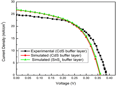 |
| | Fig. 2 Comparison of experimental and simulated J–V curves of Sb2Se3-based solar cells. | |
Table 4 Comparison of electrical parameters of Sb2Se3-based photovoltaic
| Solar cell |
VOC (V) |
JSC (mA cm−2) |
FF (%) |
ƞ (%) |
| Experimental73 |
0.386 |
24.6 |
54.5 |
5.17 |
| Simulated20 |
0.362 |
27.51 |
51.95 |
5.17 |
| Simulated (this work) (CdS buffer layer) |
0.358 |
26.71 |
54.05 |
5.17 |
| Simulated (this work) (SnS2 buffer layer) |
0.362 |
26.89 |
54.02 |
5.25 |
3.2 Impact of Sb2Se3 absorber layer thickness
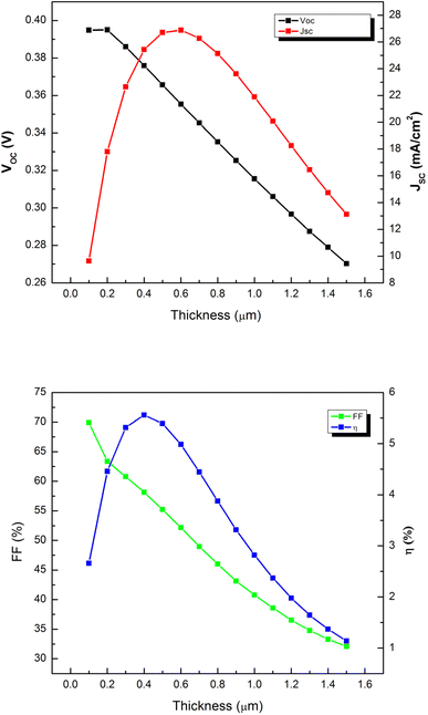
An optimal absorber layer thickness ensures that photo-generated electron–hole pairs reach their respective contacts without recombination. The influence of the Sb2Se3 absorber layer thickness is examined by tuning absorber layer thickness from 0.1–1.5 µm, while different layers material parameters are kept unchanged. Solar cell output corresponding to absorber layer thickness variation are shown in Fig. 3. It is observed that JSC increases from 9.63 mA cm−2 to 26.88 mA cm−2 as absorber layer thickness is increased from 0.1–0.6 µm due to increase in electron–hole pair generation. Afterwards it starts decreasing due to recombination and reaches 13.13 mA cm−2 as absorber layer thickness is enhanced to 1.5 µm. VOC remains almost constant at 0.395 V as absorber layer thickness is enhanced from 0.1–0.2 µm. Then, it starts decreasing due to recombination and reaches 0.27 V as absorber layer thickness is enhanced to 1.5 µm.87,88 FF decreases from 69.9–32.1% because of rise in series resistance as absorber layer thickness is increased from 0.1–1.5 µm. The combined impact of FF, VOC and JSC cause efficiency to rise from 2.66–5.56% as absorber layer thickness is increased from 0.1–0.4 µm. Then efficiency starts to decline as absorber layer thickness is increased and reaches 1.14% as absorber layer thickness is enhanced to 1.5 µm. A thin absorber layer results in low both JSC and efficiency due to reduction of absorption capacity of light. Enhancement of absorber layer thickness increases efficiency of the solar cell due to large number of photons being absorbed and rise in carrier generation.14 Efficiency declines as absorber layer thickness is enhanced above 0.4 µm due to recombination as the path length covered by photo-generated carriers become very large.89 So absorber layer thickness is optimized at 0.4 µm which falls within range published in previous works.12,34
 |
| | Fig. 3 Impact of Sb2Se3 absorber layer thickness on solar cell electrical parameters. | |
3.3 Influence of Sb2Se3 absorber layer carrier density
The effect of the Sb2Se3 absorber layer carrier density on device output is examined and simulation outcomes are displayed in Fig. 4. The Sb2Se3 absorber layer acceptor density is tuned from 1012–5 × 1016 cm−3. VOC increases from 0.38 V to 0.41 V and FF rises from 58.12–66.36% as absorber layer acceptor concentration is increased in considered range. JSC increases slightly from 25.43 mA cm−2 to 25.86 mA cm−2 as doping density is tuned from 1012–1016 cm−3 after which it starts decreasing. An enhanced doping density results in rise in the bulk and interface recombination rate, thereby declining JSC.54 The combined effect of VOC, JSC and FF causes efficiency to rise from 5.56–6.31% with increase in acceptor concentration from 1012–1016 cm−3. Afterwards, efficiency degrades. Increase in the carrier density creates the built-in potential at the interface which decreases the recombination and rises the efficiency up to a certain limit.90 Additional hole recombination centers created at high doping density in the absorber due to increased acceptor impurity increase recombination and declines efficiency.14 So the optimal absorber layer doping density chosen is 1016 cm−3 which is within doping concentration value used in previous works.12,37
 |
| | Fig. 4 Impact of Sb2Se3 absorber layer acceptor concentration on device performance. | |
3.4 Effect of Sb2Se3 absorber layer defect density
The defect density of the absorber layer which are inevitable during the fabrication plays a vital role in impacting the performance of solar cells. Defects in the absorber layer results from antisite defects, point defects, crystal imperfections and interstitials. The effect of the Sb2Se3 absorber layer defect density is examined and outcomes are depicted in Fig. 5. The Sb2Se3 absorber layer defect density is altered from 1010–1015 cm−3. Both VOC and JSC remain almost fixed up to defect density of 1012 cm−3. Thereafter, both decline significantly as defect density is increased in considered range. FF and ƞ remain unaltered as defect density is increased from 1010–1011 cm−3. Then both decrease significantly. It is observed that JSC, VOC, FF and ƞ decrease from 27.86 mA cm−2 to 3.94 mA cm−2, 0.49 V to 0.126 V, 74.58–33.13%, and 10.14–0.16% respectively as defect density is increased from 1010–1015 cm−3. Increase in absorber layer defect density causes increase in Shockley Read Hall (SRH) recombination of carriers which reduces the carrier lifetime and diffusion length.14,91,92 As a result, the production of electron–hole is reduced due to prevention of the carriers from reaching the junctions which degrades the solar cell performance parameters.93 The absorber layer defect density selected is 1013 cm−3 for maximum efficiency which is in good agreement with research works.17,53
 |
| | Fig. 5 Impact of Sb2Se3 absorber layer defect density on solar cell output. | |
3.5 Optimization of Sb2Se3 absorber layer bandgap
The effect of the Sb2Se3 absorber layer bandgap is examined by altering absorber layer bandgap from 1–1.3 eV. Solar cell output parameter changes corresponding to absorber layer bandgap variation are depicted in Fig. 6. It is observed that JSC decreases from 26.4 mA cm−2 to 17.57 mA cm−2 as bandgap rises from 1 to 1.3 eV. VOC increases from 0.375 V to 0.64 V with rise in bandgap in considered range due to decline in radiative recombination rate.94 Both FF and ƞ rise up to bandgap of 1.15 eV. Afterwards, both degrade with rise in bandgap. The generated rate of carriers is enhanced due to improved absorber/buffer junction which causes efficiency to increase as bandgap rises from 1 to 1.15 eV.95 The mismatch between Sb2Se3 and SnS2 bandgap creates recombination centers which increases carriers' recombination with further increase of Sb2Se3 bandgap above 1.15 eV and declines efficiency.96 So the absorber layer bandgap is optimized at 1.15 eV at which ƞ reaches 6.96%.
 |
| | Fig. 6 Solar cell characteristics with respect to Sb2Se3 absorber layer bandgap. | |
3.6 Effect of SnS2 buffer layer thickness
The influence of SnS2 buffer layer thickness on solar cell output parameters is also explored. The thickness is tuned from 0.01–0.1 µm. Fig. 7 displays the simulation findings obtained. It is observed that both VOC and JSC decrease and FF remains almost constant as buffer layer thickness is enhanced in considered range. The photo-generated carriers need to travel longer distance to go to the active region with the rise in the thickness of buffer layer which increases the recombination rate which in turn decreases both JSC and VOC.97 The efficiency decreases from 7.34–6.6% as buffer layer thickness is varied from 0.01–0.1 µm. Less number of photons reach the Sb2Se3 layer which led to reduction of the production of electron–hole pair with increase in the thickness of SnS2 layer due to the increase in absorption of photons in the buffer layer which declines efficiency.93 When the SnS2 layer is very thin, the space charge width of the junction is decreased and the pinholes might be created so that Sb2Se3 directly connects to the front contact.20 So the optimal buffer layer thickness chosen is 0.03 µm which is also used in published researches.98,99
 |
| | Fig. 7 Impact of SnS2 buffer layer thickness on cell performance parameters. | |
3.7 Influence of SnS2 buffer layer donor density
The effect of the SnS2 buffer layer donor concentration is examined and simulation findings are displayed in Fig. 8. The SnS2 buffer layer donor density is altered from 1013–1018 cm−3. FF declines as donor density is enhanced in considered range. VOC and JSC increase from 0.45 V to 0.51 V and 15.36 mA cm−2 to 22.44 mA cm−2 respectively which causes ƞ to rise from 5.86–7.14% as buffer layer carrier density is enhanced from 1013–1018 cm−3. At low carrier concentration, the depletion region extends out of the buffer layer thickness and the diode behavior of the device is decreased.48 The electric field on the Sb2Se3/SnS2 junction and the SnS2//FTO junction rise which augments the separation of the photo-generated charges and efficiency with rise in buffer layer doping concentration.100 So the buffer layer donor density is optimized at 1018 cm−3 which is compatible with published work.48
 |
| | Fig. 8 Photovoltaic output as a function of SnS2 buffer layer donor concentration. | |
3.8 Effect of SnS2 buffer layer defect density
To examine the influence of SnS2 buffer layer defect density on photovoltaic characteristics, the defect density is altered from 1010–1018 cm−3 and photovoltaic output changes obtained are displayed in Fig. 9. All the electrical parameters remain almost constant up to defect density of 1017 cm−3. Thereafter, all parameters start to degrade drastically. FF starts increasing particularly at 1017 cm−3 because of rise in energy barrier height.93,101 The efficiency decreases from 7.12–5.87% as defect density is increased from 1017–1018 cm−3. The enhanced defect density reduces the carriers' diffusion length and life time and as a result, efficiency decreases as photo-generated carriers find it hard to travel.102 So buffer layer defect density of 1015 cm−3 is chosen as optimum value which matches with previous work.12
 |
| | Fig. 9 Effect of SnS2 buffer layer defect density on photovoltaic output. | |
3.9 Effect of FTO window layer thickness
The influence of FTO window layer thickness on solar cell output is also simulated. The thickness is altered from 0.1–0.6 µm. Fig. 10 displays the simulation outcomes obtained. It is observed that both VOC and JSC decrease very slightly and FF remains almost constant as window layer thickness is enhanced within 0.1–0.6 µm. The efficiency decreases from 7.16–7.13% as window layer thickness is varied from 0.1–0.6 µm. As FTO layer thickness rises, the absorption of a large part of the light which incidents in the FTO layer declines transmission, which creates an optical loss and as a result degrades efficiency in the solar cell.103 So the optimal window layer thickness chosen is 0.1 µm.
 |
| | Fig. 10 Impact of FTO window layer thickness on cell output parameters. | |
3.10 Influence of FTO window layer doping concentration
The effect of the FTO window layer donor concentration is examined and simulation results are outlined in Fig. 11. The FTO window layer doping concentration is tuned from 1017–1020 cm−3. VOC remains constant and both FF and JSC increase with increase in window layer donor concentration in considered range. Efficiency increases very slightly from 7.16–7.21% as window layer donor concentration is increased from 1017–1020 cm−3. It is concluded that the FTO layer doping density has insignificant effect on the performance of the proposed Sb2Se3 based solar cell when compared to the effect of the absorber and buffer layer. The photo-generated carries may be collected by electrodes efficiently with rise of FTO layer donor density and thus increases efficiency.104 The optimal window layer donor density chosen is 1020 cm−3 which is compatible with research work.105
 |
| | Fig. 11 Impact of FTO window layer donor density on device performance. | |
3.11 Effect of Sb2Se3/SnS2 interface defect density
Metallurgical discontinuities, lattice mismatch and symmetry breaking at the interfaces result in interface defects. Interface with low lattice mismatch results in low both interfacial defects and recombination rate and enhances performance parameters. The Sb2Se3/SnS2 interface defect density is altered from 107 cm−2 to 1018 cm−2 to investigate its impact on device output. Simulation findings are depicted in Fig. 12. It is observed that all performance parameters decrease significantly as interface defect density is increased from 107 cm−2 to 1010 cm−2. Afterwards, all performance parameters remain nearly constant. The VOC, JSC, FF and efficiency decreases from 0.52 V to 0.5135 V, 24.19 mA cm−2 to 22.52 mA cm−2, 63.3–62.36% and 7.96–7.21% respectively as interface defect density is increased from 107–1018 cm−2. Enhanced recombination centers at the Sb2Se3/SnS2 interface due to increase in electron trap centers at high density of Sb2Se3/SnS2 interface defects are responsible for the degradation of performance parameters.106 The optimal Sb2Se3/SnS2 interface defect density selected is 1010 cm−2 which is in good agreement with earlier research works.107,108
 |
| | Fig. 12 Influence of Sb2Se3/SnS2 interface defect density on cell output. | |
3.12 Effect of Sb2Se3 absorber layer capture cross section
The influence of the Sb2Se3 absorber layer capture cross section is investigated by altering the Sb2Se3 absorber layer electron and hole capture cross section from 10−19–10−9 cm−2. Simulation results are displayed in Fig. 13. It is observed that both VOC and JSC remain almost constant as capture cross section is enhanced from 10−19–10−12 cm−2. Then both decrease as capture cross section is increased in considered range. Both FF and ƞ remain unaltered as capture cross section is enhanced from 10−19–10−13 cm−2. Afterwards, both decline as capture cross section is increased in considered range. Efficiency decreases from 10.23–1.24% as capture cross section is enhanced from 10−19–10−9 cm−2. Both carrier diffusion length and lifetime is declined because of large lattice mismatch and enhancement of recombination rate as capture cross-section of defect is increased which degrades device performance parameters.109,110 The optimal Sb2Se3 absorber layer capture cross section selected is 10−15 cm−2 which matches with reported earlier work.12
 |
| | Fig. 13 Effect of Sb2Se3 absorber layer capture cross-section on device electrical parameters. | |
3.13 The influence of Sb2Se3/SnS2 interface capture cross-section
The Sb2Se3/SnS2 interface capture cross section of electron and hole is tuned from 10−20–10−8 cm−2 to examine its impact on device output and simulation results are depicted in Fig. 14. It is observed that all performance parameters remain almost constant as capture cross section is enhanced from 10−20–10−13 cm−2. Then all parameters decline as capture cross section is increased in considered range. Efficiency decreases from 12.31–10.18% as capture cross section is enhanced from 10−20 cm−2 to 10−8 cm−2. It is evident that interface capture cross-section has less effect on device output compared to absorber capture cross-section of carriers. Enhancement in capture cross-section of electron and hole results in degradation of the Sb2Se3/SnS2 interface quality, enhancement in recombination and as a result, the efficiency declines.111,112 The optimal Sb2Se3/SnS2 interface capture cross section chosen is 10−19 cm−2 which is compatible with research work.111
 |
| | Fig. 14 Solar cell characteristics as a function of Sb2Se3/SnS2 interface capture cross-section. | |
3.14 Impact of SnS BSF layer thickness
The BSF layer allows easy transportation of holes and blocks the electrons to the back contact simultaneously. Thus BSF layer has a major role in solar cell performance. The effect of SnS BSF layer thickness on solar cell characteristics is also explored. The thickness is varied from 0.02–0.2 µm. Device performance changes with respect to SnS thickness variation are displayed in Fig. 15. The acceptor concentration and defect density of BSF layer is maintained fixed at 1018 cm−3 and 1014 cm−3 respectively. It is observed that the thickness of SnS shows significant effect on the solar cell performance parameters. VOC, JSC, FF and ƞ increases from 0.7 V to 0.83 V, 26.76 mA cm−2 to 31.91 mA cm−2, 80.97–85.96% and 15.12–22.87% as SnS BSF layer thickness is increased from 0.02–0.2 µm. The decrease of recombination rate of carriers with increasing BSF thickness improves both VOC and JSC.105 The generation of carriers is increased with the rise in the thickness of BSF layer with the same amount of incident photon and thus improves efficiency.91 To minimize production cost and the quantity of material used by the absorber layer, the optimal SnS BSF layer thickness chosen is 0.2 µm which matches with reported study.98
 |
| | Fig. 15 Effect of SnS BSF layer thickness on device characteristics. | |
3.15 Influence of SnS BSF layer acceptor concentration
The effect of the SnS BSF layer acceptor density is examined and simulation outcomes are represented in Fig. 16. The SnS BSF layer doping concentration is tuned from 1015–1020 cm−3. All electrical parameters except FF enhance with rise in SnS BSF layer carrier density from 1015–1020 cm−3. FF increases from 72.65–85.96% as SnS BSF layer acceptor concentration is enhanced from 1015–1018 cm−3 due to decrease in series resistance. Afterwards, FF decline due to increase of recombination at high doping. VOC, JSC and efficiency increases from 0.66 V to 0.94 V, 26.6 mA cm−2 to 31.98 mA cm−2 and 12.74–24.86% as doping density of BSF layer is increased from 1015–1020 cm−3. The large potential created at the SnS/Sb2Se3 interface reduces recombination rate of carriers at high carrier density of BSF layer. Ohmic contact is created with the back contact due to closeness of BSF Fermi level with the valence band (VB) at high BSF doping density which supports easy transportation of holes towards back electrode and enhances device performance.113 The optimal BSF layer acceptor density chosen is 1020 cm−3. The result is within range of earlier simulation studies.37,114
 |
| | Fig. 16 Impact of SnS BSF layer acceptor density on photovoltaic output. | |
3.16 Effect of SnS BSF layer defect density
The SnS BSF layer defect density is varied from 1010–1020 cm−3 to examine its impact on device electrical parameters and simulation outcomes are displayed in Fig. 17. The efficiency is nearly fixed till defect density of 1017 cm−3. Afterwards, efficiency starts to degrade. The efficiency declines from 24.86–12.79% as defect density is enhanced from 1010–1020 cm−3 due to increase in recombination. The sudden rise in FF from defect density 1017–1019 cm−3 is due to increase in energy barrier height.93,101 The optimal BSF layer defect density selected is 1014 cm−3 which matches with earlier study.114
 |
| | Fig. 17 Influence of SnS BSF layer defect density on cell output parameters. | |
3.17 Impact of back contact work function
The back contact work function majorly impacts the efficiency of the solar cell. A high work function back contact is needed for a proper ohmic contact at the absorber or BSF/back contact interface. To explore the influence of back contact on photovoltaic output, back contact work function is tuned from 4.5–5.4 eV and simulation outcomes obtained are represented in Fig. 18. JSC increases by a small margin as work function is enhanced within 4.5–5.4 eV. Both VOC and FF enhance prior to work function of 5 eV and thereafter stay almost saturated. The combined increase of VOC and FF enhances the efficiency till work function of 5 eV and then remain saturated. With rise in work function of the back electrode, the carriers' barrier height at the back surface decreases which enhances device performance.14 So for maximum efficiency of proposed solar cell, back electrode work function is required to be larger or equal to 5 eV.
 |
| | Fig. 18 Impact of back contact work function on device performance with BSF layer. | |
3.18 Impact of temperature
Long-term stability under ambient air condition is a major requirement for the application of photovoltaic device. The influence of the working temperature on solar cell is investigated in a range of 300–400 K and the simulation outcomes are depicted in Fig. 19. JSC increases slightly due to reduction of the bandgap of the absorber which rises the generation of carrier in solar cell as temperature is increased in considered range.115 The rise of temperature makes thermally generated electrons unstable due to vibration and recombine with the holes before being collected at the electrodes, reducing VOC linearly. Moreover, the rise in temperature impacts the carrier properties such as mobility and carrier density and as a result, declines the FF of device.116 The combined decrease in VOC and FF declines efficiency from 24.86–20.37% as temperature is enhanced from 300–400 K.
 |
| | Fig. 19 Solar cell output variation with changes in temperature with BSF layer. | |
3.19 Influence of parasitic resistance
Series resistance (RS) and shunt resistance (RSh) have a vital effect on photovoltaic output. The solar cell performs best at maximum RSh and minimum Rs values. RS is the sum of resistance between different layers of solar cells and at the back and front contacts.117 When the current created by sunlight flows through the various channels produced by small RSh, efficiency degrades.14
The Sb2Se3 solar cell performance parameters with SnS BSF layer is investigated by varying the RS from 0 to 8 Ω cm2. The obtained results are shown in Fig. 20. It is observed that VOC remains constant and JSC decreases slightly with rise of series resistance. JSC decreases because of rise in internal resistance which impedes the transport of carriers to the contacts.118 FF decreases significantly from 83.09–59.1% with increase of series resistance in considered range. As a result, efficiency decreases from 24.86–17.68% for optimized FTO/SnS2/Sb2Se3/SnS/Au solar cell as RS is increased from 0 to 8 Ω cm2. Rs should be kept as low as possible to achieve high efficiency.
 |
| | Fig. 20 Effect of series resistance (RS) on cell output parameters with BSF layer. | |
The RSh is changed from 200 Ω cm2 to 1600 Ω cm2 to investigate its effect on the cell output with SnS BSF layer and findings are shown in Fig. 21. JSC is found to be unaltered, VOC increases slightly and FF rises significantly with increase of shunt resistance in considered range. Efficiency rises from 21.6–24.45% as shunt resistance is increased from 200–1600 Ω cm2 for proposed Sb2Se3 solar cell with SnS BSF layer mainly due to rise of FF. FF increases with increase in RSh because of low recombination rates.119 It is observed that both FF and efficiency rise with increase in the RSh till 1200 Ω cm2 and almost saturate on further increase in RSh. As a result, RSh should be high to achieve high efficiency.
 |
| | Fig. 21 Impact of shunt resistance (RSh) on solar cell characteristics with BSF layer. | |
3.20 Overall cell performance
The influence of inserting highly doped p-type SnS BSF layer of Sb2Se3 based solar cell on the current density–voltage (J–V) is depicted in Fig. 22. The electrical parameters of Sb2Se3 based solar cell without and with SnS BSF layer are summarized in Table 5. The optimum parameters of different layers of FTO/SnS2/Sb2Se3/SnS/Au solar cell are illustrated in Table 6. The optimized FTO/SnS2/Sb2Se3/Au solar cell structure obtains VOC, JSC, FF and ƞ of 0.66 V, 25.59 mA cm−2, 73.33% and 12.31% respectively. The insertion of SnS BSF layer enhances VOC, JSC, FF and ƞ to 0.94 V, 31.98 mA cm−2, 83.09% and 24.86% respectively. It is noticed that all electrical parameters are enhanced due to addition of SnS BSF layer. The creation of large built-in potential at the Sb2Se3/SnS interface rises the value of VOC.120 The efficient separation and collection of carriers due to the addition of BSF layer enhances the value of JSC.121 The improvement of FF is due to rise in the maximum power produced by FTO/SnS2/Sb2Se3/SnS/Au solar cell structure due to reduction of recombination rate at back surface due to the insertion of SnS BSF layer.122 The efficiency has significantly enhanced due to the insertion of SnS BSF layer because of combined increment of VOC, JSC and FF.
 |
| | Fig. 22 J–V characteristic curve of Sb2Se3 based photovoltaic with and without SnS BSF layer. | |
Table 5 Performance parameters of the proposed FTO/SnS2/Sb2Se3/Au solar cell structure without and with SnS BSF layer
| Structure |
VOC (V) |
JSC (mA cm−2) |
FF (%) |
ƞ (%) |
| FTO/SnS2/Sb2Se3/Au |
0.66 |
25.59 |
73.33 |
12.31 |
| FTO/SnS2/Sb2Se3/SnS/Au |
0.94 |
31.98 |
83.09 |
24.86 |
Table 6 Optimized parameter values of the FTO/SnS2/Sb2Se3/SnS/Au solar cell
| Optimized parameter |
Value |
| Sb2Se3 absorber layer thickness |
0.4 µm |
| Sb2Se3 absorber layer acceptor concentration |
1016 cm−3 |
| Sb2Se3 absorber layer defect density |
1013 cm−3 |
| Sb2Se3 absorber layer bandgap |
1.15 eV |
| SnS2 buffer layer thickness |
0.03 µm |
| SnS2 buffer layer donor concentration |
1018 cm−3 |
| SnS2 buffer layer defect density |
1015 cm−3 |
| FTO window layer thickness |
0.1 µm |
| FTO window layer donor concentration |
1020 cm−3 |
| Sb2Se3/SnS2 interface layer defect density |
1010 cm−2 |
| Sb2Se3 absorber layer capture cross-section of electron and hole |
10−15 cm−2 |
| Sb2Se3/SnS2 interface capture cross-section of electron and hole |
10−19 cm−2 |
| SnS BSF layer thickness |
0.2 µm |
| SnS BSF layer acceptor concentration |
1020 cm−3 |
| SnS BSF layer defect density |
1014 cm−3 |
| Back contact work function |
5 eV |
The quantum efficiency (QE) curve for Sb2Se3 based solar cell at initial and with optimization with and without SnS BSF layer is displayed in Fig. 23. The strong back surface electric fields at the SnS/Sb2Se3 interface due to addition of SnS BSF layer in the simulated cell structure decreases carrier recombination and increases the absorption at the wavelength range from 400 to 1030 nm, which increases the electrical parameters of the designed photovoltaic. This results prove that SnS can be a potential BSF layer for improving the efficiency of Sb2Se3-based photovoltaic.
 |
| | Fig. 23 QE characteristic curve of Sb2Se3 based photovoltaic with and without SnS BSF layer. | |
In this research, a promising efficiency of 24.86% was obtained by incorporating SnS as a BSF layer due to n-SnS2/p-Sb2Se3/p+-SnS forming of n–p–p+ double heterojunction cell. This double junction cell efficiency improvement can be demonstrated by Tail-States-Assisted (TSA) two-steps photon upconversion process. In this double heterostructure, with the insertion of SnS BSF layer, the sub-bandgap photons may get absorbed notably, specifically in the longer wavelength, which causes an enhancement in solar cell performance. The sub-bandgap photons may be absorbed by the Urbach energy states and these lower energy sub-bandgap photons participate in tail-state-assisted (TSA) two-steps photon upconversion.107,123,124 These absorbed photons generate additional electron–hole pairs, resulting in a noticeable improvement in cell photocurrent. A photoactive material such as SnS BSF layer can cause this TSA upconversion effectively when it possesses favorable bandgap, high absorption coefficient and adequate doping concentration.105,125 Thus, it is believed that this is the main reason of the high-efficiency of 24.86% observed in proposed double heterojunction solar cell. The Urbach energy, E0, of the photoactive material determines the resulting increase in photocurrent and the degree of upconversion. The higher Urbach energy remarkably promotes to boosting the quantum efficiency (QE), specifically in the longer wavelength.5,126
The energy band diagram of the optimized Sb2Se3-based solar cell architecture of FTO/SnS2/Sb2Se3/SnS/Au is displayed in Fig. 24. It is noticed that the energy level of conduction and valence band of SnS2 buffer layer is lower than the Sb2Se3 absorber layer. As a result, electrons can travel easily to the front contact through the Sb2Se3/SnS2 interface due to small conduction band offset (CBO) of −0.05 eV. On the other hand, the valence band offset (VBO) between the SnS2 buffer layer and Sb2Se3 absorber layer is large enough to prevent the flow of holes from Sb2Se3 absorber to front contact. For the SnS BSF layer, the energy level of valence and conduction band is higher than the Sb2Se3 absorber layer. Moreover, a proper barrier height with a suitable conduction band offset (CBO) at the SnS BSF/Sb2Se3 absorber junction hinders electrons from travelling from the absorber to the back electrode which in turn reduces recombination process at the back surface.14,98 On the contrary, the holes can travel from absorber to the back contact easily due to small VBO of 0.1 eV.
 |
| | Fig. 24 Energy band diagram of proposed FTO/SnS2/Sb2Se3/SnS/Au solar cell. | |
3.21 Comparative study
Table 7 compares various results from past experimental or theoretical work on Sb2Se3 based solar cells with various buffer layers without and with BSF layer. In comparison to the previous reported values, enhanced ƞ have been achieved by this simulation study.
Table 7 Comparison of proposed solar cell with other reported Sb2Se3 based solar cells
| Structure |
Study type |
Photovoltaic parameters |
References |
| VOC (V) |
JSC (mA cm−2) |
FF (%) |
ƞ (%) |
| FTO/CdS/Sb2Se3/CZTA/Au |
Experimental |
0.421 |
28.40 |
57.10 |
6.84 |
73 |
| Ag/ITO/ZnO/CdS/Sb2Se3/Mo/SLG |
Experimental |
0.454 |
18.4 |
50.6 |
4.22 |
127 |
| Ag/ITO/CdS/Sb2Se3/Mo |
Experimental |
0.343 |
16.79 |
35.3 |
2.1 |
128 |
| FTO/CdS/Sb2Se3/Spiro-OMeTAD/Au |
Experimental |
0.360 |
29.00 |
51.50 |
5.40 |
55 |
| ITO/CdS/Sb2Se3/Au |
Experimental |
0.379 |
27.93 |
55.6 |
5.91 |
129 |
| AZO/i-ZnO/CdS/TiO2/Sb2Se3/Mo |
Experimental |
0.4 |
32.58 |
70.30 |
9.20 |
19 |
| ITO/CdS/Sb2Se3/CuSCN/Au |
Experimental |
0.413 |
30.51 |
58.99 |
7.5 |
130 |
| ITO/CdS/Sb2Se3/Au |
Experimental |
0.420 |
29.90 |
60.40 |
7.60 |
26 |
| Metal contact/ZnO:Al/i-ZnO/CdS/Sb2Se3/Mo |
Simulation |
0.56 |
31.79 |
70.81 |
12.62 |
33 |
| ZnO:Al/ZnO/CdS/TiO2/Sb2Se3/MoS2/Mo |
Simulation |
0.4 |
32.56 |
70.3 |
9.17 |
131 |
| FTO/Zn(Sn,O)/Sb2Se3/CZTSe/Au |
Simulation |
0.66 |
34.66 |
81.18 |
18.50 |
132 |
| Ag/phenyl-C61-butyric acid methyl ester (PCBM)/Sb2Se3/HTL/ITO |
Simulation |
0.858 |
34.18 |
84.04 |
24.66 |
133 |
| Ag/ZnSe/Sb2Se3/Mo |
Simulation |
0.85 |
34 |
83.6 |
24.0 |
17 |
| Al/ITO/CdS/Sb2Se3/CuS/Ni |
Simulation |
0.761 |
37.59 |
80.97 |
23.16 |
12 |
| FTO/SnS2/Sb2Se3/Au |
Simulation |
0.66 |
25.59 |
73.33 |
12.31 |
This work |
| FTO/SnS2/Sb2Se3/SnS/Au |
Simulation |
0.94 |
31.98 |
83.09 |
24.86 |
This work |
4. Conclusions
The electrical parameters of Sb2Se3-based thin film solar cell with and without SnS BSF layer have been compared in this simulation work using SCAPS-1D. First of all, experimental result is reproduced for FTO/CdS/Sb2Se3/Au solar cell structure to validate the numerical model and carry out analysis. Next, non-toxic SnS2 has been used as a buffer layer instead of the hazardous cadmium sulfide (CdS) for the proposed solar cell which results in enhanced efficiency. Afterwards, to maximize efficiency different parameters such as thickness, doping concentration, bandgap, capture cross section and defect density that effect the electrical output is optimized. The optimal thickness for the Sb2Se3 absorber layer, SnS2 buffer layer and FTO window layer have been chosen to be of 0.4 µm, 0.03 µm and 0.1 µm respectively. The doping density have been optimized to be of 1016 cm−3, 1018 cm−3 and 1020 cm−3 respectively. The defect density in the Sb2Se3 absorber layer, SnS2 buffer layer and the interface defect at Sb2Se3/SnS2 interface have been selected to be of 1013 cm−3, 1015 cm−3 and 1010 cm−2 respectively for optimal performance. The capture cross-section in the Sb2Se3 absorber layer and at Sb2Se3/SnS2 interface have been optimized to be of 10−15 cm−2 and 10−19 cm−2 respectively. The optimized FTO/SnS2/Sb2Se3/Au solar cell structure provides JSC of 25.59 mA cm−2, VOC of 0.66 V, FF of 73.33% and efficiency of 12.31%. The insertion of SnS BSF layer with thickness of 0.2 µm, carrier density of 1020 cm−3 and defect density of 1014 cm−3 results in enhanced efficiency of 24.86% including JSC of 31.98 mA cm−2, VOC of 0.94 V and FF of 83.09% for optimized novel FTO/SnS2/Sb2Se3/SnS/Au solar cell structure. The findings of this simulation work provide guidelines for the production of non-toxic, cost-effective and highly efficient Sb2Se3-based solar cell.
Conflicts of interest
The author declares that there is no conflict of interest regarding the publication of this paper.
Data availability
The data will be made available on reasonable request.
Acknowledgements
This research did not receive any specific grant from funding agencies in the public, commercial, or not-for-profit sectors. The author is grateful to Dr Marc Burgelman at University of Ghent, Belgium for allowing to use the SCAPS-1D simulation package.
References
- S. Saurabh, M. K. Hossain, S. Singh, S. K. Agnihotri and D. P. Samajdar, Optical performance analysis of InP nanostructures for photovoltaic applications, RSC Adv., 2023, 13, 9878–9891 Search PubMed.
- M. R. Islam, M. S. Islam, M. Y. Zamil, N. Ferdous, C. Stamp, J. Park and M. K. Hossain, Two-dimensional BAs/GeC van der waals heterostructures: A widely tunable photocatalyst for water splitting and hydrogen production, J. Phys. Chem. Solids, 2023, 176, 111263 Search PubMed.
- M. Shahbaz, A. Siddiqui, M. Siddiqui, Z. Jiao and P. Kautish, Exploring the growth of sustainable energy Technologies: A review, SUSTAIN, 2023, 57, 103157 Search PubMed.
- M. H. K. Rubel, S. K. Mitro, M. K. Hossain, K. M. Hossain, M. M. Rahaman, J. Hossain, B. K. Mondal, A. Akter, M. F. Rahman, I. Ahmed and A. K. M. A. Islam, First-principles calculations to investigate physical properties of single-cubic (Ba0.82K0.18)(Bi0.53Pb0.47)O3 novel perovskite superconductor, Mater. Today Commun., 2022, 33, 104302 CrossRef CAS.
- J. A. Mahmud, M. F. Rahman, A. Kuddus, M. H. Ali, A. T. M. S. Islam, M. D. Haque, S. R. A. Ahmed, M. Mushtaq and A. B. M. Ismail, Design and analysis of SnS2/WS2/V2O5 double-heterojunction toward high performance photovoltaics, Energy Adv., 2023, 2, 1843–1858 RSC.
- A. Laidouci, M. Lamba, V. N. Singh, P. K. Dakua and D. K. Panda, Performance evaluation of ZnSnN2 solar cells with Si back surface field using SCAPS-1D: a theoretical study, Heliyon, 2023, 9, e20601 Search PubMed.
- M. E. Islam, M. R. Islam, S. Ahmmed, M. K. Hossain and M. F. Rahman, Highly Efficient SnS-Based Inverted Planar Heterojunction Solar Cell with ZnO ETL, Phys. Scr., 2023, 98, 065501 Search PubMed.
- S. Kashyap, J. Madan, M. K. A. Mohammed, M. Khalid Hossain, S. Ponnusamy and R. Pandey, Unlocking the potential of MgF2 textured surface in enhancing the efficiency of perovskite solar cells, Mater. Lett., 2023, 339, 134096 CrossRef CAS.
- S.-C. Yang, T.-Y. Lin, M. Ochoa, H. Lai, R. K. Kothandaraman, F. Fu, A. N. Tiwari and R. Carron, Efficiency boost of bifacial Cu(In,Ga)Se2 thin-film solar cells for flexible and tandem applications with silver-assisted low-temperature process, Nat. Energy, 2023, 8, 40–51 Search PubMed.
- N. Shrivastav, S. Kashyap, J. Madan, A. K. Al-Mousoi, M. K. A. Mohammed, M. K. Hossain, R. Pandey and J. Ramanujam, Perovskite-CIGS monolithic tandem solar cells with 29.7% efficiency: A numerical study, Energy Fuels, 2023, 37, 3083–3090 CrossRef CAS.
- M. A. Islam, A. Jawad, N. A. Jahan and M. M. Hossain, Outstanding conversion efficiency of 38.39% from a Perovskite/CIGS tandem PV cell: A synergic optimization through computational modeling, Heliyon, 2023, 9, e20558 CrossRef CAS.
- A. E. Khalfi, M. Ouhadou, I. Rais, F. Essahlaoui, M. F. Rahman, M. Sahal, L. Elmaimouni and A. Benami, A numerical approach to maximizing efficiency in Sb2Se3 solar cells by using CuS as a hole transport material, Eur. Phys. J. Plus, 2023, 138, 1085 Search PubMed.
- M. A. Mughal, R. Engelken and R. Sharma, Progress in indium (III) sulfide (In2S3) buffer layer deposition techniques for CIS, CIGS, and CdTe-based thin film solar cells, Sol. Energy, 2015, 120, 131–146 CrossRef CAS.
- B. Islam, A. Hosen, T. M. Khan, M. F. Rahman, M. H. Rahman, M. S. Islam and S. R. A. Ahmed, Simulating the effect of inserting Sb2S3 as hole transport layer on SnS-based thin-film solar cells, J. Electron. Mater., 2024, 53, 4726–4739 Search PubMed.
- W. Wang, M. T. Winkler, O. Gunawan, T. Gokmen, T. K. Todorov, Y. Zhu and D. B. Mitzi, Device characteristics of CZTSSe thin-film solar cells with 12.6% efficiency, Adv. Energy Mater., 2014, 4, 1301465 CrossRef.
- C. Chen, L. Wang, L. Gao, D. Nam, D. Li, K. Li, Y. Zhao, C. Ge, H. Cheong, H. Liu, H. Song and J. Tang, 6.5% certified efficiency Sb2Se3 solar cells using PbS colloidal quantum dot film as hole-transporting layer, ACS Energy Lett., 2017, 2, 2125–2132 CrossRef CAS.
- R. Kumari, M. Mamta, R. Kumar, Y. Singh and V. N. Singh, 24% efficient, simple ZnSe/Sb2Se3 heterojunction solar cell: An analysis of PV characteristics and defects, ACS Omega, 2023, 8, 1632–1642 CrossRef CAS.
- L. Wang, D.-B. Li, K. Li, C. Chen, H.-X. Deng, L. Gao, Y. Zhao, F. Jiang, L. Li, F. Huang, Y. He, H. Song, G. Niu and J. Tang, Stable 6%-efficient Sb2Se3 solar cells with a ZnO buffer layer, Nat. Energy, 2017, 2, 17046 Search PubMed.
- Z. Li, X. Liang, G. Li, H. Liu, H. Zhang, J. Guo, J. Chen, K. Shen, X. San, W. Yu, R. E. I. Schropp and Y. Mai, 9.2%-efficient core-shell structured antimony selenide nanorod array solar cells, Nat. Commun., 2019, 10, 125 Search PubMed.
- A. T. Ngoupo, S. Ouedraogo, F. Zougmore and J. M. B. Ndjaka, Numerical analysis of ultrathin Sb2Se3-based solar cells by SCAPS-1D numerical simulator device, Chin. J. Phys., 2021, 70, 1–13 CrossRef CAS.
- Y. Lai, Z. Chen, C. Han, L. Jiang, F. Liu, J. Li and Y. Liu, Preparation and characterization of Sb2Se3 thin films by electrodeposition and annealing treatment, Appl. Surf. Sci., 2012, 261, 510–514 CrossRef CAS.
- Y. Zhou, L. Wang, S. Chen, S. Qin, X. Liu, J. Chen, D. J. Xue, M. Luo, Y. Cao, Y. Cheng, E. H. Sargent and J. Tang, Thin-film Sb2Se3 photovoltaics with oriented one-dimensional ribbons and benign grain boundaries, Nat. Photonics, 2015, 9, 409–415 CrossRef CAS.
- S. Messina, M. T. S. Nair and P. K. Nair, Antimony selenide absorber thin films in all-chemically deposited solar cells, J. Electrochem. Soc., 2009, 156, H327–H332 CrossRef CAS.
- Y.-C. Choi, T.-N. Mandal, W.-S. Yang, Y.-H. Lee, S.-H. Im, J.-H. Noh and S.-I. Seok, Sb2Se3-sensitized Inorganic-organic heterojunction solar cells fabricated using a single-source precursor, Angew. Chem., Int. Ed., 2014, 53, 1329–1333 CrossRef CAS.
- Y. Zhou, M. Leng, Z. Xia, J. Zhong, H. Song, X. Liu, B. Yang, J. Zhang, J. Chen, K. Zhou, J. Han, Y. Cheng and J. Tang, Solution processed antimony selenide heterojunction solar cells, Adv. Energy Mater., 2014, 4, 1301846 CrossRef.
- X. Wen, C. Chen, S. Lu, K. Li, R. Kondrotas, Y. Zhao, W. Chen, L. Gao, C. Wang, J. Zhang, G. Niu and J. Tang, Vapor transport deposition of antimony selenide thin film solar cells with 7.6% efficiency, Nat. Commun., 2018, 9, 2179 CrossRef.
- L. Guo, S. N. Vijayaraghavan, X. Duan, H. G. Menon, J. Wall, L. Kong, S. Gupta, L. Li and F. Yan, Stable and efficient Sb2Se3 solar cells with solution-processed NiOx hole-transport layer, Sol. Energy, 2021, 218, 525–531 CrossRef CAS.
- R. Tang, S. Chen, Z. Zheng, Z. Su, J. Luo, P. Fan, X. Zhang, J. Tang and G. Liang, Heterojunction annealing enabling record open-circuit voltage in antimony triselenide solar cells, Adv. Mater., 2022, 34, 2109078 CrossRef CAS.
- S. Dong, L. Sun and F. Yue, Influence of selenium growth condition on the photovoltaic conversion efficiency of Sb2Se3 as the solar cell absorption layer, J. Mater. Sci.: Mater. Electron., 2022, 33, 10335–10342 CrossRef CAS.
- W. Shockley and H. J. Queisser, Detailed balance limit of efficiency of p–n junction solar cells, J. Appl. Phys., 1961, 32, 510–519 CrossRef CAS.
- K. Shen, C. Ou, T. Huang, H. Zhu, J. Li, Z. Li and Y. Mai, Mechanisms and modification of nonlinear shunt leakage in Sb2Se3 thin film solar cells, Sol. Energy Mater. Sol. Cells, 2018, 186, 58–65 CrossRef CAS.
- M. Lamba, Y. Singh, K. K. Maurya and V. N. Singh, A review on properties, applications, and deposition techniques of antimony selenide, Sol. Energy Mater. Sol. Cells, 2021, 230, 111223 CrossRef.
- A. Basak and U. P. Singh, Numerical modelling and analysis of earth abundant Sb2S3 and Sb2Se3 based solar cells using SCAPS-1D, Sol. Energy Mater. Sol. Cells, 2021, 230, 111184 Search PubMed.
- F. Baig, Y. H. Khattak, S. Beg and B. M. Soucase, Numerical analysis of a novel CNT/Cu2O/Sb2Se3/In2S3/ITO antimony selenide solar cell, Optik, 2019, 197, 163107 CrossRef CAS.
- M. Lamba, K. K. Maurya and V. N. Singh, Efficient Sb2Se3 solar cell with a higher fill factor: A theoretical approach based on thickness and temperature, Sol. Energy, 2021, 230, 803–809 CrossRef.
- S. R. A. Ahmed, A. Sunny and S. Rahman, Performance enhancement of Sb2Se3 solar cell using a back surface field layer: A numerical simulation approach, Sol. Energy Mater. Sol. Cells, 2021, 221, 110919 CrossRef CAS.
- A. Sunny and S. R. A. Ahmed, Numerical simulation and performance evaluation of highly efficient Sb2Se3 solar cell with tin sulfide as hole transport layer, Phys. Status Solidi B, 2021, 258, 2000630 Search PubMed.
- S. Akin, N. Arora, S. M. Zakeeruddin, M. Grätzel, R. H. Friend and M. I. Dar, New strategies for defect passivation in high-efficiency perovskite solar cells, Adv. Energy Mater., 2020, 10, 1903090 CrossRef CAS.
- Y.-D. Luo, R. Tang, S. Chen, J.-G. Hu, Y.-K. Liu, Y.-F. Li, X.-S. Liu, Z.-H. Zheng, Z.-H. Su, X.-F. Ma, P. Fan, X.-H. Zhang, H.-L. Ma, Z.-G. Chen and G.-X. Liang, An effective combination reaction involved with sputtered and selenized Sb precursors for efficient Sb2Se3 thin film solar cells, Chem. Eng. J., 2020, 393, 124599 CrossRef CAS.
- S. Chen, X. Hu, J. Tao, J. Xue, G. Weng, J. Jiang, X. Shen and S. Chen, Effects of substrate temperature on material and photovoltaic properties of magnetron-sputtered Sb2Se3 thin films, Appl. Opt., 2019, 58, 2823–2827 CrossRef CAS.
- M. P. Benavides, S. M. Gallego and M. L. Tomaro, Cadmium toxicity in Plants, Braz. J. Plant Physiol., 2005, 17, 21–34 CrossRef CAS.
- J. Godt, F. Scheidig, C. G. Siestrup, V. Esche, P. Brandenburg, A. Reich and D. A. Groneberg, The toxicity of cadmium and resulting hazards for human health, J. Occup. Med. Toxicol., 2006, 1, 22 CrossRef PubMed.
- G.-X. Liang, X.-H. Zhang, H.-L. Ma, J.-G. Hu, B. Fan, Z.-K. Luo, Z.-H. Zheng, J.-T. Luo and P. Fan, Facile preparation and enhanced photoelectrical performance of Sb2Se3 nano-rods by magnetron sputtering deposition, Sol. Energy Mater. Sol. Cells, 2017, 160, 257–262 CrossRef CAS.
- T. D. C. Hobson, L. J. Phillips, O. S. Hutter, H. Shiel, J. E. N. Swallow, C. N. Savory, P. K. Nayak, S. Mariotti, B. Das, L. Bowen, L. A. H. Jones, T. J. Featherstone, M. J. Smiles, M. A. Farnworth, G. Zoppi, P. K. Thakur, T.-L. Lee, H. J. Snaith, C. Leighton, D. O. Scanlon, V. R. Dhanak, K. Durose, T. D. Veal and J. D. Major, Isotype heterojunction solar cells using n-type Sb2Se3 thin films, Chem. Mater., 2020, 32, 2621–2630 CrossRef CAS.
- K. Yang, B. Li and G. Zeng, Effects of substrate temperature and SnO2 high resistive layer on Sb2Se3 thin film solar cells prepared by pulsed laser deposition, Sol. Energy Mater. Sol. Cells, 2020, 208, 110381 CrossRef CAS.
- S. Tripathi, B. Kumar and D. K. Dwivedi, Numerical simulation of non-toxic In2S3/SnS2 buffer layer to enhance CZTS solar cells efficiency by optimizing device parameters, Optik, 2021, 227, 166087 CrossRef CAS.
- M. S. Reza, M. F. Rahman, A. Kuddus, M. K. A. Mohammed, D. Pal, A. Ghosh, M. R. Islam, S. Bhattarai, I. A. Shaaban and M. Amami, Design and optimization of high-performance novel RbPbBr3-based solar cells with wide-band-gap s-chalcogenide electron transport layers (ETLs), ACS Omega, 2024, 9, 19824–19836 CrossRef CAS PubMed.
- M. Haghighi, M. Minbashi, N. Taghavinia, D.-H. Kim, S. M. Mahdavi and A. A. Kordbacheh, A modeling study on utilizing SnS2 as the buffer layer of CZT(S, Se) solar cells, Sol. Energy, 2018, 167, 165–171 CrossRef CAS.
- R. K. Gupta and F. Yakuphanoglu, Photoconductive Schottky diode based on Al/p-Si/SnS2/Ag for optical sensor applications, Sol. Energy, 2012, 86, 1539–1545 CrossRef CAS.
- J. Yu, C. Xu, F. Ma, S. Hu, Y. Zhang and L. Zhen, Monodisperse SnS2 nanosheets for high-performance photocatalytic hydrogen generation, ACS Appl. Mater. Interfaces, 2014, 6, 22370–22377 Search PubMed.
- X. Hu, G. Song, W. Li, Y. Peng, L. Jiang, Y. Xue, Q. Liu, Z. Chen and J. Hu, Phasecontrolled synthesis and photocatalytic properties of SnS, SnS2 and SnS/SnS2 heterostructure nanocrystals, Mater. Res. Bull., 2013, 48, 2325–2332 CrossRef CAS.
- J. C. Park, K. R. Lee, H. Heo, S. Kwon, M. Lee, W. Jeon, S. Jeong and J. Ahn, Vapor transport synthesis of two-dimensional SnS2 nanocrystals using a SnS2 precursor obtained from the sulfurization of SnO2, Cryst. Growth Des., 2016, 16, 3884–3889 Search PubMed.
- R. Kumari, M. Lamba, R. Kumar and V. N. Singh, SnTe as a BSF enhances the performance of Sb2Se3 based solar cell: A numerical approach, Heliyon, 2022, 8, e12043 Search PubMed.
- Z. Li, M. Ni and X. Feng, Simulation of the Sb2Se3 solar cell with a hole transport layer, Mater. Res. Express, 2020, 7, 16416 CrossRef CAS.
- Y. Ma, B. Tang, W. Lian, C. Wu, X. Wang, H. Ju, C. Zhu, F. Fan and T. Chen, Efficient defect passivation of Sb2Se3 film by tellurium doping for high performance solar cells, J. Mater. Chem. A, 2020, 8, 6510–6516 RSC.
- A. Amin, L. Guo, S. N. Vijayaraghavan, D. Li, X. Duan, H. G. Menon, J. Wall, S. Gupta, M. M. Cheng, Y. Zheng, L. Li and F. Yan, Solution-processed vanadium oxides as a hole-transport layer for Sb2Se3 thin-film solar cells, Sol. Energy, 2022, 231, 1–7 CrossRef CAS.
- J. Zhang, R. Kondrotas, S. Lu, C. Wang, C. Chen and J. Tang, Alternative back contacts for Sb2Se3 solar cells, Sol. Energy, 2019, 182, 96–101 CrossRef CAS.
- J. Zhou, X. Zhang, H. Chen, Z. Tang, D. Meng, K. Chi, Y. Cai, G. Song, Y. Cao and Z. Hu, Dual-function of CdCl2 treated SnO2 in Sb2Se3 solar cells, Appl. Surf. Sci., 2020, 534, 147632 CrossRef CAS.
- S. Gohri, J. Madan, R. Pandey and R. Sharma, Performance analysis for SnS- and Sn2S3-based back surface field CZTSSe solar cell: A simulation study, J. Electron. Mater., 2021, 50, 6318–6328 Search PubMed.
- Z. Benbouzid, W. Benstaali, W. L. Rahal, N. Hassini, M. R. Benzidane and A. Boukortt, Efficiency enhancement by BSF optimization on Cu(In1−x, Gax)Se2 solar cells with tin (IV) sulfide buffer layer, J. Electron. Mater., 2023, 52, 4575–4586 CrossRef CAS.
- M. Minbashi, A. Ghobadi, M. H. Eshani, H. R. Dizaji and N. Memarian, Simulation of high efficiency SnS-based solar cells with SCAPS, Sol. Energy, 2018, 176, 520–525 CrossRef CAS.
- P. Sinsermsuksakul, J. Heo, W. Noh, A. S. Hock and R. G. Gordon, Atomic layer deposition of tin monosulfide thin films, Adv. Energy Mater., 2011, 1, 1116–1125 CrossRef CAS.
- Y. Kawano, J. Chantana and T. Minemoto, Impact of growth temperature on the properties of SnS film prepared by thermal evaporation and its photovoltaic performance, Curr. Appl. Phys., 2015, 15, 897–901 Search PubMed.
- M. Patel and A. Ray, Evaluation of back contact in spray deposited SnS thin film solar cells by impedance analysis, ACS Appl. Mater. Interfaces, 2014, 6, 10099–10106 Search PubMed.
- D. Lim, H. Suh, M. Suryawanshi, G. Y. Song, J. Y. Cho, J. H. Kim, J. H. Jang, C. W. Jeon, A. Cho, S. Ahn and J. Heo, Kinetically controlled growth of phase-pure SnS absorbers for thin film solar cells: Achieving efficiency near 3% with long-term stability using an SnS/CdS heterojunction, Adv. Energy Mater., 2018, 8, 1702605 Search PubMed.
- S. Hadke, M. Huang, C. Chen, Y. F. Tay, S. Chen, J. Tang and L. Wong, Emerging chalcogenide thin films for solar energy harvesting devices, Chem. Rev., 2022, 122, 10170–10265 CrossRef CAS PubMed.
- V. Steinmann, R. Jaramillo, K. Hartman, R. Chakraborty, R. E. Brandt, J. R. Poindexter, Y. S. Lee, L. Sun, A. Polizzotti, H. H. Park, R. G. Gordon and T. Buonassisi, 3.88% efficient tin sulfide solar cells using congruent thermal evaporation, Adv. Mater., 2014, 26, 7488–7492 CrossRef CAS PubMed.
- S. Kawanishi, I. Suzuki, S. R. Bauers, A. Zakutayev, H. Shibata, H. Yanagi and T. Omata, SnS homojunction solar cell with n-type single crystal and p-type thin film, Sol. RRL, 2021, 5, 2000708 CrossRef CAS.
- P. Sinsermsuksakul, K. Hartman, S. B. Kim, J. Heo, L. Sun, H. H. Park, R. Chakraborty, T. Buonassisi and R. G. Gordon, Enhancing the efficiency of SnS solar cells via band-offset engineering with a zinc oxysulfde buffer layer, Appl. Phys. Lett., 2013, 102, 053901 Search PubMed.
- M. Messaoudi, M. S. Aida, N. Attaf, T. Bezzi, J. Bougdira and G. Medjahdi, Deposition of tin(II) sulfide thin films by ultrasonic spray pyrolysis: Evidence of sulfur exo-diffusion, Mater. Sci. Semicond. Process., 2014, 17, 38–42 CrossRef CAS.
- A. Basak, A. Hati, A. Mondal, U. P. Singh and S. K. Taheruddin, Effect of substrate on the structural, optical and electrical properties of SnS thin flms grown by thermal evaporation method, Thin Solid Films, 2018, 645, 97–101 CrossRef CAS.
- J. Ullah, Z. U. Rehman, K. Anum, I. Ahmad, T. Ali, K. Hayat and S. K. Shah, First principles calculations of Sb2Se3 and SCAPS-1D simulation-guided optimization for improved photovoltaic properties in solar cells, Opt. Quantum Electron., 2025, 57, 187 Search PubMed.
- D.-B. Li, X. Yin, C. R. Grice, L. Guan, Z. Song, C. Wang, C. Chen, K. Li, A. J. Cimaroli, R. A. Awni, D. Zhao, H. Song, W. Tang, Y. Yan and J. Tang, Stable and efficient CdS/Sb2Se3 solar cells prepared by scalable close space sublimation, Nano Energy, 2018, 49, 346–353 CrossRef CAS.
- E. A. Nyiekaa, T. A. Aika, E. Danladi, C. E. Akhabue and P. E. Orukpe, Simulation and optimization of 30.17% high performance N-type TCO-free inverted perovskite solar cell using inorganic transport materials, Sci. Rep., 2024, 14, 12024 CrossRef CAS PubMed.
- M. M. Rahman, M. H. Ali, M. D. Haque and A. Z. M. T. Islam, Numerical modeling and extensive analysis of an extremely efficient RbGeI3-based perovskite solar cell by incorporating a variety of ETL and HTL materials to enhance PV performance, Energy Adv., 2024, 3, 2377–2398 RSC.
- M. Burgelman, K. Decock, S. Khelifi and A. Abass, Advanced electrical simulation of thin-film solar cells, Thin Solid Films, 2013, 535, 296–301 CrossRef CAS.
- A. Shakoor, G. A. Nowsherwan, M. F. Aamir, A. Ali, S. U. Rehman, W. Alam, M. Yasir, K. Arif, M. Ahmad and J. Yousaf, Performance evaluation of solar cells by different simulating softwares, Solar PV Panels - Recent Advances and Future Prospects, IntechOpen, 2023, vol. 7, pp. 1–21 Search PubMed.
- A. A. El-Naggar, A. M. Eid, Y. Rafat, M. A. Khamis, M. Bakry, S. Elkun, W. Ismail, S. W. Sharshir, A. El-Shaer and M. Abdelfatah, SCAPS simulation and design of highly efficient CuBi2O4-based thin film solar cells (TFSCs) with hole and electron transport layers, Sci. Rep., 2025, 15, 28300 CrossRef CAS.
- A. D. Adewoyin, M. A. Olopade, O. O. Oyebola and B. Rilwan, Optimization: a proposed pathway to overcome the impasse of low efficiency in CZTS thin-film photovoltaics, J. Mater. Sci.: Mater. Electron., 2020, 31, 17585–17593 CrossRef.
- E. N. V. Mercy, A.-D. R. Chettiar, K. Sekar, S. Kandasamy and L. Marasamy, Modeling of (Ca,Ba)ZrS3 solar cells with next-gen spinel hole transport layers via SCAPS-1D, Opt. Quantum Electron., 2025, 57, 311 CrossRef.
- M. Burgelman, P. Nollet and S. Degrave, Modelling polycrystalline semiconductor solar cells, Thin Solid Films, 2000, 361–362, 527–532 CrossRef CAS.
- M. Burgelman and K. Gärtner, SCAPS Manual, 2025, https://www.scaps.elis.ugent.be.
- A. Saidarsan, S. Guruprasad, A. Malik, P. Basumatary and D. S. Ghosh, A critical review of unrealistic results in SCAPS-1D simulations: causes, practical solutions and roadmap ahead, Sol. Energy Mater. Sol. Cells, 2025, 279, 113230 CrossRef CAS.
- S. Y. Myong, J. Steinhauser, R. Schluchter, S. Fay, E. V. Sauvain, A. Shah, C. Ballif and A. Rufenacht, Temperature dependence of the conductivity in large-grained boron-doped ZnO films, Sol. Energy Mater. Sol. Cells, 2007, 91, 1269–1274 CrossRef CAS.
- L. Et-taya, A. Benami and T. Ouslimane, Study of CZTSSe-based solar cells with different ETMs by SCAPS, Sustainability, 2022, 14, 1916 CrossRef CAS.
- F. Baig, Y. H. Khattak, S. Ullah, B. M. Soucase, S. Beg and H. Ullah, Numerical analysis a guide to improve the efficiency of experimentally designed solar cell, Appl. Phys. A:Mater. Sci. Process., 2018, 124, 471 CrossRef.
- S. Rahman and S. R. A. Ahmed, Photovoltaic performance enhancement in CdTe thin-film heterojunction solar cell with Sb2S3 as hole transport layer, Sol. Energy, 2021, 230, 605–617 CrossRef CAS.
- A. Hosen and S. R. A. Ahmed, Performance analysis of SnS solar cell with a hole transport layer based on experimentally extracted device parameters, J. Alloys Compd., 2022, 909, 164823 CrossRef CAS.
- M. T. Islam, ·M. Shaikh and A. Kumar, Dual- and triple-absorber solar cell architecture achieves significant efficiency improvements, J. Comput. Electron., 2025, 24, 27 CrossRef CAS.
- S. Shao and M. A. Loi, The role of the interfaces in perovskite solar cells, Adv. Mater. Interfaces, 2020, 7, 1901469 CrossRef CAS.
- P. Bhattacharjee, R. Garain, A. Basak and U. P. Singh, Numerical modelling and performance evaluation of SnS based heterojunction solar cell with p+-SnS BSF layer, Opt. Quantum Electron., 2022, 54, 867 CrossRef CAS.
- B. Sultana, A. T. M. S. Islam, M. D. Haque, A. Kuddus, M. H. Ali and M. F. Rahman, Numerical study of MoSe2-based dual-heterojunction with In2Te3 BSF layer toward high-efficiency photovoltaics, Phys. Scr., 2023, 98, 095935 CrossRef CAS.
- S. Maqsood, Z. Ali, K. Ali, R. B. Awan, Y. Arooj and A. Younus, Optimization of CdS-free non-toxic electron transport layer for Sb2S3-based solar cell with notable enhanced performance, J. Comput. Electron., 2023, 22, 1715–1724 CrossRef CAS.
- Z. R. Abdulghani, A. S. Najm, A. M. Holi, A. A. Al-Zahrani, K. S. Al-Zahrani and H. Moria, Numerical simulation of quantum dots as a buffer layer in CIGS solar cells: A comparative study, Sci. Rep., 2022, 12, 8099 Search PubMed.
- M. Abdelfatah, A. M. E. Sayed, W. Ismail, S. Ulrich, V. Sittinger and A. El-Shaer, SCAPS simulation of novel inorganic ZrS2/CuO heterojunction solar cells, Sci. Rep., 2023, 13, 4553 CrossRef CAS PubMed.
- W. M. M. Lin, N. Yazdani, O. Yarema, S. Volk, M. Yarema, T. Kirchartz and V. Wood, Simulating nanocrystal-based solar cells: A lead sulfide case study, J. Chem. Phys., 2019, 151, 241104 CrossRef PubMed.
- A. Bouarissa, A. Gueddim, N. Bouarissa and H. Maghraoui-Meherezi, Modeling of ZnO/MoS2/CZTS photovoltaic solar cell through window buffer and absorber layers optimization, Mater. Sci. Eng., B, 2021, 263, 114816 Search PubMed.
- M. A. Rahman, Enhancing the photovoltaic performance of Cd-free Cu2ZnSnS4 heterojunction solar cells using SnS HTL and TiO2 ETL, Sol. Energy, 2021, 215, 64–76 CrossRef.
- Z.-P. Huang, Y.-X. Chen, Z.-H. Huang, W.-W. Lin, Y. Mao, L.-M. Lin, L.-Q. Yao, H. Li, L.-P. Cai and G.-L. Chen, Simulation of highly efficient GeSe-based solar cells with SCAPS-1D, Heliyon, 2023, 9, e18776 CrossRef CAS.
- W. Henni, W. L. Rahal and D. Rached, Path toward high-efficiency CZTS solar cells with buffer layer optimization, Acta Phys. Pol. A, 2022, 142, 445–449 CrossRef.
- X. Hao, K. Sun, C. Yan, F. Liu, J. Huang, A. Pu and M. Green, Large VOC improvement and 9.2% efficient pure sulfide Cu2ZnSnS4 solar cells by heterojunction interface engineering, in 2016 IEEE 43rd Photovoltaic Specialists Conference (PVSC), Portland, OR, USA, 2016, pp. 2164–2168 Search PubMed.
- M. A. H. Pappu, A. Kuddus, B. K. Mondal, A. T. Abir and J. Hossain, Design of n-CdS/p-CuInTe2/p + -MoS2 thin film solar cell with a power conversion efficiency of 34.32%, Opt. Continuum, 2023, 2, 942–955 Search PubMed.
- H. A. Mohamed, Optimized conditions for the improvement of thin film CdS/CdTe solar cells, Thin Solid Films, 2015, 589, 72–78 CrossRef CAS.
- S. Dabbabi, T. B. Nasr and N. K. Turki, Parameters optimization of CIGS solar cell using 2D physical modeling, Results Phys., 2017, 7, 4020–4024 CrossRef.
- A. Isha, A. Kowsar, A. Kuddus, M. K. Hossain, M. H. Ali, M. D. Haque and M. F. Rahman, High efficiency Cu2MnSnS4 thin film solar cells with SnS BSF and CdS ETL layers: A numerical simulation, Heliyon, 2023, 9, e15716 Search PubMed.
- O. Astakhov, V. Smirnov, R. Carius, B. E. Pieters, Y. Petrusenko, V. Borysenko and F. Finger, Relationship between absorber layer defect density and performance of a-Si: H and µc-Si: H solar cells studied over a wide range of defect densities generated by 2 MeV electron bombardment, Sol. Energy Mater. Sol. Cells, 2014, 129, 17–31 CrossRef CAS.
- B. K. Mondal, S. K. Mostaque and J. Hossain, Theoretical insights into a high-efficiency Sb2Se3-based dual-heterojunction solar cell, Heliyon, 2022, 8, e09120 CrossRef CAS PubMed.
- M. A. Monnaf, A. K. M. M. Haque, M. H. Ali, S. Bhattarai, M. D. Haque and M. F. Rahman, Design and simulation of Cu2SnSe3-based solar cells using various hole transport layer (HTL) for performance efficiency above 32%, Phys. Scr., 2023, 98, 125903 CrossRef CAS.
- M. Matys, R. Stoklas, J. Kuzmik, B. Adamowicz, Z. Yatabe and T. Hashizume, Characterization of capture cross sections of interface states in dielectric/III-nitride heterojunction structures, J. Appl. Phys., 2016, 119, 205304 CrossRef.
- A. T. Ngoupo and J. M. B. Ndjaka, Performance enhancement of Sb2Se3-based solar cell with hybrid buffer layer and MoSe2 as a hole transport material using simulator device, Discover Mech. Eng., 2022, 1(1), 5 CrossRef.
- M. M. Khatun, A. Hosen and S. R. A. Ahmed, Evaluating the performance of efficient Cu2NiSnS4 solar cell—A two stage theoretical attempt and comparison to experiments, Heliyon, 2023, 9, e20603 CrossRef CAS PubMed.
- N. K. Bansal, S. Porwal, H. Dixit, D. Kumar and T. Singh, A theoretical study to investigate the impact of bilayer interfacial modification in perovskite solar cell, Energy Technol., 2023, 11, 2201395 CrossRef CAS.
- M. M. Khatun, A. Sunny and S. R. A. Ahmed, Numerical investigation on performance improvement of WS2 thin-film solar cell with copper iodide as hole transport layer, Sol. Energy, 2021, 224, 956–965 Search PubMed.
- S. Ahmmed, A. Aktar, J. Hossain and A. B. M. Ismail, Enhancing the open circuit voltage of the SnS based heterojunction solar cell using NiO HTL, Sol. Energy, 2020, 207, 693–702 CrossRef CAS.
- A. Raj, M. Kumar, A. Kumar, A. Laref and A. Anshul, Investigating the potential of lead-free double perovskite Cs2AgBiBr6 material for solar cell applications: A theoretical study, Int. J. Energy Res., 2022, 46, 13801–13819 CrossRef CAS.
- K. Chakraborty, M. G. Choudhury and S. Paul, Numerical study of Cs2TiX6 (X = Br−, I−, F− and Cl−) based perovskite solar cell using SCAPS-1D device simulation, Sol. Energy, 2019, 194, 886–892 CrossRef CAS.
- R. Hosen, S. Sikder, M. S. Uddin, M. M. Haque, H. Mamur and M. R. A. Bhuiyan, Effect of various layers
on improving the photovoltaic efficiency of Al/ZnO/CdS/CdTe/Cu2O/Ni solar cells, Alloys Metall. Syst, 2023, 4, 100041 CrossRef.
- R. A. Street, M. Schoendorf, A. Roy and J. H. Lee, Interface state recombination in organic solar cells, Phys. Rev. B, 2010, 81, 205307 CrossRef.
- F. F. Muhammad, M. Y. Yahya, S. S. Hameed, F. Aziz, K. Sulaiman, M. A. Rasheed and Z. Ahmad, Employment of single-diode model to elucidate the variations in photovoltaic parameters under different electrical and thermal conditions, PLoS One, 2017, 12, e0182925 CrossRef.
- J. Hossain, M. M. A. Moon, B. K. Mondal and M. A. Halim, Design guidelines for a highly efficient high-purity germanium (HPGe)-based doubleheterojunction solar cell, Opt Laser. Technol., 2021, 143, 107306 CrossRef CAS.
- A. Kumar, R. T. Prabu and A. Das, Configuration analysis of SnS based solar cells for high-efficiency devices, Opt. Quantum Electron., 2022, 54, 521 CrossRef CAS.
- M. Al-Hattab, L. Moudou, M. Khenfouch, O. Bajjou, Y. Chrafih and K. Rahmani, Numerical simulation of a new heterostructure CIGS/GaSe solar cell system using SCAPS-1D software, Sol. Energy, 2021, 227, 13–22 CrossRef CAS.
- A. Kuddus, A. B. M. Ismail and J. Hossain, Design of a highly efficient CdTe-based dual-heterojunction solar cell with 44% predicted efficiency, Sol. Energy, 2021, 221, 488–501 CrossRef CAS.
- B. K. Mondal, S. K. Mostaque, M. A. Rashid, A. Kuddus, H. Shirai and J. Hossain, Effect of CdS and In3Se4 BSF layers on the photovoltaic performance of PEDOT:PSS/n-Si solar cells: simulation based on experimental data, Superlattices Microstruct., 2021, 152, 106853 CrossRef CAS.
- J. Hossain, B. K. Mondal and S. K. Mostaque, Computational investigation on the photovoltaic performance of an efficient GeSe-based dual-heterojunction thin film solar cell, Semicond. Sci. Technol., 2022, 37, 015008 CrossRef CAS.
- M. S. Chowdhury, S. A. Shahahmadi, P. Chelvanathan, S. K. Tiong, N. Amin, K. Techato, N. Nuthammachot, T. Chowdhury and M. Suklueng, Effect of deep-level defect density of the absorber layer and n/i interface in perovskite solar cells by SCAPS-1D, Results Phys., 2020, 16, 102839 CrossRef.
- X. Liu, Y. Qiao, Y. Liu, J. Liu, E. Jia, S. Chang, X. Shen, S. Li and K. Cheng, Enhanced open circuit voltage of Sb2Se3/CdS solar cells by annealing Se-rich amorphous Sb2Se3 films prepared via sputtering process, Sol. Energy, 2020, 195, 697–702 CrossRef CAS.
- R. Tang, X. Chen, G. Liang, Z. Su, J. Luo and P. Fan, Magnetron sputtering deposition and selenization of Sb2Se3 thin film for substrate Sb2Se3/CdS solar cells, Surf. Coat. Technol., 2019, 360, 68–72 CrossRef CAS.
- X. Hu, J. Tao, Y. Wang, J. Xue, G. Weng, C. Zhang, S. Chen, Z. Zhu and J. Chu, 5.91%-efficient Sb2Se3 solar cells with a radio-frequency magnetron-sputtered CdS buffer layer, Appl. Mater. Today, 2019, 16, 367–374 CrossRef.
- K. Li, S. Wang, C. Chen, R. Kondrotas, M. Hu, S. Lu, C. Wang, W. Chen and J. Tang, 7.5% n–i–p Sb2Se3 solar cells with CuSCN as a hole-transport layer, J. Mater. Chem. A, 2019, 7, 9665–9672 RSC.
- I. Gharibshahian, A. A. Orouji and S. Sharbati, Towards high efficiency Cd Free Sb2Se3 solar cells by the band alignment optimization, Sol. Energy Mater. Sol. Cells, 2020, 212, 110581 CrossRef CAS.
- F. Baig, Y. H. Khattak, A. Shuja, K. Riaz and B. M. Soucase, Performance investigation of Sb2Se3 based solar cell by device optimization, band
offset engineering and hole transport layer in SCAPS-1D, Curr. Appl. Phys., 2020, 20, 973–981 CrossRef.
- Y. Cao, X. Zhu, H. Chen, X. Zhang, J. Zhou, Z. Hu and J. Pang, Towards high efficiency inverted Sb2Se3 thin film solar cells, Sol. Energy Mater. Sol. Cells, 2019, 200, 109945 Search PubMed.
|
| This journal is © The Royal Society of Chemistry 2026 |
Click here to see how this site uses Cookies. View our privacy policy here. 
 Open Access Article
 This Open Access Article is licensed under a Creative Commons Attribution-Non Commercial 3.0 Unported Licence
 *
*


