DOI:
10.1039/D5CE01031D
(Paper)
CrystEngComm, 2026,
28, 197-206
Seed-mediated growth for aspect-ratio-tunable copper nanoplates
Received
29th October 2025
, Accepted 7th November 2025
First published on 2nd December 2025
Abstract
Copper materials with nanoplate structure combine the advantages of nano and micrometer dimensions, featuring excellent electrical conductivity, low-temperature sintering performance, and processability. They have considerable applicability and greater economic benefits compared with silver, and thus have attracted much attention in the field of microelectronic packaging. In this study, a seed-mediated growth method was proposed to synthesize copper nanoplates (Cu NPs) under mild conditions. By selecting pre-synthesized silver nanoplates as seeds, the synthetic efficiency and dimensional controllability of Cu NPs have been greatly improved. At 40 °C, Cu NPs with good dispersion can be obtained within 15 min. The formation mechanism of Cu NPs was proposed by studying the factors that influence it. The conductive adhesives formulated with as-synthesized Cu NPs achieve an impressively low resistivity of 35 μΩ cm at a filler content of 90 wt%, paving the way for the industrial application of copper-based conductive adhesives.
1. Introduction
The convergence of device miniaturization,1–3 functional integration,4,5 and flexible design6,7 in hardware manufacturing has intensified the demand for advanced conductive adhesives in high-density packaging. At present, silver-based adhesives dominate in electronic connection materials and microelectronic packaging due to their excellent conductivity,8–10 but the relatively high cost has reduced their competitive advantage. Copper-based adhesives can achieve 95% silver conductivity at less than 10% of the material cost and have good thermal conductivity, thus becoming a feasible alternative to silver in many applications.11,12
The performance of copper is closely related to its microstructure. Copper materials can be divided into two categories according to their characteristic dimension: nanoscale and microscale structures. The nanoscale structures often have a large specific surface area, which enables them to form ultralow percolation thresholds during the curing process, resulting in coatings with high density and low permeability.13–15 However, the high surface energy of nanoscale structures can easily cause particle aggregation, leading to poor dispersion and low uniformity in the conductive adhesives. In contrast, micrometer-scale structures have better dispersion and surface oxidation resistance, which can improve the printing quality of the conductive adhesives.16 Nanoplates (NPs) have longitudinal dimensions at the nanometer scale and lateral dimensions at the micrometer scale, maintaining excellent in-plane electron transport performance and good dispersion through their unique anisotropy. Therefore, copper nanoplates (Cu NPs) have received widespread attention as fillers for conductive adhesives.17–21
The current methods for synthesizing Cu-based NPs primarily follow two technological paradigms: (1) the common physical method is to use high-energy ball milling to induce plastic deformation of particles.17 Nevertheless, this stochastic collision mechanism produces materials with broad size distributions, edge defects, and thermal oxidation, limiting their applicability in precision electronics. (2) The chemical strategy mainly utilizes halide ions or surfactants to regulate the anisotropic growth of crystals. Noda et al.18 synthesized micrometer-sized Cu plates using Br− ions as a capping agent. In addition, Cu thin films prepared by sintering a mixture of Cu microplates and Cu nanoparticles exhibited a resistivity of 66 μΩ cm at 200 °C. Kim et al.19 obtained Cu microplates with an average thickness of 130 ± 30 nm, an average width of 4.0 ± 1.5 μm, and an aspect ratio of 31 by synergistic modulation of Cl−, I− and hexadecylamine. Sheng et al.20 controlled the growth of Cu nanoplates through the reduction of copper chloride by glucose and subsequent adsorption of iodide on the Cu(111) plane. Choi et al.21 regulated the size of Cu nanoplates by adjusting the concentrations of the modifier (iodine), stabilizer (hexadecylamine) and reductant. However, chemical strategies often have harsh reaction conditions or generate waste liquids, causing safety and environmental issues. Moreover, the separation of the product from the reaction solution is relatively difficult.
In this paper, pre-synthesized silver nanoplates (Ag NPs) were selected as seeds, and the seed-mediated growth method was used to synthesize Cu NPs. Under mild reaction conditions, Cu NPs can be obtained within 15 min at 40 °C without any capping agent and stabilizer. The influencing factors and control mechanisms for the morphology and size of Cu NPs were studied in detail. Furthermore, conductive adhesives with varying contents of Cu NPs were prepared to evaluate their electrical properties.
2. Experimental
2.1. Materials
Sodium chloride (NaCl, 99.5%), ammonium hydroxide (NH3·H2O, 25–28%), hydrogen peroxide (H2O2, 30%), disodium ethylenediaminetetraacetate dihydrate (EDTA-2Na·2H2O), nickel sulfate hexahydrate (NiSO4·6H2O, 99%), sodium hydroxide (NaOH, 98%), potassium ferrocyanide (K4[Fe(CN)6], 99%), 2,2′-bipyridine (C10H8N2, 99%), and formaldehyde (HCHO, 37–40%) were purchased from Shanghai Titan Scientific Co., Ltd. Silver nitrate (AgNO3, 99.8%) was purchased from Sinopharm Chemical Reagent Co., Ltd. Epoxy resin (AF15) was purchased from Shanghai Likai Materials Technology Co., Ltd. Copper sulfate pentahydrate (CuSO4·5H2O, 99%) and polyvinylpyrrolidone (PVP, K-30) were purchased from Shanghai Aladdin Biochemical Technology Co., Ltd. Potassium sodium tartrate tetrahydrate (C4H4O6KNa·4H2O, 98%) and 1-cyanoethyl-2-ethyl-4-methylimidazole (C9H13N3, 99%) were purchased from Shanghai Dibai Biotechnology Co., Ltd. Nitrogen (N2, 99.999%) was purchased from Shanghai Shenzhong Gas Co., Ltd. All chemicals were used as received without further purification.
2.2. Synthesis of Ag NPs
A modified chemical reduction method adapted from literature22 was used to synthesize Ag NPs. First, 1.53 mmol AgNO3 and 20 mg PVP were dissolved in 10 mL of deionized water. To the resulting homogeneous solution, 0.1 mmol NaCl was added as a modifier, but it triggered the formation of AgCl colloids, as presented in eqn (1). Then, the suspension was diluted with 96 mL of deionized water. Subsequently, with the addition of 1.7 mL NH3·H2O solution (5.3 mol L−1), the colour of the suspension changed from silvery white to yellow and finally became transparent, indicating the occurrence of a complexation reaction, shown in eqn (2). Lastly, 2.3 mL H2O2 was injected at a controlled rate of 1 mL min−1 to initiate the redox reaction in eqn (3). After being kept at 30 °C under stirring for 1 h, the resulting products were collected by centrifugation, washed with deionized water and ethanol several times and dried at 25 °C for 12 h in a vacuum oven. Ag NPs with different lateral dimensions were obtained by changing the concentration of AgNO3.| | | AgNO3 + NaCl → AgCl↓ + NaNO3 | (1) |
| | | Ag+ + AgCl + 4NH3·H2O → 2[Ag(NH3)2]+ + Cl− + 4H2O | (2) |
| | | 2[Ag(NH3)2]+ + H2O2 + 2OH− → 2Ag↓ + O2↑ + 4NH3↑ + 2H2O | (3) |
2.3. Preparation of Cu(OH)2-based growth solution
The preparation of 1 L Cu(OH)2-based growth solution involves sequential steps: 250 mL NaOH solution (0.4 mol L−1) was added to 250 mL CuSO4 solution (0.2 mol L−1). The obtained blue flocculent Cu(OH)2 precipitate was filtered and washed with deionized water, but not dried, and set aside for later use. Next, 16 g C4H4O6KNa·4H2O and 1.25 g EDTA-2Na·2H2O were dissolved in 250 mL deionized water. Subsequently, 1.75 g NiSO4·6H2O and fresh Cu(OH)2 precipitate were added, then 250 mL NaOH solution (32 mmol L−1) was gradually incorporated under constant agitation (500 rpm). After that, 10 mL K4[Fe(CN)6] (2 g L−1), 10 mL 2,2′-bipyridine (1 g L−1), and 25 mL HCHO were added. Finally, the mixture was diluted to 1 L with deionized water and filtered through a membrane filter to obtain a homogeneous dark-blue solution. The solution showed no precipitation of copper particles within at least 4 h at 50 °C.
2.4. Synthesis of Cu NPs
In a typical experiment, as shown in Fig. 1a and b, 25 mg Ag NPs with an average lateral dimension of 2.44 μm were ultrasonically dispersed in 100 mL Cu(OH)2-based growth solution under nitrogen purging. A three-neck flask was used as the reaction vessel. Then, the system was heated to 40 °C under mechanical stirring (300 rpm) and ultrasonication (360 W), reacted for 15 min, and maintained in a nitrogen atmosphere. The generation of gas in the system indicates the occurrence of the reaction described in eqn (4).| | | Cu2+ + 2HCHO + 4OH− → Cu↓ + 2HCOO− + 2H2O + H2↑ | (4) |
As the reaction progresses, copper ions are continuously reduced. As the Ag NPs can provide active sites for copper nucleation and growth, the seed-mediated growth of Cu NPs was achieved. It can be observed that the Ag NPs originally suspended in the growth solution gradually turned from silvery white to reddish brown. After 15 min of reaction, the reddish-brown precipitate was collected by centrifugation and washed with deionized water and ethanol several times. After drying at 25 °C for 12 h in a vacuum oven, the Cu NPs were finally obtained (Fig. 1c).
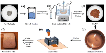 |
| | Fig. 1 The fabrication process of Cu conductive film: (a) dispersing Ag NPs in Cu(OH)2-based growth solution; (b) and (c) synthesizing Cu NPs using a seed-mediated growth method; preparing the (d) conductive adhesive and (e) coated film; (f) obtaining the conductive film after curing. | |
2.5. Preparation of conductive adhesive and film
A conductive adhesive was prepared by mixing 0.7 g of epoxy resin, 0.03 g of 1-cyanoethyl-2-ethyl-4-methylimidazole and 0.6 g of ethanol with Cu NPs, as shown in Fig. 1d. The contents of the as-synthesized Cu NPs in the total mass of the system (excluding ethanol) were 60 wt%, 70 wt%, 80 wt% and 90 wt%, respectively. The mixture was further blended using a high-speed homogenizer. The conductive adhesive was coated onto the polyimide substrates (Fig. 1e), then dried at 210 °C for 10 min under N2 atmosphere to facilitate the evaporation of organic solvent and curing of the resin (Fig. 1f).
2.6. Characterization
The crystal structure of Ag NPs and Cu NPs was analysed using powder X-ray diffraction (PXRD) data. The measurement was conducted on a SmartLab (Rigaku) with Cu Kα radiation (10° ≤ 2θ ≤ 80°, Δ2θ = 0.02°). The morphology of Ag NPs and Cu NPs was examined using scanning electron microscopy (SEM, Thermo Fisher Scientific). Additionally, histograms of the lateral dimension distribution were generated by analysing a certain number of samples based on the scale of the SEM images. Gaussian fitting was applied to the histograms to determine the average size. The elemental distribution of Cu NPs was determined by energy dispersive spectroscopy (EDS) using a field emission electron microscope (ZEISS Sigma 360). Transmission electron microscope (TEM) images and selected-area electron diffraction (SAED) patterns were collected with a JEOL JEM-2100F electron microscope. The UV-vis spectra from 200 to 800 nm were obtained through a Lambda 950 UV spectrophotometer (PerkinElmer). The volume resistance (ρ) of the film was calculated according to eqn (5),| | | ρ = Rs × d × G(d/w) × D(l/w), | (5) |
where Rs was measured at 25 °C by a portable four-probe resistance tester (HPS266X, Changzhou Helpass Electronic Technology Co., Ltd, China). The thickness (d) was measured by a spiral micrometer, l is the length of the square cured film, w is the probe spacing (2 mm), G(d/w) is the thickness correction coefficient, and D(l/w) is the dimension correction coefficient.
3. Results and discussion
3.1. Morphological and structural analysis
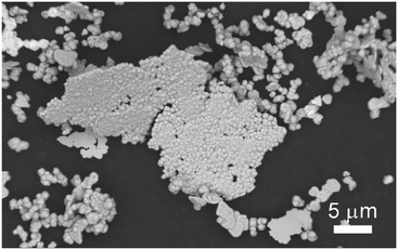
The SEM images and PXRD patterns confirm the successful synthesis of Cu NPs by the typical experiment. After growing copper using Ag NPs as seeds, SEM images, as shown in Fig. 2a and b, reveal a monodisperse plate-like structure with an average lateral dimension of 3.24 μm and a thickness of 410 nm. In addition, a large number of tightly packed small particles can be observed on the surface of the nanoplates. For Ag NPs, the diffraction peaks located at 2θ = 38.1°, 44.2°, 64.4° and 77.3° could be assigned to the (111), (200), (220) and (311) planes of cubic silver (JCPDS: 04-0783) phase, respectively (Fig. 2c). For Cu NPs, the diffraction peaks at 2θ = 43.4°, 50.5° and 74.2° were attributed to the (111), (200) and (220) planes of cubic copper (JCPDS: 04-0836) phase, respectively, and the weak diffraction peaks corresponding to the cubic silver phase were also observed, indicating the coexistence of silver and copper (Fig. 2c). The intensity ratio of ICu(111)/IAg(111) is 24.5, which suggests a higher Cu-to-Ag mass ratio. Furthermore, to study the anisotropic growth of Cu NPs, the texture coefficient (TC) was calculated according to eqn (6).23| | 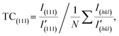 | (6) |
where I(hkl) corresponds to the diffraction peak intensity of the synthesized samples;  comes from standard Ag (JCPDS: 04-0783) and Cu (JCPDS: 04-0836); N is the number of diffraction peaks presented in Fig. 2c. The TC(111) values of Ag NPs and Cu NPs are 3.0 (much greater than 1) and 1.2 (close to 1), respectively, indicating that silver has a preferred orientation of the (111) plane, while copper does not exhibit significant anisotropic growth. Based on the results of SEM and PXRD, the proposed growth mechanism of Cu NPs is shown in Fig. 2d. Copper nucleates at the active sites on the surface of Ag NPs, forming copper nanoparticles. Copper nanoparticles act as new active sites, triggering the formation and aggregation of more copper particles, ultimately forming Cu NPs with silver as the seeds.
 |
| | Fig. 2 (a) and (b) SEM images of Cu NPs; (c) PXRD patterns of Ag NPs and Cu NPs; (d) schematic diagram of the proposed mechanism of Cu NPs. | |
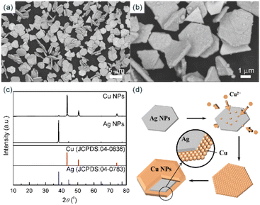
To further elucidate the growth mechanism of Cu NPs, TEM images and SAED patterns were employed. Considering the limited penetration depth of the electron beam, smaller Ag NPs with an average lateral size of 0.61 μm and a thickness of approximately 50 nm were selected as the seeds, and the growth time of Cu NPs was controlled at 10 min. Fig. 3 presents the detailed TEM examination of Cu NPs. Fig. 3a illustrates the two-dimensional morphology of Cu NPs. Fig. 3b and c show the high-resolution TEM (HRTEM) images, in which fringes with lattice spacings of 2.36 and 2.09 Å match the Ag(111) and Cu(111) planes, respectively. The SAED patterns present bright diffraction spots of Ag and Cu. As the unit cell of Ag (4.086 Å) is larger than that of Cu (3.615 Å), the Ag spots should appear closer to the centre spot. As marked in Fig. 3d, the corresponding Ag and Cu spots are aligned on the same line. Moreover, to synthesize Cu NPs under control and investigate the growth mechanism, morphology and size development at various conditions were further studied in detail.
 |
| | Fig. 3 (a) TEM and (b and c) HRTEM images, (d) SAED patterns of Cu NPs. | |
3.2. Influencing factors in the preparation of Cu NPs
3.2.1. The ultrasonic dispersion technique.
The size effect endows nanostructures with high surface energy, making them prone to mutual adsorption and aggregation. The ultrasonic dispersion technique utilizes the mechanical vibration of ultrasonic waves to generate a shear force in the medium. The force induces collisions and shear interactions between particles, thereby promoting effective particle dispersion. Fig. 4 illustrates the morphology of Cu NPs prepared without and with ultrasound, respectively. It can be clearly observed that the ultrasonic dispersion technique significantly alleviates the agglomeration problem of Cu NPs. Therefore, ultrasonic technology was adopted in the subsequent experiments.
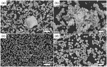 |
| | Fig. 4 SEM images of Cu NPs prepared (a and b) without, and (c and d) with ultrasonic technology. | |
3.2.2. The amount of Ag NPs.
When using the seed-mediated growth method, the amount of seeds is an important factor in the morphology and size of the products. In the blank experiment without using silver seeds, after reacting at 40 °C for 5 h, copper particles with irregular spherical structures were obtained in the Cu(OH)2-based growth solution (Fig. 5a). Moreover, four parallel experiments with different amounts of Ag NPs (mAg = 6, 8, 13 and 25 mg) in 100 mL Cu(OH)2-based growth solution were conducted, while other factors were kept constant (40 °C, 30 min). When mAg was 6 mg, the silvery white colour of Ag NPs was still observed after 30 min of growth. When the growth time was extended to 60 min, all the nanoplates turned reddish brown, indicating that the surface of the nanoplates was completely covered with copper. However, a large number of independent spherical structures were also observed (Fig. 5b), which detached from the surface of Cu NPs to the growth solution due to ultrasonic oscillation. When mAg was increased to 8 mg, Cu NPs with an average lateral dimension of 1.45 μm were obtained after 30 min (Fig. 5f). A large number of densely packed spherical particles can be investigated on the surface of the nanoplates (Fig. 5c). As mAg further increased to 13 mg, the average lateral dimension of Cu NPs increased to 1.95 μm (Fig. 5f), and some aggregates were observed in the SEM images (Fig. 5d). However, as the amount of Ag NPs was increased to 25 mg, the average lateral dimension of the Cu NPs no longer continued to increase, and some aggregates with a size of up to 30 μm appeared (Fig. 5e). The results indicate that the optimal balance between the density of nucleation sites and growth kinetics was achieved when mAg was about 8 to 13 mg. The influence of the Ag NP amount on the size of Cu NPs can be explained by the Avrami theory.24 During the heterogeneous nucleation process, silver seeds provide active sites for nucleation. Once nucleation occurs, the growth process becomes dominant. The increase in seed concentration promotes the nucleation of heterogeneous phases and inhibits their self-growth. The growth of heterogeneous phases is controlled by the diffusion rate of solutes in the growth solution and the growth rate of the nucleus. Therefore, the size of heterogeneous phases does not infinitely increase with the increase of seed concentration. On the contrary, as the seed concentration continues to increase, the active sites for heterogeneous nucleation sharply increase, and the size will correspondingly decrease.
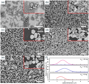 |
| | Fig. 5 SEM images of Cu NPs synthesized (a) without seeds, and with different amounts of Ag NPs: (b) 6 mg, (c) 8 mg, (d) 13 mg, (e) 25 mg, and (f) the corresponding distribution diagram of lateral dimension. | |
3.2.3. The lateral dimension of Ag NPs.
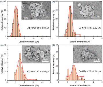
The lateral dimension of silver seeds is another important factor in the morphology of Cu NPs. Herein, the pre-synthesized Ag NPs with average lateral dimensions of 0.55 ± 0.03 μm, 1.18 ± 0.01 μm and 2.44 ± 0.10 μm were used as seeds, respectively, while other conditions were maintained (100 mL growth solution, 40 °C, 30 min). Moreover, it was found that the optimal amount of Ag NPs is related to their lateral dimension. Through a series of comparative experiments, the amount of Ag NPs with three different lateral dimensions was finally determined to be 6, 8 and 25 mg, respectively (Table S1). As shown in Fig. 6, the lateral dimension of the synthesized Cu NPs is obviously larger than that of the corresponding Ag NP seeds. When the lateral dimensions and amount of Ag NPs are relatively small (0.55 μm, 6 mg), the resulting Cu NPs exhibit partial aggregation. It can be considered that the smaller the size of Ag NPs, the larger their specific surface area and surface energy, which makes them more prone to agglomeration between particles.25–27 Furthermore, the behaviour of silver seeds being prone to agglomeration also makes the Cu NPs prone to agglomeration. As the lateral dimension of Ag NPs increases to 1.18 μm, agglomeration of the obtained Cu NPs is alleviated, but the size is not uniform. Further increasing the lateral dimension of Ag NPs to 2.44 μm, the synthesized Cu NPs present good dispersion and high uniformity in size and shape.
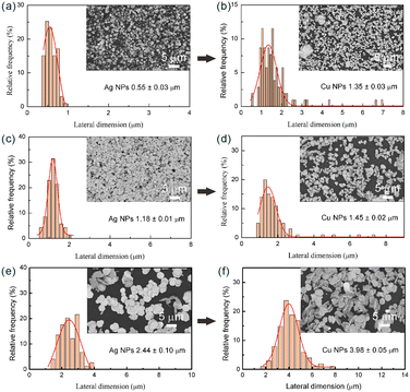 |
| | Fig. 6 SEM images and statistical histograms of the lateral dimension of Ag and Cu NPs. | |
In addition to the morphology, it is also noteworthy that the mass increments of the three synthesized Cu NPs are almost the same, which are 72, 73 and 68 mg, respectively. That is to say, the less silver seeds were used, the higher the proportion of copper ((mCu/(mAg + mCu)) × 100%) in the final product, which has a greater cost advantage in practical applications (Table S1). Therefore, optimizing the aspect ratio of silver seeds could regulate the morphology and size of Cu NPs, and further control their application properties and costs.
3.2.4. The concentration of nickel ions.
The concentration of nickel ions in Cu(OH)2-based growth solution was found to be another factor over the quality of Cu NPs. Fig. 7 shows the SEM images of Cu NPs prepared at various concentrations of nickel ions (0, 5 and 13.3 mM). Without nickel ions in the growth solution, the surface of the synthesized Cu NPs is very rough due to the loose accumulation of a large number of copper particles. When the concentration of nickel ions was adjusted to 5 mM, the copper particles still appeared on the surface of Cu NPs, but their size became smaller. As the concentration of nickel ions increased to 13.3 mM, the surface of Cu NPs became dense and smooth. It was speculated that the nickel ions played two roles in the growth of Cu NPs. On the one hand, the presence of nickel ions reduced the desorption rate of copper from the surface of Cu NPs and enhanced the binding force between particles within the copper layer. On the other hand, the formation of copper–nickel alloy through co-deposition optimized the surface morphology of Cu NPs, creating a dense surface.28,29
 |
| | Fig. 7 SEM images of Cu NPs synthesized under different concentrations of nickel ions in the growth solution: (a) 0, (b) 5 mM, and (c) 13.3 mM. | |
3.2.5. The growth temperature.
Based on the experimental process of synthesizing Cu NPs, 8 mg Ag NPs with an average lateral dimension of 1.18 μm were dispersed in 100 mL Cu(OH)2-based growth solution and reacted for 30 min. The reaction temperature was controlled at 30 °C, 40 °C and 50 °C, respectively. At 30 °C, the colour change of Ag NPs from silvery white to reddish-brown was not observed after 30 min, which suggests that the activity of the growth solution is insufficient to facilitate the reduction of copper at low temperature. By increasing the temperature to 40 °C, Cu NPs with good dispersion, regular morphology, and an average lateral dimension of 1.45 μm were obtained (Fig. 6d). However, when the temperature was increased to 50 °C, the morphology of the product became irregular and uneven. In addition to growing on the surface of the silver seeds, a large number of copper particles adhered to the inner wall of the reaction vessel and fell off into the product in the form of flaky aggregates (Fig. 8). As the growth solution can remain stable for 4 h at 50 °C, the situation in Fig. 8 indicates that the introduction of silver seeds undermined the stability of the growth solution.
 |
| | Fig. 8 SEM image of Cu NPs synthesized at 50 °C. | |
3.2.6. The growth time.
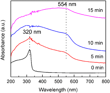
During the growth process at 40 °C, samples were collected at different time intervals of 0, 5, 10, and 15 min. These intervals represent different growth stages of Cu NPs. Fig. 9 presents the UV-vis absorption spectra of the samples at different growth stages. The absorption peak at 320 nm is attributed to the surface plasmon resonance of Ag NPs,30 which gradually weakens and disappears with the extension of growth time, indicating that the silver seeds were coated by copper. The spectra of the samples at time intervals of 5, 10 and 15 min show a broad absorption band centered at 554 nm, which corresponds to the surface plasmon resonance effect of copper.13,31 The peak at 554 nm gradually widens, indicating the growth of Cu NPs.
 |
| | Fig. 9 The UV-vis spectra of Cu NPs at different growth stages. | |
The SEM images (Fig. 10) further demonstrate the growth process of copper on silver seeds. Ag NPs with a lateral dimension of 0.99 μm were selected as the seeds (Fig. 10a). When the growth was carried out for 5 min, the adsorption and growth process of copper ions primarily took place, and the surface of the Ag NPs was gradually coated with a layer of copper nanoparticles (Fig. 10b). Subsequently, with the copper nanoparticles as the core, self-catalytic deposition occurred. After 10 min, a dense copper coating had formed on the surface of Ag NPs, and thereafter, the size of Cu NPs increased substantially (Fig. 10c). As the growth time was extended to 15 min, the lateral dimension of Cu NPs increased to 1.75 μm (Fig. 10d). However, by further extending the growth time, in addition to the plate-like structure, some aggregates were also observed. This phenomenon can be attributed to the gradual decrease in the stability of the growth solution as the reaction time extends. Therefore, simply increasing the reaction time cannot continuously increase the size of Cu NPs.
 |
| | Fig. 10 SEM images and statistical histograms of the lateral dimension of Cu NPs at different growth time intervals: (a) 0 min, (b) 5 min, (c) 10 min and (d) 15 min. | |
3.2.7. The number of growth cycles.
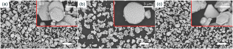
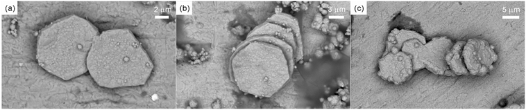
In order to obtain Cu NPs with a larger size and higher copper proportion, a successive growth method was employed. Ag NPs with an average lateral dimension of 6.48 μm and a thickness of 240 nm were used as seeds. The specific process was as follows: three cycles of growth were conducted. After each growth cycle, the obtained Cu NPs were rinsed with deionized water and then dispersed in fresh growth solution, while keeping the growth parameters unchanged. The products from each cycle were collected and investigated. SEM images in Fig. 11a–c illustrate that the size of Cu NPs increases with the number of growth cycles. The aspect ratio of the Cu NPs, determined by dividing the average lateral dimension by the average thickness, decreases progressively from 11.1 to 8.2, and ultimately to 4.0 (Table S2). With the increase in the number of growth cycles, the aspect ratio is expected to continue to decrease, which may eventually lead to the formation of spherical structures. This indicates that as Cu NPs grow, the adsorption process of copper atoms on their surface tends to be isotropic. After each growth cycle, the mass ratio of copper will increase and eventually rise to 88% (Table S2). It is indicated that through the method of successive growth, copper proportion can be gradually increased, thereby controlling the properties and cost of the product.
 |
| | Fig. 11 SEM images of the Cu NPs after successive growth processes: (a) 1st cycle, (b) 2nd cycle, and (c) 3rd cycle. | |
After three growth cycles of the samples, the uniform colour of EDS mapping images (Fig. 12) confirm the homogeneous distribution of Cu, Ni and Ag with the atomic ratio of 100![[thin space (1/6-em)]](https://www.rsc.org/images/entities/char_2009.gif) :1.33:0.14. The detection of silver indicates the presence of silver seeds. The extremely low content indicates that the silver seeds are encapsulated with a large amount of copper, further demonstrating the successful synthesis of copper through seed-mediated growth. The detection of nickel evidences the copper–nickel co-precipitation. Furthermore, a significant spatial heterogeneity of oxygen distribution was observed, with elevated oxygen levels in the background area compared to the surface of Cu NPs. It could be considered that the synthesized Cu NPs behave with excellent metallurgical purity and oxidation resistance, which seems to be closely related to the catalytic activity of the protective interface generated through the co-deposition process.
:1.33:0.14. The detection of silver indicates the presence of silver seeds. The extremely low content indicates that the silver seeds are encapsulated with a large amount of copper, further demonstrating the successful synthesis of copper through seed-mediated growth. The detection of nickel evidences the copper–nickel co-precipitation. Furthermore, a significant spatial heterogeneity of oxygen distribution was observed, with elevated oxygen levels in the background area compared to the surface of Cu NPs. It could be considered that the synthesized Cu NPs behave with excellent metallurgical purity and oxidation resistance, which seems to be closely related to the catalytic activity of the protective interface generated through the co-deposition process.
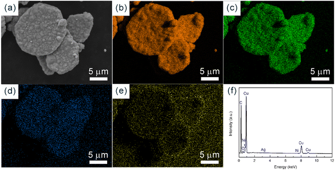 |
| | Fig. 12 (a) SEM image; EDS mapping of (b) Cu, (c) Ni, (d) Ag and (e) O; (f) EDS spectrum of Cu NPs after three growth cycles. | |
3.3. Electrical performance
By selecting the size of silver seeds and adjusting growth conditions, copper plates with different morphologies and sizes can be obtained. The morphology and size of copper plates have significant impact on their electrical properties in practical applications. The electrical properties of three conductive adhesives using different kinds of Cu NPs were studied by testing the resistivity of the conductive films. The copper content was controlled between 60 and 90 wt%, and the average lateral dimensions of Cu NPs were 2.76 (Cu NPs-1), 4.38 (Cu NPs-2) and 8.49 μm (Cu NPs-3), respectively. As shown in Fig. 13, the resistivity of all three films decreases with the increase of copper content, indicating that conductive paths are gradually formed. As the copper content reaches 80 wt%, the decreasing trend of the resistivity slows down, indicating that the resistivity of the films tends to stabilize.
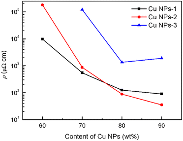 |
| | Fig. 13 The electrical resistivity profiles of Cu NP conductive films. | |
The resistivity of Cu NPs-1 and Cu NPs-2 films is comparable to a certain extent. For Cu NPs-2, the resistivity reaches a minimum value of 35 μΩ cm at a copper content of 90 wt%, which is comparable to experimental conductive pastes and commercial counterparts,20 indicating a potential application in the field of electronic packaging. However, the resistivity of Cu NPs-3 film is significantly higher than that of Cu NPs-1 and Cu NPs-2, which may be due to the loose stacking of conductive networks caused by the large size of the plate-like structure. When the content of Cu NPs-3 exceeds 80 wt%, the resistivity of the coating increases. This is because once the copper content reaches a certain level, it will significantly reduce the fluidity and uniformity of the adhesives, thereby damaging the original conductive network structure. All the results suggest that the contact area of the conductive filler can be increased and the integrity of the conductive network structure can be maintained by optimizing the size of the Cu NPs.
Conclusions
Copper nanoplates were successfully synthesized by a seed-mediated growth method. Pre-synthesized silver nanoplates with different sizes were used as seeds. It has been found that the ultrasonic dispersion technique, the amount and lateral dimension of silver seeds, the concentration of nickel ions, growth temperature and time, as well as the number of growth cycles, are factors affecting the morphology and size of the Cu NPs. By optimizing the growth conditions, Cu NPs with uniform morphology and good dispersion can be prepared in 15 min. Moreover, the aspect ratio of Cu NPs can be regulated by adjusting the growth conditions. The conductive film was fabricated using the developed Cu NP conductive adhesive. The resistivity of the film can be decreased to 35 μΩ cm by increasing the added amount of Cu NPs to 90 wt%. The optimized Cu NPs are considered a promising material for next-generation fine-pitch interconnections in advanced packaging.
Author contributions
Yu Zhou: investigation, visualization, writing – original draft. Ying Liang, Zhen Zhang: formal analysis, writing – review & editing. Shuanglong Yuan: writing – review & editing. Bin Fang: project administration, supervision.
Conflicts of interest
There are no conflicts to declare.
Data availability
All data generated or analyzed during this study are included in this submitted manuscript and its supplementary information (SI).
Supplementary information: the lateral dimension of Ag NPs and the related size and yield of Cu NPs; the variation of yield, aspect ratio, and copper proportion of Cu NPs with growth cycles are included in SI. See DOI: https://doi.org/10.1039/d5ce01031d.
Acknowledgements
We acknowledge the Open Sharing Service Platform for Instruments and Equipment of East China University of Science and Technology for the technical support.
References
- X. Wang, X. Wang, M. Pi and R. Ran, High-strength, highly conductive and woven organic hydrogel fibers for flexible electronics, Chem. Eng. J., 2022, 428, 131172 CrossRef CAS.
- Y. E, Z. Tian, K. Chi, R. Jiang, Y. Lv, Q. Sun and Y. Zhu, Improvement in the thermal conductivity of silver epoxy adhesive by treating with water vapor, Polymers, 2023, 15, 2338 CrossRef CAS PubMed.
- N. Jiang, G. Chen, F. Zhou, B. Ma, C. Zhao and H. Liu, A dual-mode wearable sensor with electrophysiological and pressure sensing for cuffless blood pressure monitoring, J. Mater. Chem. C, 2024, 12, 15915–15923 RSC.
- A. B. M. Tahidul Haque, D. H. Ho, D. Hwang, R. Tutika, C. Lee and M. D. Bartlett, Electrically conductive liquid metal composite adhesives for reversible bonding of soft electronics, Adv. Funct. Mater., 2024, 34, 2304101 CrossRef.
- H. Zhu, X. Hu, B. Liu, Z. Chen and S. Qu, 3D printing of conductive hydrogel−elastomer hybrids for stretchable electronics, ACS Appl. Mater. Interfaces, 2021, 13, 59243–59251 CrossRef CAS.
- Y. Yang, S. Zhong, X. Wang, Y. Gao and X. Cui, Development and applications of mussel-inspired composite hydrogels for flexible bioelectronics, Chem. Eng. J., 2023, 474, 145891 CrossRef CAS.
- C. Zhang, Y. Zhou, H. Han, H. Zheng, W. Xu and Z. Wang, Dopamine-triggered hydrogels with high transparency, self-adhesion, and thermoresponse as skinlike sensors, ACS Nano, 2021, 15, 1785–1794 CrossRef CAS.
- Y. Ji, P. Miao, R. Zhang, Q. Li, Y. Zha, F. Dai, X. Du, B. He and S. Fu, Novel epoxy adhesives based on conductive micron-sized silver flowers, Polym. Compos., 2022, 43, 8761–8770 CrossRef CAS.
- J. Han, J. Yang, W. Gao and H. Bai, Ice-templated, large-area silver nanowire pattern for flexible transparent electrode, Adv. Funct. Mater., 2021, 31, 2010155 CrossRef CAS.
- X. Zhang, Preparation of silver nanopowders and its application in low temperature electrically conductive adhesive, Microelectron. Reliab., 2023, 142, 114917 CrossRef CAS.
- M. R. Sanghvi, O. H. Tambare and A. P. More, Performance of various fillers in adhesives applications: a review, Polym. Bull., 2022, 79, 10491–10553 CrossRef CAS.
- X. Ke, B. Xie, Z. Wang, J. Zhang, J. Wang, Z. Li, H. He and L. Wang, Progress of interconnect materials in the third-generation semiconductor and their low-temperature sintering of copper nanoparticles, Wuji Cailiao Xuebao, 2024, 39, 17–31 CAS.
- Y. Zhang, P. Zhu, G. Li, T. Zhao, X. Fu, R. Sun, F. Zhou and C. Wong, Facile preparation of monodisperse, impurity-free, and antioxidation copper nanoparticles on a large scale for application in conductive ink, ACS Appl. Mater. Interfaces, 2014, 6, 560–567 CrossRef CAS PubMed.
- S. Yokoyama, J. Nozaki, Y. Umemoto, K. Motomiya, T. Itoh and H. Takahashi, Flexible and adhesive sintered Cu nanomaterials on polyimide substrates prepared by combining Cu nanoparticles and nanowires with polyvinylpyrrolidone, Colloids Surf., A, 2021, 625, 126907 CrossRef CAS.
- L. Ma, Z. Lu, Q. Jia, Z. Cui, Y. Wang, D. Li, H. Zhang, G. Zou and F. Guo, Sintering mechanism of bimodal-sized Cu nanoparticle paste for power electronics packaging, J. Electron. Mater., 2024, 53, 2988–2998 CrossRef CAS.
- R. Dang, L. Song, W. Dong, C. Li, X. Zhang, G. Wang and X. Chen, Synthesis and self-assembly of large-area Cu nanosheets and their application as an aqueous conductive ink on flexible electronics, ACS Appl. Mater. Interfaces, 2014, 6, 622–629 CrossRef CAS PubMed.
- S. Li, X. Luo, Z. Sun, H. Zhou, S. Xiong, B. Liu, L. Zeng and B. Yang, Construction of a dual heterogeneous lamella structure to improve the electrical conductivity and mechanical properties of Cu alloys, Mater. Lett., 2023, 338, 134016 CrossRef CAS.
- Y. Noda, S. Yokoyama, T. Itoh and B. Jeyadevan, Formation mechanism of micro-sized Cu plates using Br ions as basal plane-specific adsorbent and their application in the preparation of highly conductive and flexible Cu films, J. Mater. Chem. C, 2024, 12, 15704–15713 RSC.
- M. J. Kim, M. A. Cruz, Z. Chen, H. Xu, M. Brown, K. A. Fichthorn and B. J. Wiley, Isotropic iodide adsorption causes anisotropic growth of copper microplates, Chem. Mater., 2021, 33, 881–891 CrossRef CAS.
- A. Sheng, S. Khuje, J. Yu, T. Parker, J.-Y. Tsai, L. An, Y. Huang, Z. Li, C.-G. Zhuang, L. Kester, Q. Yan and S. Ren, Copper nanoplates for printing flexible high-temperature conductors, ACS Appl. Nano Mater., 2022, 5, 4028–4037 CrossRef CAS.
- H. K. Choi, S. Bae, S.-L. Lee, S. H. Lee, K. Lee, S.-Y. Ko, J.-W. Kang, S.-Y. Yang and T.-W. Kim, Tailoring the internal structure of porous copper film via size-controlled copper nanosheets for electromagnetic interference shielding, Mater. Sci. Eng., B, 2022, 278, 115611 CrossRef.
- H. Gatemala, P. Pienpinijtham, C. Thammacharoen and S. Ekgasit, Rapid fabrication of silver microplates under an oxidative etching environment consisting of O2/Cl−, NH4OH/H2O2, and H2O2, CrystEngComm, 2015, 17, 5530–5537 RSC.
- Z. Zhang, C. Jiang, P. Fu, F. Cai and N. Ma, Microstructure and texture of electrodeposited Ni–ZrC composite coatings investigated by Rietveld XRD line profile analysis, J. Alloys Compd., 2015, 626, 118–123 CrossRef CAS.
- N. Koga, Ozawa's kinetic method for analyzing thermoanalytical curves − history and theoretical fundamentals, J. Therm. Anal. Calorim., 2013, 113, 1527–1541 CrossRef CAS.
- H. Cheng, Z. Yang, F. Du, H. Liu, Q. Zhang and Y. Zhang, Recyclable Ag/halloysite nanotubes/polyvinyl alcohol sponges for enhanced reduction of 4-nitrophenol, Appl. Clay Sci., 2022, 223, 106510 CrossRef CAS.
- S. Mao, F. Pei, S. Feng, Q. Hao, P. Zhang, Z. Tong, X. Mu, W. Lei and B. Liu, Detection of trace Rhodamine B using stable, uniformity, and reusable SERS substrate based on Ag@SiO2-Au nanoparticles, Colloids Surf., A, 2023, 657, 130595 CrossRef CAS.
- H. Reichel, A. García-Valenzuela, J. A. Espino-Román, J. Gil-Rostra, G. F. Regodón, V. Rico-Gavira, A. Borrás, A. Gómez-Ramírez, A. Palmero, A. R. González-Elipe and M. Oliva-Ramírez, Nucleation and growth of plasma sputtered silver nanoparticles under acoustic wave activation, Appl. Surf. Sci., 2024, 669, 160566 CrossRef CAS.
- J.-K. Chang, C.-M. Wu and I.-W. Sun, Nano-architectured Co(OH)2 electrodes constructed using an easily-manipulated electrochemical protocol for high-performance energy storage applications, J. Mater. Chem., 2010, 20, 3729–3735 RSC.
- S. Wang, X. Guo, H. Yang, J. Dai, R. Zhu, J. Gong, L. Peng and W. Ding, Electrodeposition mechanism and characterization of Ni–Cu alloy coatings from a eutectic-based ionic liquid, Appl. Surf. Sci., 2014, 288, 530–536 CrossRef CAS.
- M. Tsuji, S. Gomi, Y. Maeda, M. Matsunaga, S. Hikino, K. Uto, T. Tsuji and H. Kawazumi, Rapid transformation from spherical nanoparticles, nanorods, cubes, or bipyramids to triangular prisms of silver with PVP, citrate, and H2O2, Langmuir, 2012, 28, 8845–8861 CrossRef CAS.
- A. H. Shaik and J. Chakraborty, A simple room temperature fast reduction technique for preparation of a copper nanosheet powder, RSC Adv., 2016, 6, 14952–14957 RSC.
|
| This journal is © The Royal Society of Chemistry 2026 |
Click here to see how this site uses Cookies. View our privacy policy here. 
 *a,
Bin
Fang
a,
Shuanglong
Yuan
*a,
Bin
Fang
a,
Shuanglong
Yuan

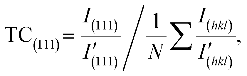
 comes from standard Ag (JCPDS: 04-0783) and Cu (JCPDS: 04-0836); N is the number of diffraction peaks presented in Fig. 2c. The TC(111) values of Ag NPs and Cu NPs are 3.0 (much greater than 1) and 1.2 (close to 1), respectively, indicating that silver has a preferred orientation of the (111) plane, while copper does not exhibit significant anisotropic growth. Based on the results of SEM and PXRD, the proposed growth mechanism of Cu NPs is shown in Fig. 2d. Copper nucleates at the active sites on the surface of Ag NPs, forming copper nanoparticles. Copper nanoparticles act as new active sites, triggering the formation and aggregation of more copper particles, ultimately forming Cu NPs with silver as the seeds.


