Comparative study on substrate quality of laser slicing and wire saw slicing for SiC wafers
Jianfei
Zhang
 ,
Yiyang
Chen
,
Linlin
Che
,
Bixue
Li
,
Xing
Zhang
,
Haoyu
Fan
,
Qingyu
Li
,
Jiawei
Wang
,
YuFeng
Xue
,
Yangyang
Jia
,
Qiu
Chen
*,
Xiufang
Chen
* and
Rongkun
Wang
*
,
Yiyang
Chen
,
Linlin
Che
,
Bixue
Li
,
Xing
Zhang
,
Haoyu
Fan
,
Qingyu
Li
,
Jiawei
Wang
,
YuFeng
Xue
,
Yangyang
Jia
,
Qiu
Chen
*,
Xiufang
Chen
* and
Rongkun
Wang
*
State Key Laboratory of Crystal Materials, Institute of Novel Semiconductors, Shandong University, Jinan 250100, China. E-mail: chenqiu0629@sdu.edu.cn; cxf@sdu.edu.cn; wrk@sdu.edu.cn
First published on 25th November 2025
Abstract
As a representative wide-bandgap semiconductor material, silicon carbide (SiC) is widely used in the fabrication of high-temperature, high-frequency, and high-power devices due to its excellent electronic properties, high thermal conductivity, and extraordinary physicochemical stability. In the manufacturing process of SiC semiconductor devices, substrate slicing serves as a critical link connecting ingots to subsequent processes. For 8-inch SiC ingots, the control difficulty of key parameters—including surface shape accuracy, surface damage, and surface roughness—significantly increases with the enlarged size during slicing. These parameters directly determine the material removal efficiency of subsequent grinding and polishing processes, the global planarization effect of chemical mechanical polishing (CMP), and may even lead to increased defects or device failure if not properly controlled. Therefore, achieving efficient and low-damage slicing of SiC substrates is of great importance. Laser slicing and wire saw slicing are the main processing methods for SiC ingot slicing currently. However, due to the fundamental difference in their processing mechanisms (non-contact vs. contact), the substrate quality resulting from these two methods exhibits significant discrepancies. In this study, 8-inch n-type 4H-SiC ingots were selected as the research object. Characterizations including atomic force microscopy (AFM), high-resolution X-ray diffraction (HR-XRD), scanning electron microscopy (SEM), and Raman spectroscopy were employed to systematically compare the surface shape parameters, crystal integrity, and surface morphology of substrates sliced by the two processes. Furthermore, the evolution law of substrate quality throughout the entire process of “slicing – rough grinding – fine grinding – mechanical polishing (MP) – CMP” was tracked. The research results demonstrate that laser slicing exhibits remarkable advantages over wire saw slicing. This study provides crucial theoretical support and process references for the development of large-scale, low-damage processing technology for third-generation semiconductor substrates.
1. Introduction
Silicon carbide (SiC), a representative of wide-bandgap semiconductor materials, exhibits high critical breakdown electric field, high saturated carrier drift velocity, high thermal conductivity, and excellent physicochemical stability.1,2 Owing to these superior physical and chemical properties, single-crystal SiC is regarded as an ideal semiconductor material for manufacturing optoelectronic devices, high-frequency and high-power devices, and power electronic devices, with wide applications in rail transit, radar and communication, and new energy vehicles.3,4 The preparation and processing of single-crystal SiC substrates are critical links in the manufacturing of SiC devices, directly determining the performance and yield of downstream devices. Therefore, researchers worldwide are committed to scaling up SiC crystals,5 evolving from particle growth to the current 12-inch specification, which is close to the cost-optimal standard. However, SiC is a typical hard-brittle material with low fracture toughness and ultra-high Mohs hardness (∼9.5), leading to easily induced surface damage during SiC wafer processing, high difficulty in controlling shape accuracy, and persistently high processing costs.6Currently, the physical vapor transport (PVT) method is widely adopted in industry to grow bulk single-crystal SiC, followed by a series of processing steps including slicing, grinding, polishing, and cleaning to obtain substrates with atomic-level flatness and no surface damage. Preparing high-quality epitaxial materials on SiC substrates is crucial for improving device performance and reliability, and promoting the application of third-generation semiconductors in production and daily life. In wafer epitaxial growth and device processing, excessive total thickness variation (TTV), Warp, and Bow are undesirable. Wafers with large Warp will induce unwanted stress on the epitaxial film, even causing film cracking and reducing film crystallinity, thereby degrading device performance.7 The current mainstream slicing technologies are laser slicing and wire saw slicing.8
Regarding laser slicing, Kim et al.9 successfully sliced thin SiC from wafers using focused ultrafast double-pulse lasers; the structural changes were caused by the transformation to amorphous SiC and decomposition into amorphous Si and C. The results showed that the kerf loss of the femtosecond laser slicing method was much smaller than that of the traditional wire saw method. Yao et al.10 investigated the effect of different crystal orientations and incident planes on picosecond laser slicing of n-type 4H-SiC, particularly focusing on internal laser ablation lines, cracks, peeling tensile strength, and surface roughness of the peeled surface. The results indicated that the optimal picosecond laser slicing scheme was laser scanning along the [1![[1 with combining macron]](https://www.rsc.org/images/entities/char_0031_0304.gif) 00] orientation from the C-face. Chen et al.11 studied the effect of doping on the picosecond laser absorption characteristics, crack propagation, peeling strength, and surface roughness of the peeled surface. The results showed that increased nitrogen doping concentration led to decreased resistivity and increased laser absorption, which in turn affected the crack propagation length and modified line width. By optimizing processing parameters, high-quality laser slicing of SiC wafers with five gradient doping concentrations was successfully achieved. For wire saw slicing, Hardin et al.12 analyzed the effect of wire feed rate on wafer surface roughness and subsurface damage, and discussed the surface scratch issues caused by loose abrasives and wire stagnation during diamond wire commutation in the cutting process. Li et al.13 used a wire saw with transverse ultrasonic excitation to cut single-crystal SiC workpieces, established kinematic equations for ultrasonic-excited wire saws and conventional wire saws, and analyzed the distinct kinematic characteristics of the two cutting methods. The results showed that compared with conventional diamond abrasive cutting, the diamond abrasive sawing force under ultrasonic excitation was significantly reduced, and the surface morphology of the processed workpiece was smoother. Yang et al.14 used a diamond wire saw to investigate the sawing characteristics and material removal mechanism of polycrystalline SiC ceramics; during the experiment, the wire speed of the diamond wire saw reached 30 m s−1, and the maximum feed rate was 2.0 mm min−1. The results showed that the arithmetic mean surface roughness (Ra) increased slightly with the increase in feed rate.
00] orientation from the C-face. Chen et al.11 studied the effect of doping on the picosecond laser absorption characteristics, crack propagation, peeling strength, and surface roughness of the peeled surface. The results showed that increased nitrogen doping concentration led to decreased resistivity and increased laser absorption, which in turn affected the crack propagation length and modified line width. By optimizing processing parameters, high-quality laser slicing of SiC wafers with five gradient doping concentrations was successfully achieved. For wire saw slicing, Hardin et al.12 analyzed the effect of wire feed rate on wafer surface roughness and subsurface damage, and discussed the surface scratch issues caused by loose abrasives and wire stagnation during diamond wire commutation in the cutting process. Li et al.13 used a wire saw with transverse ultrasonic excitation to cut single-crystal SiC workpieces, established kinematic equations for ultrasonic-excited wire saws and conventional wire saws, and analyzed the distinct kinematic characteristics of the two cutting methods. The results showed that compared with conventional diamond abrasive cutting, the diamond abrasive sawing force under ultrasonic excitation was significantly reduced, and the surface morphology of the processed workpiece was smoother. Yang et al.14 used a diamond wire saw to investigate the sawing characteristics and material removal mechanism of polycrystalline SiC ceramics; during the experiment, the wire speed of the diamond wire saw reached 30 m s−1, and the maximum feed rate was 2.0 mm min−1. The results showed that the arithmetic mean surface roughness (Ra) increased slightly with the increase in feed rate.
The aforementioned studies have made valuable contributions to the advancement of both slicing technologies, laying a foundation for addressing the substrate thinning issue of future electronic devices. However, most studies focus on the optimization of a single slicing technology, lacking systematic comparison of the quality of 8-inch n-type 4H-SiC substrates sliced by the two mainstream processes. In particular, the evolutionary differences in substrate quality throughout the entire process of “slicing – rough grinding – fine grinding – mechanical polishing (MP) – chemical mechanical polishing (CMP)” have not been thoroughly analyzed. Additionally, the mechanism by which the damage types introduced by the two processes (e.g., amorphous layers from laser slicing and microcracks from wire saw slicing) affect the material removal efficiency of subsequent grinding and polishing remains unclear, making it difficult to guide the industry in selecting suitable processing schemes.
Based on this, this study takes 8-inch n-type 4H-SiC ingots as the research object, preparing substrates using laser slicing and wire saw slicing processes respectively, aiming to compare and analyze the different effects of the two slicing processes on substrate quality. Subsequently, the substrates undergo subsequent processing following the “rough grinding – fine grinding – MP – CMP” workflow. Emphasis is placed on comparing the effects of different processes on surface roughness, surface geometry, crystal phase, and stress, revealing the formation mechanism of quality differences during grinding and polishing. Ultimately, this study provides technical support and a theoretical basis for efficient and low-damage processing of 8-inch SiC substrates.
2. Material and experimental methods
2.1 Experimental setup
This study utilized an 8-inch n-type 4° off-axis 4H-SiC ingot grown by the PVT method to systematically conduct a comparative study of laser slicing and wire saw slicing processes, as well as subsequent processing research. Fig. 1(a) presents the schematic diagram of the laser slicing experimental system. A self-developed linearly polarized picosecond laser was employed in the experiment, with its core parameters set as follows: wavelength λ = 1064 nm, pulse width τ ≈ 15 ps, maximum output power of 50 W, and pulse repetition frequency (PRF) ranging from 0 to 500 kHz. After output, the laser was expanded by a beam expander and then transmitted to a liquid crystal spatial light modulator (LC-SLM). The LC-SLM was used to accurately compensate and correct the spherical aberration caused by the different refractive indices of air and 4H-SiC. Subsequently, the laser was focused to a specific depth inside the SiC ingot through a 50× objective lens (numerical aperture NA = 0.65) to form damage points. The processing platform adopts a five-axis motion control system, with a scanning speed adjustable within the range of 0 to 800 mm s−1 and the ability to move along a specific trajectory. A damage layer is formed by connecting points into lines and lines into a surface, followed by ultrasonic treatment at 40 kHz and 200 W for 1 minute to complete the peeling and slicing process. Fig. 1(b) shows the simplified schematic diagram of the wire saw slicing principle. A fixed-abrasive diamond wire saw with irregular tiny diamond particles coated on its surface was used in the experiment. The wire saw moved at high speed and moved relative to the SiC ingot to achieve slicing. To eliminate the interference of uneven composition and defect distribution during the ingot growth process on subsequent quality comparison, a “rotational slicing” scheme was adopted: the 1st wafer was cut by diamond wire saw, the 2nd wafer by the self-developed laser slicing equipment, the 3rd wafer by diamond wire saw, the 4th wafer by laser slicing, and so on. This ensured that the intrinsic properties (e.g., doping concentration, dislocation density) of adjacent wafers were highly similar, providing a fair experimental basis for comparing the quality differences between the two slicing processes. After slicing, all wafers underwent subsequent processing including rough grinding (2000# diamond grinding wheels), fine grinding (8000# diamond grinding wheels), mechanical polishing (∼1 μm diamond slurry), and chemical mechanical polishing (∼200 nm SiO2 slurry). To evaluate process consistency, multiple repeated experiments were conducted under the same processing conditions to avoid accidental random errors. This was conducive to investigating the fluctuations in surface quality, lattice quality, and residual stress distribution, aiming to more accurately compare the differences between laser slicing technology and wire saw slicing technology.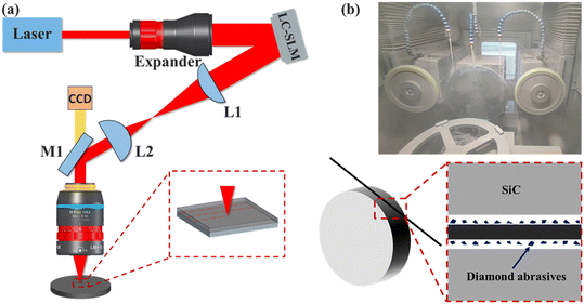 | ||
| Fig. 1 Schematic diagrams of the experimental setups: (a) schematic of the laser slicing system; (b) schematic of the wire saw slicing system. | ||
2.2 Characterization and measurements
To systematically characterize the quality properties of SiC wafers after processing, a multi-dimensional characterization approach was employed to test and analyze their surface morphology, geometric parameters, phase composition, crystal integrity, and internal stress. The specific characterization protocols are as follows: three-dimensional confocal white light interferometric profiler (Sensofar Sneox 090), scanning electron microscope (ZEISS Gemini SEM 560), and atomic force microscope (Park systems NX20) were used to measure surface morphology and roughness. Wafer geometric measurement equipment (Qianshi Intelligent Technology Co., Ltd.) was applied to determine the TTV and Warp of the wafers. Raman confocal microscope (Oxford WITec alpha300R) was utilized for phase analysis and characterization of the wafers. High-resolution X-ray diffractometer (Brucker D8 Discover HR-XRD) was adopted to analyze the lattice distortion induced by processing. Wafer internal stress tester (Strain Viewer 300, Suzhou Ruifei Optoelectronic Technology Co., Ltd.) was used to characterize the overall stress variation of the wafers.3. Material and experimental methods
3.1 Comparison of processing efficiency, loss, and surface state analysis
| Processing time per wafer per min | Material loss per wafer per μm | Number of obtained wafers per pcs | |
|---|---|---|---|
| Laser slicing | 40 | ∼100 | 44 |
| Wire saw slicing | 45 | ∼240 | 33 |
It can be observed that laser slicing technology outperforms multi-wire saw slicing technology in aspects of processing time per wafer, material loss, and number of obtained wafers. In terms of total material loss, multi-wire saw slicing technology is at a disadvantage due to unavoidable kerf loss, resulting in a lower number of obtained wafers compared to laser slicing technology. Regarding processing efficiency, the current laser slicing speed only has a slight advantage, leaving considerable room for improvement. Future research can explore split-beam parallel processing technology and increasing scanning speeds to further enhance laser slicing efficiency. More importantly, laser slicing technology adopts a single-wafer processing method, enabling rapid acquisition of surface quality data (such as surface morphology, TTV, and Warp) of the previous wafer and feedback to the slicing process for iterative improvements.
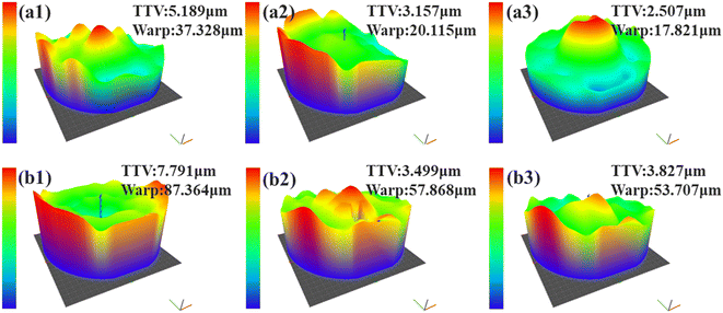
Surface geometric morphology is a crucial evaluation indicator for SiC wafer processing, mainly covering key parameters such as TTV, Warp, and Bow. These parameters directly determine the stability of subsequent processes including epitaxial growth and device fabrication. Excessive Warp may lead to stress concentration or even cracking of the epitaxial film, thereby affecting device performance and reliability. Therefore, this section focuses on analyzing the evolution laws of Warp and TTV of laser-sliced and wire saw-sliced samples under different processing procedures. Fig. 3(a1–a3) shows the 3D surface contour maps of the laser-sliced samples after fine grinding, mechanical polishing (MP), and chemical mechanical polishing (CMP) procedures. As can be seen from the figures, with the advancement of processing procedures, both TTV and Warp of the samples show a decreasing trend: after fine grinding, the TTV is 5.189 μm and the Warp is 37.328 μm; after MP treatment, the TTV decreases to 3.157 μm and the Warp decreases to 20.115 μm; after the CMP procedure, the TTV and Warp reach 2.507 μm and 17.821 μm, respectively. By observing the 3D surface contours of the wire saw-sliced samples in Fig. 3(b1–b3), it can be found that their TTV and Warp also show a gradual decreasing law. This result indicates that the grinding and polishing procedures can not only eliminate the surface/subsurface damage introduced by slicing and release stress through material removal, but also effectively optimize the surface geometric morphology of SiC wafers, laying a foundation for subsequent processes.
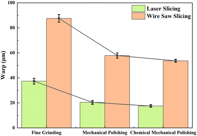
A vertical comparison of the Warp values of the two types of samples under the same grinding and polishing procedures (as shown in Fig. 4) clearly reveals that the Warp values of the laser-sliced samples at each procedure are lower than those of the wire saw-sliced samples. The reason for this difference lies in the principle characteristics of the two slicing processes: wire saw slicing requires fixing the ingot manually or semi-automatically, and then using a high-speed moving diamond wire for contact cutting. During the cutting process, deviations in ingot fixing, wire saw vibration, and other factors are likely to deteriorate the geometric morphology of the wafer. In contrast, laser slicing uses a high-precision laser beam focused on a specific depth inside the ingot, which can accurately control the thickness uniformity of the internal modified layer, resulting in a better initial geometric morphology of the peeled wafer. This advantage not only facilitates the stable implementation of subsequent processes such as epitaxial growth of SiC wafers, but also significantly improves the yield of the device manufacturing production line.
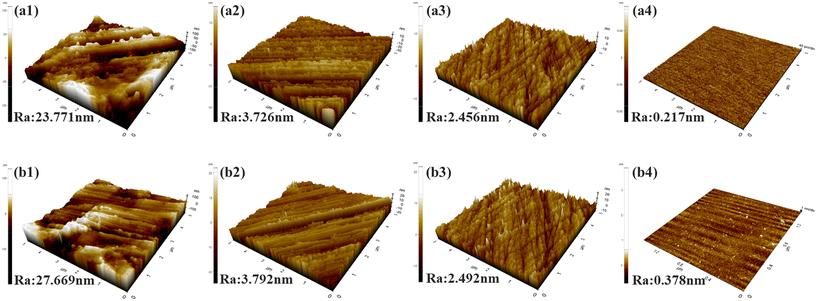
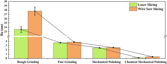
Fig. 5 presents the characterization results of the local surface roughness of laser-sliced and wire saw-sliced samples after rough grinding, fine grinding, MP, and CMP processes, measured by AFM. As shown in Fig. 5(a1–a4), the surface roughness of the laser-sliced samples shows a gradual decreasing trend with the progression of processing procedures: the Ra value is 23.771 nm after rough grinding, decreases to 3.726 nm after fine grinding, further drops to 2.456 nm after MP treatment, and finally reaches 0.217 nm after the CMP process. Observing the roughness variation of the wire saw-sliced samples in Fig. 5(b1–b4), it can be found that they also exhibit a gradual decreasing pattern; however, a vertical comparison of the Ra values of the two types of samples at each processing procedure (as shown in Fig. 6) reveals that the surface roughness of the laser-sliced samples is superior to that of the wire saw-sliced samples in all cases. The core reason for this phenomenon lies in the better total thickness variation (TTV) of the laser-sliced samples: the grinding and polishing processes have high requirements for the wafer's surface shape uniformity. When the overall surface quality of the wafer (such as parameters like TTV and Warp) is better, the abrasive/polishing slurry acts more uniformly during processing, ultimately resulting in better surface quality. Therefore, although the as-sliced surface roughness of the laser-sliced samples is higher than that of the wire saw-sliced samples, relying on the more excellent initial surface shape quality, the subsequent grinding and polishing effects of the laser-sliced samples are better, and finally, the surface roughness of the laser-sliced samples at all processing procedures surpasses that of the wire saw-sliced samples.
3.2 Analysis of lattice quality and stress distribution
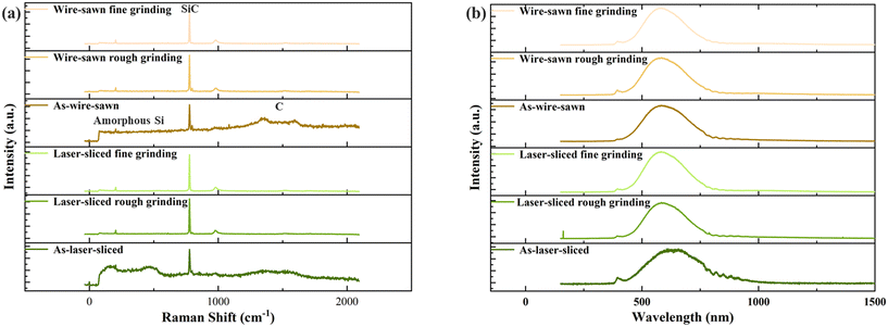 | ||
| Fig. 7 (a) Raman spectroscopy characterization under different processing procedures; (b) photoluminescence spectroscopy characterization under different processing procedures. | ||
After rough grinding of the two types of samples, the characteristic peaks corresponding to amorphous Si and graphite completely disappeared, indicating that the surface phase changes introduced during the slicing process have been basically eliminated; meanwhile, two weak peaks appeared near 200 cm−1 and 980 cm−1, and the signal of the main SiC peak near 780 cm−1 was significantly enhanced. This implies that the amorphous SiC was removed, crystalline SiC began to be exposed, and the ordered arrangement of the SiC lattice was gradually restored. When the two types of samples were further subjected to fine grinding, the sharpness and intensity of the SiC characteristic peaks were further improved, the amorphous layer was completely removed, and the ordered crystalline SiC structure was fully restored. At this point, the Raman spectrum was highly consistent with the spectral characteristics of standard 4H-SiC.20
Fig. 7(b) shows the photoluminescence (PL) spectra of laser-sliced and wire saw-sliced samples at different processing stages. All spectra were normalized based on the maximum intensity of the peaks to clearly compare the relative intensity and peak position characteristics of the PL peaks among different samples. As can be seen from the spectral results, except that the main PL emission peak of the as-laser-sliced sample is located near 640 nm, the main emission peaks of all other samples are concentrated near 575 nm. The essence of this peak position difference is closely related to the correlation between the material's energy level structure and crystal form: the position of the photoluminescence emission peak directly reflects the energy level distribution of the material, and the energy level structure is determined by the microcrystalline form of the crystal.21 Therefore, when there is no significant change in the crystal form, the position of the main PL emission peak usually does not shift with whether the sample is polished or not. Specifically, the peeling surface of the as-laser-sliced sample undergoes obvious distortion in the SiC crystal structure due to the laser action, which further causes a change in the energy level structure and ultimately leads to a significant shift in the position of the main PL emission peak.22 In contrast, all other samples (including wire saw-sliced samples at all stages and laser-sliced samples after grinding and polishing) mainly retain the original crystal form of SiC. The subsequent grinding and polishing processes only improve the surface roughness through material removal and do not have a significant impact on the internal crystal form of the crystal. Thus, the positions of their main PL emission peaks remain basically consistent.
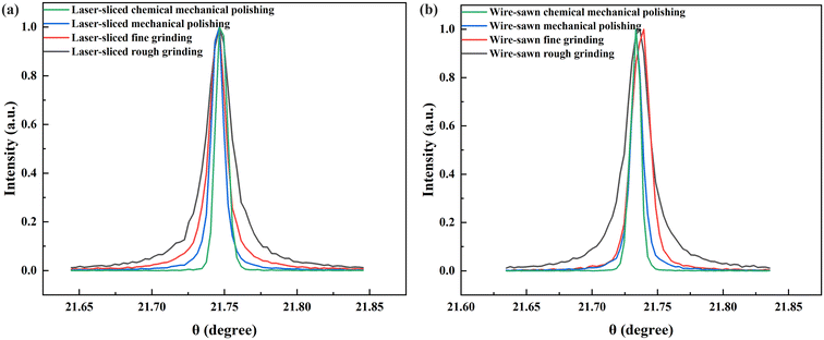 | ||
| Fig. 8 (a and b) Rocking curves of laser-sliced samples and wire saw-sliced samples under different processing steps, respectively. | ||
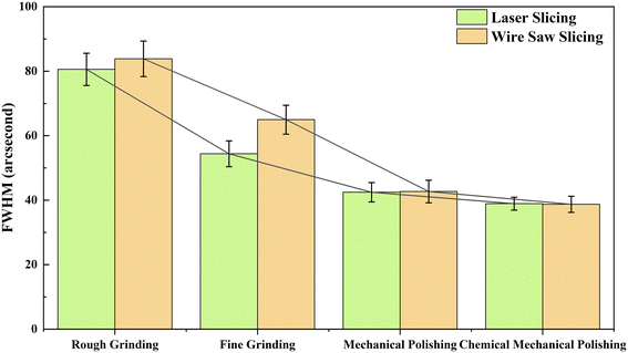
Fig. 8(a) and (b) show the comparison diagrams of XRD rocking curves of laser-sliced and wire saw-sliced wafers after rough grinding, fine grinding, MP, and CMP, respectively. Since the 4H-SiC crystals used in the experiment were grown with a 4° off-angle, the characteristic peak positions of their rocking curves are concentrated around 21.75°.23 From the characteristics of the curves, it can be seen that as the processing precision gradually improves, the FWHM of the rocking curves shows a continuous narrowing trend—which indicates that the crystal quality of the wafers is gradually improved, specifically reflected in the release of residual stress and the enhancement of lattice integrity. The underlying mechanism is as follows: the slicing process will cause lattice distortion near the wafer surface, which in turn broadens the rocking curve; the blurred secondary peaks accompanied in the rocking curve further confirm that severe processing damage has induced the formation of sub-grain structures. With the advancement of grinding, polishing, and other procedures, the surface and subsurface damage is gradually removed, the FWHM narrows accordingly, and the crystal quality is improved synchronously. This result confirms that the FWHM is positively correlated with the degree of wafer surface damage.24
Fig. 9 presents the statistical variation trend diagram of FWHM for multiple groups of laser-sliced and wire saw-sliced samples under different processing procedures. It can be intuitively observed from the data that as the precision processing procedures progress, both types of sliced samples exhibit a consistent evolution law—the FWHM decreases continuously, which further verifies the conclusion that “improved processing precision can enhance crystal quality”. It should be noted that there are phased differences in the FWHM variation between the two types of samples: the FWHM of wire saw-sliced samples after rough grinding and fine grinding is slightly larger than that of laser-sliced samples at the same stage; after the MP and CMP procedures, the FWHM values of the two types of samples tend to be consistent. The core reason for this difference lies in the processing characteristics of wire saw slicing technology: the wire saw slicing process causes deeper surface and subsurface damage to the wafers, resulting in more residual lattice distortion in the first two rough processing procedures, which in turn manifests as a larger FWHM. The subsequent high-precision MP and CMP procedures can completely remove the residual damage of both types of samples, and finally make their FWHM reach the same level.
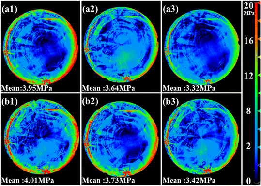
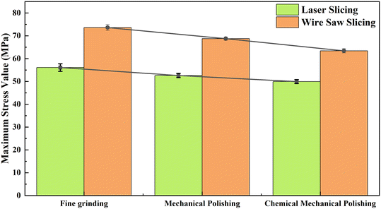
To further quantify the stress difference between the two types of samples, Fig. 11 provides the variation curves of the maximum stress value of the two sliced samples after different grinding and polishing processes. The data shows that the maximum stress value of both types of samples decreases with the progression of processing procedures, and the maximum stress value of the laser-sliced samples is always better than that of the wire saw-sliced samples. The core mechanism of this difference is related to the processing characteristics of the two slicing technologies: during the wire saw slicing process, there is a strong mechanical interaction between the brittle 4H-SiC crystal and the moving metal wire, which easily introduces residual stress inside the wafer.26 Moreover, parameters such as the tension, shape, and feed rate of the metal wire significantly affect the magnitude and distribution of residual stress.27,28 In contrast, laser slicing achieves wafer separation through the internal modified layer cleavage method, which does not require strong mechanical interaction with the crystal and can obtain better surface geometry. Thus, it can effectively reduce residual stress,29 providing a more excellent wafer substrate condition for subsequent device manufacturing.
3.3 Analysis on the interpretation of wafer quality differences
Experimental results and characterization analysis (sections 3.1 and 3.2) indicate that the comprehensive quality of laser-sliced samples is superior to that of wire saw-sliced samples: laser slicing technology not only reduces SiC material loss but also eliminates the need for consumables such as diamond wire saws, minimizes environmental pollution, and significantly improves overall processing efficiency.The differences in processing principles between the two slicing technologies directly lead to obvious distinctions in key indicators such as wafer damage and warpage: the laser slicing process uses an objective lens to precisely focus a high-energy laser beam to a specific depth inside the SiC ingot, forming damage points and local cleavage regions; driven by a translation stage with a positioning accuracy of 1 μm, the ingot moves along a preset path, enabling the construction of a damage layer with uniform depth inside the ingot. Finally, ultrasonic vibration promotes the propagation and connection of cracks to achieve wafer separation.30 In contrast, wire saw slicing requires first fixing the ingot to the cutting chamber via manual or semi-automatic bonding. After manual or semi-automatic alignment, the high-speed moving diamond wire saw is slowly lowered for cutting; during the cutting process, the ingot and diamond wire move in opposite directions, and both plastic grinding zones and brittle fracture zones exist in the cutting area. This phenomenon indicates that external forces cause dislocations and amorphization transitions inside SiC grains, and this process is the core mechanism of material removal during the grinding stage.14 In addition to generating kerf loss equivalent to the wire width, wire saw slicing also leads to large wafer warpage, high material loss, and significantly increased overall stress due to strong mechanical interactions. In particular, when the wafer itself contains inherent defects such as microtubules and dislocations, the internal maximum stress increases further significantly. From the perspective of processing principles and action mechanisms, it can be directly confirmed that wafers prepared by laser slicing are significantly superior to those prepared by wire saw slicing in key substrate parameters such as surface shape accuracy and stress level.
Subsequent processes such as rough grinding, fine grinding, MP, and CMP can effectively optimize the wafer's surface shape accuracy and stress state: regardless of whether the samples are laser-sliced or wire saw-sliced, the comprehensive quality of the wafers is significantly improved after the above-mentioned processes. However, it should be emphasized that laser slicing technology is still far superior to wire saw slicing technology in terms of warpage control. In the semiconductor industry, the epitaxial growth process has extremely high requirements for wafer warpage—wafers with warpage exceeding the standard cannot enter the subsequent processes; the smaller the warpage, the smoother the implementation of subsequent processes such as epitaxy and coating, and the smaller the internal stress of the epitaxial film, which is more conducive to the preparation of high-performance devices. Based on this, future research should focus on the optimization of process parameters for laser slicing technology and the improvement of high-precision automation for wire saw slicing technology, so as to meet the increasingly stringent technical requirements of the semiconductor industry.
4. Conclusion
This study systematically investigated the influence mechanisms of two technologies—laser slicing and wire saw slicing—on the comprehensive quality of 4H-SiC wafers. Multi-dimensional characterization analyses (including surface morphology, lattice quality, and stress state) were conducted to reveal the performance differences between the two slicing technologies. Experimental results indicate that due to the inherent differences in processing principles and methods, laser-sliced samples exhibit significant advantages: first, laser slicing enables wafer separation without physical contact, eliminating the inherent kerf loss of wire saw slicing and thus significantly improving material utilization. Second, laser slicing enables real-time adjustment of process parameters such as focusing depth during processing. Laser-sliced samples outperform wire saw-sliced samples in key parameters such as surface geometry (e.g., flatness, roughness), lattice integrity, and residual stress levels.It is particularly worth noting that the wire saw slicing process has additional technical limitations: on one hand, the cutting process is prone to introducing external contamination, such as electroplated diamond particles detached from the surface of diamond wire saws and impurities carried by the flushing water in the cutting cooling system. On the other hand, if the powder-containing wastewater generated after flushing cutting debris is not properly treated, it may cause potential pollution to the surrounding environment, which is inconsistent with the concept of green manufacturing. After subsequent processes including rough grinding, fine grinding, MP, and CMP, the quality of wafers prepared by both slicing technologies is significantly improved, mainly manifested in the removal of surface damage layers, release of lattice stress, and enhancement of surface shape accuracy. However, comparative analysis shows that the warpage of laser-sliced samples is still significantly better than that of wire saw-sliced samples. The core reason for this difference lies in the inherent distinction between the processing mechanisms and technological characteristics of the two slicing technologies: laser slicing achieves low-damage separation through the internal modified layer cleavage method, while wire saw slicing relies on strong mechanical friction between the diamond wire and the crystal—and this leads to significant differences in the warp control effect.
Beyond the aspects discussed above, laser slicing technology, due to its inherent technical advantages, can be more easily extended to larger-sized (8–12-inch) wafer slicing, whereas multi-wire saw slicing technology is at a disadvantage in this regard. Furthermore, laser slicing adopts a wafer-by-wafer slicing process, allowing for process parameter adjustments both during slicing and after each individual wafer is cut. In contrast, multi-wire saw slicing technology, once initiated, makes subsequent process adjustments difficult.
Based on the above research conclusions, future studies can be carried out from two aspects: first, further optimize the process parameters of laser slicing (e.g., split-beam parallel processing, increasing processing speed, and light field modulation) to achieve wafer separation with higher efficiency, lower damage, and higher precision. Second, improve the technical scheme of wire saw slicing (e.g., develop low-pollution cutting fluid, optimize the diamond wire preparation process, and enhance automatic alignment accuracy) to reduce external contamination and environmental impact. Through the collaborative optimization of the two technologies, the stable preparation of higher-quality SiC wafers will eventually be realized, meeting the stringent requirements of the precision semiconductor industry for high-performance substrate materials.
Conflicts of interest
There are no conflicts to declare.Data availability
The datasets generated during and/or analyzed during the current study are available from the corresponding author upon reasonable request.References
- J. Zhao, P. Ji and Y. Li, et al., Ultrahigh-mobility semiconducting epitaxial graphene on silicon carbide, Nature, 2024, 625(7993), 60–65 CrossRef CAS.
- D. Nakamura, I. Gunjishima and S. Yamaguchi, et al., Ultrahigh-quality silicon carbide single crystals, Nature, 2004, 430(7003), 1009–1012 CrossRef CAS.
- C. R. Eddy and D. K. Gaskill, Silicon Carbide as a Platform for Power Electronics, Science, 2009, 324(5933), 1398–1400 CrossRef CAS.
- G. Wang, D. Sheng and Y. Yang, et al., High-Quality and Wafer-Scale Cubic Silicon Carbide Single Crystals, Energy Environ. Mater., 2024, 7(4), e12678 CrossRef CAS.
- X. Chen, X. Yang and X. Xie, et al., Research progress of large size SiC single crystal materials and devices, Light:Sci. Appl., 2023, 12(1), 28 CrossRef CAS PubMed.
- H. Wu, Wire sawing technology: A state-of-the-art review, Precis. Eng., 2016, 43, 1–9 CrossRef CAS.
- H. Wang, R. Kang and Z. Dong, et al., Ultraprecision machining for single-crystal silicon carbide wafers: State-of-the-art and prospectives, J. Adv. Manuf. Sci. Technol., 2024, 5(2), 2025010 Search PubMed.
- H. Cao, Y. Li and G. Wang, et al., Laser dicing of semiconductor wafers: Research status and current challenges, Opt. Lasers Eng., 2025, 186, 108786 CrossRef.
- E. Kim, Y. Shimotsuma and M. Sakakura, et al., 4H-SiC wafer slicing by using femtosecond laser double-pulses, Opt. Mater. Express, 2017, 7(7), 2450 CrossRef CAS.
- Y. Yao, Q. Chen and B. Li, et al., Influence of crystal orientation and incident plane on n-type 4H-SiC wafer slicing by using picosecond laser, Opt. Laser Technol., 2025, 182, 112174 CrossRef.
- Q. Chen, Y. Yao and J. Zhang, et al., Effect of nitrogen doping concentration on 4H-SiC laser slicing, J. Am. Ceram. Soc., 2025, 108(8), e20555 CrossRef CAS.
- C. W. Hardin, J. Qu and A. J. Shih, Fixed Abrasive Diamond Wire Saw Slicing of Single-Crystal Silicon Carbide Wafers, Mater. Manuf. Processes, 2004, 19(2), 355–367 CrossRef CAS.
- L. Li, S. Yang and B. Du, et al., Study on Processing Process of SiC Single Crystal Cut with Wire Saw Excited by Ultrasonic, 2019 4th International Conference on Mechanical, Control and Computer Engineering (ICMCCE), IEEE, Hohhot, China, 2019, pp. 87–875 Search PubMed.
- H. Yang, M. Fu and X. Zhang, et al., Material Removal Mechanisms of Polycrystalline Silicon Carbide Ceramic Cut by a Diamond Wire Saw, Materials, 2024, 17(17), 4238 CrossRef CAS.
- X. Yu, W. Wu and B. Li, et al., Crack control for efficient nanosecond-laser slicing of large-size 4H-SiC crystals, Appl. Surf. Sci., 2025, 697, 163014 CrossRef CAS.
- H. J. Möller, Basic Mechanisms and Models of Multi-Wire Sawing, Adv. Eng. Mater., 2004, 6(7), 501–513 CrossRef.
- Y. Li, Z. Zhang and Q. Song, et al., Surface micromorphology and nanostructures evolution in hybrid laser processes of slicing and polishing single crystal 4H-SiC, J. Mater. Sci. Technol., 2024, 184, 235–244 CrossRef CAS.
- R. Sugie, Determination of stress components in 4H-SiC power devices via Raman spectroscopy, J. Appl. Phys., 2017, 122(19), 195703 CrossRef.
- Y. Zhang, X. Xie and Y. Huang, et al., Internal modified structure of silicon carbide prepared by ultrafast laser for wafer slicing, Ceram. Int., 2023, 49(3), 5249–5260 CrossRef CAS.
- S. Han, Y. Haijuan and C. He, et al., Laser slicing of 4H-SiC wafers based on picosecond laser-induced micro-explosion via multiphoton processes, Opt. Laser Technol., 2022, 154, 108323 CrossRef CAS.
- M. Na, W. Bahng and H. Jung, et al., Observation of broad triangular Frank-type stacking faults and characterization of stacking faults with emission wavelengths below 430 nm in 4H–SiC epitaxial layers, Appl. Phys. Lett., 2024, 124(15), 152109 CrossRef CAS.
- G. Zhong, S. Ci and Y. Peng, et al., Temperature-dependent photoluminescence spectra mechanism analysis of N–B co-doped 4H–SiC, Mater. Sci. Semicond. Process., 2022, 148, 106767 CrossRef CAS.
- F. Guo, C. Shao and X. Chen, et al., Shape modulation due to sub-surface damage difference on N-type 4H–SiC wafer during lapping and polishing, Mater. Sci. Semicond. Process., 2022, 152, 107124 CrossRef CAS.
- X. Chen, J. Li and D. Ma, et al., Fine machining of large-diameter 6H-SiC wafers, J. Mater. Sci. Technol., 2006, 22(5), 681 CAS.
- C. H. Hsieh, C. Y. Chang and Y. K. Hsiao, et al., Recent Advances In Silicon Carbide Chemical Mechanical Polishing Technologies, Micromachines, 2022, 13(10), 1752 CrossRef.
- Y. Gao and Y. Chen, Sawing stress of SiC single crystal with void defect in diamond wire saw slicing, Int. J. Adv. Manuf. Tech., 2019, 103(1), 1019–1031 CrossRef.
- H. Huang, Y. Zhang and X. Xu, Experimental investigation on the machining characteristics of single-crystal SiC sawing with the fixed diamond wire, Int. J. Adv. Manuf. Tech., 2015, 81(5), 955–965 CrossRef.
- Y. Gao, Y. Chen and P. Ge, et al., Study on the subsurface microcrack damage depth in electroplated diamond wire saw slicing SiC crystal, Ceram. Int., 2018, 44(18), 22927–22934 CrossRef CAS.
- H. Shi, Q. Song and Y. Hou, et al., Investigation of structural transformation and residual stress under single femtosecond laser pulse irradiation of 4H–SiC, Ceram. Int., 2022, 48(17), 24276–24282 CrossRef CAS.
- W. Wu, X. Yu and B. Li, et al., Stress and crack dynamics in nanosecond laser slicing of silicon carbide, Appl. Surf. Sci., 2025, 697, 163052 CrossRef CAS.
| This journal is © The Royal Society of Chemistry 2026 |


