Crown ether-based interface modification for inverted perovskite solar cells with enhanced efficiency and stability
Yang
Zhang
a,
Ting
Jiang
a,
Jingquan
Zhang
 ab,
Lili
Wu
ab,
Guanggen
Zeng
ab,
Lili
Wu
ab,
Guanggen
Zeng
 ab,
Baoyan
Fan
c,
Komiljon
Yakubov
d,
Tulkin
Nurmurodov
 e,
Ilyos
Rakhmatullaev
 f and
Xia
Hao
 *ab
*ab
aInstitute of New Energy and Low-Carbon Technology & College of Materials Science and Engineering, Sichuan University, Chengdu 610065, China. E-mail: hao.xia0808@scu.edu.cn
bEngineering Research Center of Alternative Energy Materials & Devices, Ministry of Education, Chengdu 610065, China
cCollege of Materials and New Energy, Chongqing University of Science and Technology, Chongqing 401331, China
dDepartment of Physics, Urgench State University, Urgench 220100, Uzbekistan
eDepartment of Chemical Technology, Navoi State University of Mining and Technologies, Navoi 210100, Uzbekistan
fDepartment of Mathematics and Physics, Alfraganus University, Tashkent 100190, Uzbekistan
First published on 25th November 2025
Abstract
A crown ether named dibenzo-18-crown-6 is introduced to modify the interface between the perovskite and the electron transport layers. Due to its unique electron cavity and electron-rich system, it effectively passivates defects and simultaneously suppresses cation migration, thereby achieving a high power conversion efficiency of 24.19% with excellent stability.
Organic–inorganic hybrid metal halide perovskites offer great promise as solar-harvesting materials applied in photovoltaics (PV) due to their cost-effective fabrication process, long charge carrier lifetime, tunable band gap, and high absorption coefficient, etc.1–4 Recently, the highest certified PCE of state-of-the-art PSCs has achieved 27.3%.5 According to the deposition sequence of charge transport layers (CTLs), researchers broadly classify PSCs into two main types: normal (n–i–p) and inverted (p–i–n) architectures. Compared to the normal PSCs, inverted PSCs show superior stability, low hysteresis, compatibility with tandem solar cells and competitive PCE, promoting their commercial application.6–9
During the early development of PSCs, however, the efficiency of inverted PSCs always lags behind that of normal PSCs. On the one hand, this observed performance gap could be largely attributed to a large open-circuit voltage (VOC) loss originating from a non-radiative recombination process occurring in the perovskite bulk as well as at the interface within CTLs.10 On the other hand, ion migration, originating from the soft lattice structure of the perovskite, is also an imperative factor that influences the performance of PSCs.11,12 More critically, defects can aggravate ion migration in the perovskite, thus provoking adverse results including material degradation, phase segregation, and interfacial reactions.13,14
Interface regions are more defective than the bulk of perovskite and in particular there are high-density traps on the top surface, resulting from the formation of dangling bonds, which contribute to recombination loss and eventually impede the performance of PSCs.15,16 Therefore, to resolve these problems and achieve efficient and stable inverted PSCs, an interface engineer is pivotal.
In this work, we introduce dibenzo-18-crown-6 (DB18C6) to modify the interface between perovskite and ETL for inverted PSCs. Due to its unique electronegative cavity and electron-rich π bond, DB18C6 could effectively passivate defects, and successfully inhibit ion migration with the assistance of cation-π electrostatic interaction, which strengthens the stability of the devices. In addition, the DB18C6-modification strategy also optimizes the perovskite film, adjusts energy alignment and facilitates charge carrier transport. Leveraging these advantages, the DB18C6-modified PSCs exhibit improved efficiency and stability.
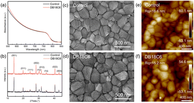
Fig. S1 presents the molecular structure of DB18C6, containing a macrocycle of C–O–C and two benzene rings, with a negatively charged π bond and an electronegative cavity, and thus it can interact with metal cations such as Cs+ and Pb2+ through forming a host–guest complex.17,18 For convenience, we label the untreated perovskites as the control, and the DB18C6-modified perovskites as the target. Ultraviolet-visible (UV-Vis) absorption spectroscopy is employed to investigate the optical properties of the perovskite films with DB18C6-modification. As displayed in Fig. 1a, an enhanced absorbance of the target is observed across the 500–625 nm spectral region, thereby possibly improving the photocurrent of the devices. Additionally, according to the Tauc plot, the Eg of the perovskite can be obtained (Fig. S2), meaning that DB18C6 has no significant impact on the optical properties of the perovskite.
To explore the crystal properties of perovskites, X-ray diffraction (XRD) is conducted (Fig. 1b). It can be seen that both the control and target films display consistent Bragg angles (2θ) without other diffraction peaks appearing, suggesting that the introduction of DB18C6 induces no distinct degradation of the crystal structure of the perovskite. It is worth noting that the target film preferentially enhances the diffraction peak intensities of the (001) and (002) facets, along with observable strengthening of other diffraction peaks. Moreover, after DB18C6 treatment, a noticeable narrowing of full width at half maximum (FWHM) is observed for all principal diffraction peaks in the perovskite films, promoting crystallinity (Table S1).19 Additionally, the mean crystallite size (D) value of the target film (59.93 nm) is larger than 55.94 nm for the control film (Note S1).
The morphology of the perovskite films is researched by scanning electron microscopy (SEM) and atomic force microscopy (AFM). Fig. 1c and d and Fig. S3 reveal that the particle sizes of the perovskite obviously enlarged upon DB18C6-modification, where the average particle sizes are enlarged from 277.9 nm for the control to 307.4 nm for the target films. Similarly, the cross-sectional SEM images reveal non-uniformly enlarged grain size and decreased grain boundaries, which reduces defects and facilitates charge carrier transport (Fig. S4). Furthermore, a lower root-mean-square (RMS) value of 15.2 nm is observed for the target films, compared to 18.6 nm for the control films (Fig. 1e and f). It is identified that DB18C6 can modify surface of perovskites, thus obtaining a more uniform and smoother film. In brief, treatment of DB18C6 promotes crystallization and optimizes interfacial contact, further improving the performance of PSCs.
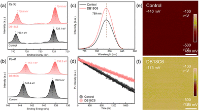
X-ray photoelectron spectroscopy (XPS) is utilized to comprehensively understand the interaction between the perovskite and DB18C6. As displayed in Fig. S5a, a prominent new peak is observed at ∼533.23 eV attributed to O 1s, which is associated with the C–O bond, suggesting the successful absorption of DB18C6 on the perovskite films surface. Concurrently, C 1s spectra reflect enhanced C–O–C bond peak intensity that further verifies the presence of DB18C6 (Fig. S5b).20 Meanwhile, Fig. 2a and b show that both the Cs 3d and Pb 4f peaks shift toward lower binding energies, suggesting that oxygen atoms of DB18C6 form strong Lewis acid-based interactions with Cs+ and Pb2+, further immobilizing cations and passivating uncoordinated Pb2+ defects.21 Moreover, the I 3d core level spectra (Fig. S5c) reveal a peak shift to lower binding energy, probably stemming from anion–π interaction between I− and the benzene ring in DB18C6 or strong coordination between DB18C6 and Pb2+ weakening the Pb–I bond.22,23 Notably, both DB18C6 and PCBM are dissolved in chlorobenzene (CB) during the PSC fabrication. To verify whether DB18C6 could be compromised when PCBM is subsequently spin-coated, we simulate the actual process by treating the DB18C6-modified perovskite film with the same CB solution used for PCBM preparation, followed by the identical spin-coating procedure. As shown in Fig. S6, no significant changes are observed in the C 1s and O 1s spectra of DB18C6 after this treatment–except for a slight decrease in C–O component content (from 37.12% to 30.56%). This result confirms that DB18C6 remains largely intact after exposure to the PCBM–containing CB solution and spin-coating process. Moreover, in terms of Fourier transform infrared spectroscopy (FTIR) results, a slight shift of C–O–C bonds is observed in the range from 1254 and 1130 cm−1 in the pure DB18C6 sample to 1250 and 1128 cm−1 in the target films, implying hydrogen bonding interactions between the perovskite and DB18C6 (Fig. S7).24
 | ||
| Fig. 2 XPS spectra of (a) Cs 3d and (b) Pb 4f of the control and target films. (c) PL and (d) TRPL spectra of the control and target films. KPFM images of the (e) control and (f) target films. | ||
Photoluminescence (PL) and time-resolved photoluminescence (TRPL) are conducted to further study the effect of DB18C6 on the charge dynamics process. As shown in Fig. 2c, relative to the control films, the target films show enhanced luminescence intensity, indicating that DB18C6 effectively suppresses non-radiative recombination loss. According to the TRPL results, a longer lifetime (τave) of 1753.75 ns is observed for the target films compared to 1225.14 ns for the control films (Fig. 2d and Note S2 and Table S2). The passivation effect can be further substantiated by space charge limited current (SCLC) measurements (Fig. S8). The target devices exhibit a lower nt (0.179 × 1016 cm−3) compared to the control devices (0.228 × 1016 cm−3), indicating that the target device has reduced trap density and suppression of Shockley-Read-Hall (SRH) recombination (Note S3).
Kelvin probe force microscopy (KPFM) is used to study how DB18C6 affects electronic properties. As shown in Fig. 2e and f, an increased contact potential difference (CPD) is observed after DB18C6 modification (from −440 mV for the control films to −175 mV for the target films). Meanwhile, in terms of the corresponding CPD statistical chart (Fig. S9), the surface potential distribution of the target film is more concentrated with enhanced intensity, which demonstrates that the post-treatment of DB18C6 is capable of improving the surface potential uniformity of the perovskite film, thereby facilitating favorable contact between the perovskite and ETL. Subsequently, UV photoelectron spectroscopy (UPS) reveals the work function (WF) of 4.30 eV for the control films and 4.25 eV for the target films, supporting the KPFM results (Fig. S10). Additionally, it can also be observed that the energy difference between VBM and WF is 1.31 eV for the control film, which increases to 1.40 eV upon DB18C6-modification. Combining UV-vis data, the energy band structure diagram of the devices is obtained, as shown in Fig. S11. The WF of perovskite is changed because DB18C6 interacts with uncoordinated Pb2+ and Cs+ through Lewis acid–base interaction due to the special electronegative cavity.17 The energy barrier between the perovskite and ETL is then reduced, resulting from the conduction band minimum (CBM) of the perovskite shifting downward by 0.04 eV, thus contributing to optimizing the energy band alignment, prompting charge carrier transport and extraction, and reducing VOC loss.
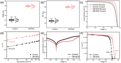
After synthetically investigating the effect of DB18C6-modification on the perovskite, we fabricate inverted PSCs based on a device structure of ITO/NiOx/Me-4PACz/Perovskite/PCBM/BCP/Ag with an optimized DB18C6 concentration of 0.5 mg mL−1 (Fig. S12). The statistical box charts of the main photovoltaic parameters of the device (18 individual devices in each group) are presented in Fig. 3a and b and Fig. S13. These results not only confirm a significant enhancement in device performance upon DB18C6 modification but also demonstrate exceptional experimental reproducibility. Notably, in addition to the improvement in PCE, FF also exhibits an obvious increase, which is ascribed to the interfacial optimization of the perovskite films facilitated by DB18C6, further minimizing resistive losses (Fig. S13c and d). Fig. 3c and Table S3 summarize the current density–voltage (J–V) curves of the corresponding champion devices. The DB18C6-modification device shows a significant enhancement in optoelectronic performance compared to the control device, with PCE of 24.19%, VOC of 1.14 V, FF of 84.15%, and JSC of 25.25 mA cm−2. In addition, a decreased hysteresis index (HI) from 5.99% for the control device to 2.32% for the target device is observed after modification (Note S4 and Table S3). These results demonstrate that DB18C6-modification can serve as a viable approach to construct high-efficiency inverted PSCs, which is attributed to passivation on defects, inhibition of ionic migration and enhanced quality of the perovskite film. Fig. S14 displays the external quantum efficiency (EQE) spectra of two types of PSCs. The target PSCs exhibit higher response within the 650–800 nm wavelength range as well as the corresponding integrated current density.
 | ||
| Fig. 3 (a) Statistical box chart of the PCE and (b) FF, (c) J–V curves, (d) plot of light-dependent VOC, (e) dark J–V curves and (f) C–V curves of the control and target devices. | ||
Aiming to understand the recombination mechanism, we exam the ideal factor (nid) derived from the intensity-dependent VOC tests (Fig. 3d). The nid of the target devices (1.11) is smaller than the control devices (1.23), meaning effective passivation and suppression of trap-assisted recombination (Note S5). We also conduct the J–V measurement in a dark environment (Fig. 3e). The target device shows a significant reduction in dark current near 0 V relative to the control device, indicating reduced electrical leakage channels. Meanwhile, under high forward voltage, its dark current ascends more quickly, indicating better charge transport.25 Afterward, the built-in potential (Vbi) at the top surface is characterized by the capacitance–voltage (C–V) measurement (Fig. 3f). According to Mott Schottky curves, an increase in Vbi from 0.82 V to 0.89 V is observed upon DB18C6-modification, promoting charge separation and transport, thus resulting in a high VOC.
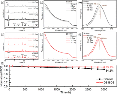
To evaluate the moisture resistance of these perovskite films, we conduct water contact angle tests (Fig. S15). The water contact angle of the control film is 63.3°, whereas the target film exhibits an obviously increased angle of 84.8°. This phenomenon directly demonstrates that DB18C6 prevents water from permeating into the perovskite lattice, which is ascribed to hydrophobic phenyl groups in DB18C6. Furthermore, the SEM images reveal that, after exposure to ambient conditions (25 °C, RH ∼ 45%) for 15 days, the control film initiates degradation at multiple locations; however, the morphology of the target film is still unchanged without degradation (Fig. S16). Moreover, when the samples are continuously exposed under ambient conditions for 35 days, the intensity of each diffraction peak of the control film decreased significantly, especially at 2θ = 14.06°, which relates to the α-phase perovskite peak (Fig. 4a). Notably, a weak diffraction peak appears after 15 days of aging at 2θ = 12.7°, which is characteristic of PbI2 and its intensity gradually increases on aging, meaning severe degradation of the perovskite. By comparison, during the process of aging, there is no striking change in the XRD patterns of the target film except that the diffraction peaks’ intensity decreased slightly (Fig. 4b). In addition, as shown in Fig. 4c and d, with increasing aging time, the UV-Vis spectra of the control film exhibit an obvious red shift and decline in absorbance, whereas a negligible decrease in absorbance is observed in the target film. Similarly, after aging for 35 days, the PL spectrum evolution of the control film reveals emission peak shifts from 789 nm to 794 nm (Fig. 4e), while that of the target film moved only from 789 nm to 790 nm(Fig. 4f). These results conclusively demonstrate that the DB18C6-modification strategy substantially improves the humidity resistance and ambient stability of the perovskite films, benefiting from suppressed ion migration.
Finally, we monitor the PCE evolution process of unencapsulated devices under dark conditions (25 °C, RH ∼ 45%) to assess the long-term reliability of inverted PSCs. After storage for 3000 h, target PSCs demonstrate superior stability, with the PCE retaining 95.1% of its initial value, compared to 84.2% for the control devices (Fig. 4g). We then investigate the operational stability of encapsulated devices through maximum power point tracking (MPPT) in ambient air (20 °C, RH ∼ 45%). As shown in Fig. S17, the target device shows the good stability while maintaining 87.9% of its initial efficiency after 472 h. All in all, benefiting from the defect passivation, inhibition of ion migration and hydrophobic groups of DB18C6, it immensely enhances the long-term stability of inverted PSCs.
In summary, we have developed an interface engineering approach that employs DB18C6 at the top interface, and systematically investigated the modification mechanism. It is observed that DB18C6 can promote crystallization of the perovskite film, passivate defects, inhibit ion migration and adjust the energy level alignment, thereby contributing to substantial improvement in the optoelectronic performance and stability of inverted PSCs. Overall, this work extends the application of crown ethers for efficient and stable inverted PSCs, advancing their commercialization prospects.
The work was financially supported by the National Key Research and Development Program of China (Grant No. 2022YFB4200304), National Natural Science Foundation of China (Grant No. 52202129), the Engineering Featured Team Fund of Sichuan University (No. 2020SCUNG102), the Science and Technology Project of Yibin City (2023JB001) and the Technological Research Program of Chongqing Municipal Education Commission, China (KJQN202301523). The authors gratefully acknowledge Dr Xi Wu from the Analytical & Testing Center of Sichuan University for his help with the component characterization.
Conflicts of interest
There are no conflicts to declare.Data availability
Data will be made available from the corresponding author upon request.The data supporting this article have been included as part of the supplementary information (SI). Supplementary information: materials, device fabrication, measurements, characterizations and notes. See DOI: https://doi.org/10.1039/d5cc05917h.
Notes and references
- M. Yang, Y. Tan, G. Yang, X. Chang, T. Tian, W.-G. Li, Y. Fang, J. Shen, S. Yang and W.-Q. Wu, Angew. Chem., Int. Ed., 2025, 64, e202415966 CrossRef CAS PubMed.
- F. Liu, J. Geng, W. Zhang, J. Dou, Q. Guo, J. Duan and Q. Tang, Chem. Commun., 2024, 60, 11335–11338 RSC.
- Y. Shen, K. Deng, Q. Chen, G. Gao and L. Li, Adv. Mater., 2022, 34, 2200978 CrossRef CAS PubMed.
- K. Chen, H. Lu, Y. Yang, S. Li, K. Jia, F. Wu and L. Zhu, Sol. RRL, 2023, 7, 2200987 CrossRef CAS.
- Martin A. Green, Ewan D. Dunlop, M. Yoshita, N. Kopidakis, K. Bothe, G. Siefer, X. Hao and Jessica Y. Jiang, Prog. Photovoltaics Res. Appl., 2025, 33, 795–810 CrossRef.
- W. Liu, R. Chen, Z. Tan, J. Wang, S. Liu, C. Shi, X. Liu, Y. Cai, F. Ren, Z. Zhou, Q. Zhou, W. Li, T. Miao, H. Zhu, T. Imran, Z. Liu and W. Chen, Adv. Energy Mater., 2025, 15, 2404374 CrossRef CAS.
- W. Peng, K. Mao, F. Cai, H. Meng, Z. Zhu, T. Li, S. Yuan, Z. Xu, X. Feng, J. Xu, M. D. McGehee and J. Xu, Science, 2023, 379, 683–690 CrossRef CAS PubMed.
- X. Zhang, T. Xu, Z. Tian, X. He, S. Zhang, L. Ai, W. Zhang, S. Liu and W. Song, Chem. Commun., 2023, 59, 5874–5877 RSC.
- C. Liu, Y. Yang, H. Chen, J. Xu, A. Liu, A. S. R. Bati, H. Zhu, L. Grater, S. S. Hadke, C. Huang, V. K. Sangwan, T. Cai, D. Shin, L. X. Chen, M. C. Hersam, C. A. Mirkin, B. Chen, M. G. Kanatzidis and E. H. Sargent, Science, 2023, 382, 810–815 CrossRef CAS.
- Q. Jiang and K. Zhu, Nat. Rev. Mater., 2024, 9, 399–419 CrossRef CAS.
- Z. Fang, B. Deng, Y. Jin, L. Yang, L. Chen, Y. Zhong, H. Feng, Y. Yin, K. Liu, Y. Li, J. Zhang, J. Huang, Q. Zeng, H. Wang, X. Yang, J. Yang, C. Tian, L. Xie, Z. Wei and X. Xu, Nat. Commun., 2024, 15, 10554 CrossRef CAS PubMed.
- K. Gao, Y. Fan, D. Liu, Q. Zhao, B. Zhang, C. Gao, X. Zhang, H. Ji, L. Wang and S. Pang, Nano Energy, 2025, 133, 110473 CrossRef CAS.
- Y. Shao, Y. Fang, T. Li, Q. Wang, Q. Dong, Y. Deng, Y. Yuan, H. Wei, M. Wang, A. Gruverman, J. Shield and J. Huang, Energy Environ. Sci., 2016, 9, 1752–1759 RSC.
- K. Niu, C. Wang, J. Zeng, Z. Wang, Y. Liu, L. Wang, C. Li and Y. Jin, J. Phys. Chem. Lett., 2024, 15, 1006–1018 CrossRef CAS PubMed.
- C. Kim, K. Kim, Y. Kim, N. Tsvetkov, N. J. Jeon, B. J. Kang and H. Min, Energy Environ. Sci., 2024, 17, 8582–8592 RSC.
- Z. Ni, C. Bao, Y. Liu, Q. Jiang, W.-Q. Wu, S. Chen, X. Dai, B. Chen, B. Hartweg, Z. Yu, Z. Holman and J. Huang, Science, 2020, 367, 1352–1358 CrossRef CAS PubMed.
- H. Zhang, F. T. Eickemeyer, Z. Zhou, M. Mladenović, F. Jahanbakhshi, L. Merten, A. Hinderhofer, M. A. Hope, O. Ouellette, A. Mishra, P. Ahlawat, D. Ren, T.-S. Su, A. Krishna, Z. Wang, Z. Dong, J. Guo, S. M. Zakeeruddin, F. Schreiber, A. Hagfeldt, L. Emsley, U. Rothlisberger, J. V. Milić and M. Grätzel, Nat. Commun., 2021, 12, 3383 CrossRef CAS PubMed.
- T.-S. Su, F. T. Eickemeyer, M. A. Hope, F. Jahanbakhshi, M. Mladenović, J. Li, Z. Zhou, A. Mishra, J.-H. Yum, D. Ren, A. Krishna, O. Ouellette, T.-C. Wei, H. Zhou, H.-H. Huang, M. D. Mensi, K. Sivula, S. M. Zakeeruddin, J. V. Milić, A. Hagfeldt, U. Rothlisberger, L. Emsley, H. Zhang and M. Grätzel, J. Am. Chem. Soc., 2020, 142, 19980–19991 CrossRef CAS PubMed.
- C. Zhang, X. Shen, M. Chen, Y. Zhao, X. Lin, Z. Qin, Y. Wang and L. Han, Adv. Energy Mater., 2023, 13, 2203250 CrossRef CAS.
- X. Zheng, B. Chen, J. Dai, Y. Fang, Y. Bai, Y. Lin, H. Wei, X. C. Zeng and J. Huang, Nat. Energy, 2017, 2, 17102 CrossRef CAS.
- X. Sun, F. Deng, S. Li, Y. Li, X. Lv, Y.-Z. Zheng and X. Tao, Sol. RRL, 2022, 6, 2200303 CrossRef CAS.
- Z. Huang, Y. Bai, X. Huang, J. Li, Y. Wu, Y. Chen, K. Li, X. Niu, N. Li, G. Liu, Y. Zhang, H. Zai, Q. Chen, T. Lei, L. Wang and H. Zhou, Nature, 2023, 623, 531–537 CrossRef CAS PubMed.
- Y. Cao, X. Zhang, K. Zhao, Y. Wei, L. Zhang, H. Zhang, W. Wang, C. Cui, P. Wang, P. Lin, X. Wu, C. Song, Z. Ni, J. Xue, R. Wang and L. Xu, Adv. Funct. Mater., 2025, 35, 2422205 CrossRef CAS.
- L. Guan, H. Kang, W. Liu and D. Tian, Int. J. Biol. Macromol., 2021, 177, 48–57 CrossRef CAS PubMed.
- Q. Jiang, L. Zhang, H. Wang, X. Yang, J. Meng, H. Liu, Z. Yin, J. Wu, X. Zhang and J. You, Nat. Energy, 2016, 2, 16177 CrossRef.
| This journal is © The Royal Society of Chemistry 2026 |


