Fabrication of a nanowire array surrounded by hexagonally ordered cylindrical walls and structure-enhanced SERS performance
Shengjun
Liu
,
Jizhe
Song
,
Sujuan
Feng
*,
Jiacheng
Li
,
Xiaolong
Wang
,
Xinyue
Wang
,
Dejun
Jiang
and
Guangqiang
Liu
 *
*
School of Physics and Physical Engineering of Qufu Normal University, Qufu 273100, China. E-mail: fengsj@qfnu.edu.cn; gqliu@qfnu.edu.cn
First published on 26th November 2025
Abstract
Conventional reactive ion etching (RIE) treats byproducts as waste contaminants. This study proposes a novel approach to actively utilize zinc-introduced byproducts (ZnF2) for fabricating a nanowire array surrounded by hexagonally ordered cylindrical walls (HOCW-NWA). By harnessing synergistic Au/ZnF2 interactions, this method enables precise nanoarchitecture control. Surface-enhanced Raman spectroscopy (SERS) tests show that the structure achieves a remarkable structural enhancement in the detection performance. This work not only provides a high-performance SERS substrate but also opens a new avenue for turning etching byproducts into functional micro/nanostructures.
Surface-enhanced Raman scattering (SERS) has become a core technology in analytical science, thanks to its single-molecule detection ability and molecular fingerprint recognition characteristics.1–4 However, traditional SERS substrates (such as rough metal surfaces or nanoparticle sol systems) have critical bottlenecks, including strong randomness in the spatial distribution of electromagnetic hotspots, poor signal reproducibility, and insufficient stability, which severely restrict their practical applications. In recent years, nanostructures with precise three-dimensional (3D) periodic arrangements, namely 3D ordered arrays, have attracted significant attention as a new generation of high-performance SERS platforms. Through a precise spatial design, these structures not only achieve precise spatial regulation and intensity homogenization of electromagnetic hotspots, but their unique 3D enhancement volume and photonic crystal effect also significantly improve the sensitivity, reproducibility, and adaptability to complex environments of SERS detection.5–8
Previous studies employed photolithography to fabricate large-area 3D-ordered arrays such as ordered pores, nanotubes, and nanopillars.9–11 Subsequently, the technology expanded to areas including nanoimprinting12 and metal-assisted chemical etching.13 However, these approaches are often limited by high cost and complex procedures. In contrast, the combination of reactive ion etching (RIE) and microsphere masking has emerged as an ideal strategy for constructing high-performance 3D SERS substrates, owing to its efficiency and low cost. This method has already been successfully employed to prepare various high-quality nanostructured materials.14–16
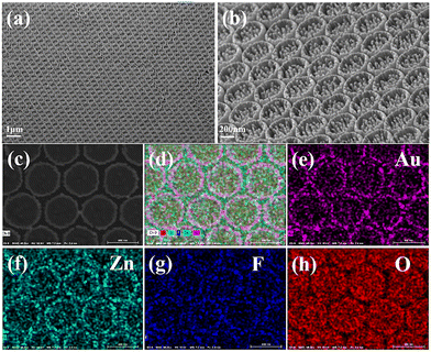
It is noteworthy that conventional RIE fabrication systems based on microsphere masks often regard byproducts in the reaction chamber as interference factors and deliberately remove them to avoid sample contamination. This study innovatively challenges this traditional perception by actively introducing zinc sheets into the RIE reaction chamber, utilizing the byproduct deposition effect to construct a nanowire array surrounded by hexagonally ordered cylindrical walls (HOCW-NWA). As shown in Fig. 1(a) and (b), the structure exhibits a nanowire array surrounded by hexagonally ordered cylindrical walls, with approximately 20 nanowires of 20 nm diameter uniformly distributed within each nanopillar, demonstrating a highly regular periodic arrangement. Energy-dispersive X-ray spectroscopy (EDS) surface elemental analysis was performed on this structure. Fig. 1c presents a front-view scanning electron microscopy (SEM) image of the HOCW-NWA. The elemental mapping (Fig. 1d–h) reveals significant enrichment of zinc and fluorine in the cylindrical wall regions. Nanowire size constraints limited the spatial resolution of Zn/F distribution mapping. However, EDS quantitative analysis revealed a Zn![[thin space (1/6-em)]](https://www.rsc.org/images/entities/char_2009.gif) :
:![[thin space (1/6-em)]](https://www.rsc.org/images/entities/char_2009.gif) F ratio ≈1
F ratio ≈1![[thin space (1/6-em)]](https://www.rsc.org/images/entities/char_2009.gif) :
:![[thin space (1/6-em)]](https://www.rsc.org/images/entities/char_2009.gif) 2 (Table S1), matching ZnF2 stoichiometry. Further X-ray photoelectron spectroscopy (XPS) characterization (Fig. S1) verified the presence of surface ZnF2, providing supplementary validation for the EDS results. Additionally, the detected gold element was primarily distributed on the cylindrical wall surfaces with relatively low content, while the oxygen distribution exhibited high spatial consistency with the silica substrate pillars.
2 (Table S1), matching ZnF2 stoichiometry. Further X-ray photoelectron spectroscopy (XPS) characterization (Fig. S1) verified the presence of surface ZnF2, providing supplementary validation for the EDS results. Additionally, the detected gold element was primarily distributed on the cylindrical wall surfaces with relatively low content, while the oxygen distribution exhibited high spatial consistency with the silica substrate pillars.
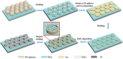
In this experiment, the target structure was fabricated using the RIE technology. The detailed preparation process of HOCW-NWA is described as follows: First, a monolayer of polystyrene (PS) microsphere mask was formed via self-assembly at the gas–liquid interface. Subsequently, the first RIE etching was performed for 100 seconds to create a nanopillar array with PS microspheres covering the top. Next, residual PS microspheres were removed using dichloromethane to obtain nanopillar structures. On this basis, a thin gold film approximately 30 nm thick was deposited on the nanopillar surfaces through magnetron sputtering, thereby preparing a nanopillar array with a metallic surface. Finally, RIE etching was conducted for 140 seconds under the condition of using a zinc sheet. During this process, the gold film fragmented under SF6 plasma bombardment; continuous bombardment led to an increase in substrate temperature, promoting the formation of gold nanoparticles that coated the nanopillar surfaces. As the etching process proceeds, the amount of ZnF2 particles generated in the reaction chamber gradually increases and these particles deposit onto the substrate surface. With a further extension of the etching duration, ZnF2 eventually covers the entire surface of the structure, thus forming the final HOCW-NWA structure, which features a ZnF2 coating as the outer walls, an inner SiO2 nanowire skeleton, and a small amount of Au nanoparticles distributed on the surface. A schematic of the entire fabrication process is shown in Fig. 2, with the corresponding SEM images provided in Fig. S2. This strategy demonstrates excellent structural tunability: by adjusting the diameter of the PS microspheres (e.g., using 1000 nm microspheres), HOCW-NWA structures with different periodic parameters could be conveniently prepared (Fig. S3).
The RIE technique employed in this study involves a dual mechanism combining chemical etching and physical etching. In addition to conventional chemical etching, the radical-induced physical etching process plays a crucial regulatory role in structural construction. Specifically, the high-energy ions generated by fluorine plasma in the radio frequency (RF) electric field exhibit strong sputtering effects, with the sample and sample stage continuously subjected to ion beam bombardment during the etching process. When high-energy particles bombard non-volatile substances in the reaction system, these substances decompose into free-state particles, which diffuse within the reaction chamber and ultimately deposit on the substrate surface. These stable deposits act as highly active sites, inducing further deposition at these locations.17 As the etching process continues, the deposits gradually aggregate, covering the sample surface or forming an etching mask layer.18,19 In our previous research, we successfully fabricated two types of large-scale polystyrene microsphere arrays with ultra-rough surfaces by introducing aluminum sheets into the reaction chamber.20
In this experiment, when a zinc sheet was placed in the chamber, F plasma reacted with Zn during etching, producing ZnF2 on its surface. When etching the planar silica substrate, as mentioned above, the reaction chamber is subjected to a high-frequency electric field environment, where the continuous bombardment of high-energy particles prevents the generated ZnF2 from stably adhering to the zinc surface, dispersing freely within the reaction chamber. As the etching process progresses, ZnF2 particles form nanodots on the substrate surface. These ZnF2 nanodots can be regarded as random micro-etching masks on the substrate surface. Through reactive radical etching of the substrate surface, nanowires with ZnF2 nanodot tips are formed (Fig. S4). During the RIE process, the ZnF2 nanodots are etched, but their etching rate is significantly slower than that of silica. Additionally, throughout the etching process, ZnF2 deposits on the surface, with more deposition occurring on the peaks than in the valleys. EDS spectral analysis further confirmed ZnF2 deposition (Fig. S5).
The introduction of zinc sheets plays a crucial role in the formation of nanowires. To further investigate the formation mechanism of HOCW-NWA, we monitored the entire process (Fig. S6). During the initial stage of RIE etching (50 s), dense nanoparticles were already present on the tops of the gold-plated nanopillars. As the etching time extended to 80 s and 120 s, nanowires began to form under the masking effect of the nanoparticles, while the cylindrical outer walls became delineated. Upon reaching 140 s of etching, the target structure was fully developed: the height of the nanowires increased from approximately 50 nm to about 100 nm, and the cylindrical outer walls grew to around 120 nm, ultimately forming a typical “outer wall-nanowire” composite array structure.
As previously mentioned, the nanodots on the substrate surface can induce the aggregation of deposited materials around them. Likewise, the gold nanoparticles formed on the nanopillar surfaces also enhance the deposition of ZnF2. To verify this effect, we etched nanopillars without a gold coating under the same conditions, resulting in a “nanopillar-with-nanowires” structure (Fig. 3a). The results showed that the nanowire density formed at their tops was significantly lower than that on the HOCW-NWA, and no nanopillar outer wall structure was formed. To further confirm the induction effect of gold nanoparticles on ZnF2 deposition, we conducted etching experiments on gold-coated planar silica substrates under identical conditions (Fig. 3b). The results showed a markedly higher nanowire density on the gold-coated substrate compared to the uncoated one. Notably, the nanowires formed on the gold-coated substrate exhibited significantly rounded tips. The increased adsorption of ZnF2 by gold nanoparticles at these sites leads to enhanced deposition, resulting in a more pronounced curvature at the apex. Additionally, using this fabrication strategy, we have successfully constructed nanowires on other amorphous substrates (e.g., polyimide (PI), photoresist), while the nanostructure could not be reproduced on crystalline silicon/germanium substrates under the same conditions (Fig. S7).
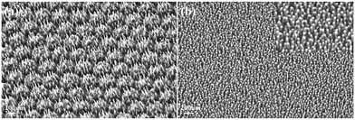 | ||
| Fig. 3 SEM images of the fabricated nanostructures: (a) nanopillar-with-nanowires and (b) nanowires. The inset shows a higher-magnification view. Scale bars are provided. | ||
Leveraging the ability of gold particles to effectively induce ZnF2 deposition, we achieved selective control over nanowire growth regions by regulating the coverage area of the gold film on the nanopillar tops (Fig. 4). Unlike the fabrication process of HOCW-NWA, we utilized the PS spheres on the nanopillar tops as masks for gold film sputtering, followed by the removal of the PS spheres to retain only the edge gold film (Fig. S8). Subsequent etching under the same conditions yielded this structure. Notably, although this structure also consists of a nanowire array surrounded by hexagonally arranged nanopillar outer walls, the spatial distribution of the nanowires exhibits a significant difference: the nanowires are not randomly dispersed within the pillar walls but are highly concentrated at the edge regions (i.e., the gold-coated areas).
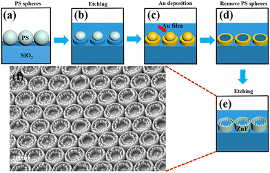 | ||
| Fig. 4 (a)–(e) Schematic illustration of the fabrication process for hexagonal-array nanopillars surrounded by edge nanowires and (f) the corresponding SEM image. | ||
However, in the absence of ZnF2 deposition, smaller-sized gold nanoparticles fail to serve as effective masks for nanowire formation. Control experiments conducted without zinc flakes show that although gold nanoparticles initially cover the cylindrical surface during etching (Fig. S9), they gradually detach from the nanopillar tops as etching progresses. This results in the absence of nanowires at the apex and leads to the formation of a nanocavity-without-nanowire structure. The formation of the outer walls is attributed to the pre-deposited gold layer on the nanopillar sidewalls: this gold layer protects the sidewalls through an ion shielding effect during etching, thereby enabling the formation of the nanopillars’ outer walls under sustained etching. However, due to the lack of ZnF2 deposition, the resulting sidewall height is significantly reduced. Gold film thickness gradient experiments further confirm that the gold film is crucial for constructing complete nanopillar outer walls (Fig. S10). When the gold film thickness falls below 30 nm, incomplete outer wall structures are formed. The integrity of these sidewalls directly affects SERS performance, as discussed in detail later.
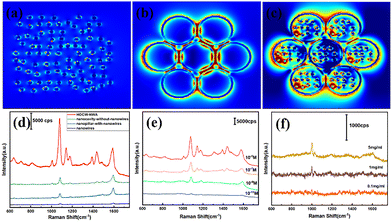
The finite-difference time-domain (FDTD) method was used to simulate the electromagnetic field distribution and elucidate the SERS enhancement mechanism of HOCW-NWAs. As shown in Fig. 5a, the pure nanowire array generated localized surface plasmon resonance hotspots at the wire tips, albeit with a random spatial distribution. For the hexagonal ordered nanocavity structure, hotspots were predominantly concentrated at the cavity edges and the gaps between adjacent cylindrical walls (Fig. 5b). In contrast, the HOCW-NWA integrated both features, retaining the high-intensity gap hotspots while forming additional periodic hotspots with uniform distribution and significantly increased density (Fig. 5c). This optimal field distribution arises from the confinement of plasmonic nanowires within the highly ordered nanocavity units.
The SERS performance of various structures was further systematically compared. Based on the SERS spectra of 10−5 M 4-aminothiophenol (4-ATP) solution (Fig. 5d), the HOCW-NWA demonstrated the most excellent SERS activity. The normalized intensity of its strongest characteristic peak was 6.8-fold, 10.3-fold, and 44.4-fold higher than that of the nanocavity-without-nanowire structure, the nanopillar-with-nanowire structure, and the pure nanowires, respectively. This performance enhancement originated from the synergistic effect of three aspects: (1) the nanocavity “pre-enhanced” the internal optical field via the optical focusing effect; (2) the nanowires, acting as plasmonic antennas, further amplified the local field within the pre-enhanced optical field;21,22 (3) the coupling between hotspots of nanocavities and nanowires might form new hybrid plasmonic modes. Furthermore, the large specific surface area of the nanocavities not only provides more molecular adsorption sites, but their unique structure can also effectively enrich the target molecules to be detected, thereby further enhancing the SERS signal.
Fig. 5e shows the SERS detection results of HOCW-NWAs for 4-ATP at different concentrations. Even at an ultra-low concentration of 10−11 M, the substrate could still identify the characteristic Raman signal at 1075 cm−1. The HOCW-NWA substrate exhibited good signal uniformity (intra-spot RSD ∼4.79%), batch-to-batch reproducibility (RSD ∼18.54%), and stable SERS performance over 30 days of ambient storage (tested on days 1, 10, 20, and 30), as shown in Fig. S11. The influence of the outer walls in HOCW-NWAs on the SERS performance was investigated by examining structures prepared with different gold film thicknesses, as shown in Fig. S12. When the gold film was thinner than 30 nm, the SERS signal was weak due to incomplete outer wall formation. As the thickness exceeded 30 nm, the signal was enhanced and tended to stabilize. Finally, the HOCW-NWA was applied to the detection of real samples: even when the concentration of PS microspheres was as low as 0.1 mg mL−1, clear characteristic peaks were still observed at 1008 cm−1 and 1032 cm−1 (Fig. 5f), demonstrating its high sensitivity for microplastic particle detection. Additionally, the HOCW-NWA substrate exhibits a sensitive response to thiram (Fig. S13).
In summary, this study develops a practical RIE strategy that successfully constructs HOCW-NWA by repurposing ZnF2 etch byproducts into functional building blocks. The resulting architecture uniquely combines the optical focusing effect of nanocavities with the plasmonic enhancement at the nanowire tips, whose synergy endows the material with exceptional SERS sensitivity. This byproduct-repurposing approach is potentially extendable to other metal-halide systems, offering a universal route for the low-cost and scalable fabrication of functional micro/nanostructures. Furthermore, the cavity-tip synergistic enhancement mechanism realized in HOCW-NWA also shows great promise for applications beyond SERS, such as in plasmon-enhanced catalysis and high-sensitivity photodetection.
This work was financially supported by the National Natural Science Foundation of China (Grant No. 52271133).
Conflicts of interest
There are no conflicts to declare.Data availability
The data supporting this article have been included as part of the supplementary information (SI). Supplementary information is available. See DOI: https://doi.org/10.1039/d5cc03525b.Notes and references
- M. Zhao, D. Sikdar, M. Zhao and Y. Ma, Nano Lett., 2025, 25, 8251–8257 CrossRef CAS PubMed.
- H. Zhang, H. Zhang, D. Sikdar, X. Liu, Z. Yang, W. Cheng and Y. Chen, Nano Lett., 2024, 24, 11269–11278 CrossRef CAS.
- X. Yuan, W. Wang, M. Chen, L. Huang, Q. Shuai and L. Ouyang, Chem. Commun., 2024, 60, 8840–8843 RSC.
- R. Xu, L. Tan, Y. Lou, W. Xu, L. Xiao, Y. Zheng and Y. Li, Chem. Commun., 2024, 60, 12872–12875 RSC.
- H. Lu, G. Huang, D. Wang, Q. Ma, Y. Zhang, M. Jin and L. Shui, Chem. Commun., 2025, 61, 1657–1660 RSC.
- Y. Qiu, W. Ding, T. Li, Y. Wang, D. Yang and A. Dong, Chem. Commun., 2024, 60, 9218–9221 RSC.
- G. Li, J. Fan, T. Zhang, T. Gao, Y. Chong, M. Liang, S. Liang, B. Hu, L. Yi, L. Zhao and H. Castel, ACS Sens., 2024, 9, 2031–2042 CrossRef CAS PubMed.
- P. Wen, F. Yang, H. Zhao, S. Li, Y. Xu and L. Chen, ACS Sens., 2024, 9, 6167–6173 CrossRef CAS PubMed.
- A. Mavrokefalos, S. Han, S. Yerci, M. Branham and G. Chen, Nano Lett., 2012, 12, 2792–2796 CrossRef CAS PubMed.
- C. Kim, H. Lee, S. Choi, H. Park and Y. Sohn, Mol. Cryst. Liq. Cryst., 2017, 645, 225–230 CrossRef CAS.
- T. Fujigaya, S. Haraguchi, T. Fukumaru and N. Nakashima, Adv. Mater., 2008, 20, 2151–2155 CrossRef CAS.
- M. Aryal, K. Trivedi and W. Hu, ACS Nano, 2009, 3, 3085–3090 CrossRef CAS PubMed.
- M. Zhang, K. Peng, X. Fan, J. Jie, R. Zhang, S. Lee and N. Wong, J. Phys. Chem. C, 2008, 112, 4444–4450 CrossRef CAS.
- L. Meng, L. Shang, S. Feng, Z. Tang, C. Bi, H. Zhao and G. Liu, Sens. Actuators, B, 2023, 380, 133314 CrossRef CAS.
- S. Liu, J. Song, S. Feng, J. Li, X. Wang, X. Wang, Y. Wang and G. Liu, ACS Appl. Nano Mater., 2025, 8, 9544–9554 CrossRef CAS.
- L. Chang, X. Liu, J. Luo, C. Lee, J. Zhang, X. Fan and W. Zhang, Adv. Mater., 2024, 36, 2310469 CrossRef CAS.
- J. Wu, X. Ye, L. Sun, J. Huang, J. Wen, F. Geng, Y. Zeng, Q. Li, Z. Yi, X. Jiang and K. Zhang, Opt. Express, 2018, 26, 1361–1374 CrossRef CAS PubMed.
- X. Ye, T. Shao, L. Sun, J. Wu, F. Wang, J. He, X. Jiang, W. Wu and W. Zheng, ACS Appl. Mater. Interfaces, 2018, 10, 13851–13859 CrossRef CAS PubMed.
- X. Ye, X. Jiang, J. Huang, F. Geng, L. Sun, X. Zu, W. Wu and W. Zheng, Sci. Rep., 2015, 5, 13023 CrossRef CAS PubMed.
- J. Song, S. Feng, H. Shi, D. Han and G. Liu, Chem. Commun., 2024, 60, 2493–2496 RSC.
- E. Lv, J. Wang, J. Li, X. Zhao, J. Yu, S. Xu, Z. Li, B. Man, M. Xue, J. Xu and C. Zhang, Opt. Express, 2023, 31, 5297–5313 CrossRef CAS PubMed.
- E. Lv, T. Wang, X. Yue, H. Wang, J. Zeng, X. Shu and J. Wang, Chem. Eng. J., 2024, 499, 156020 CrossRef CAS.
| This journal is © The Royal Society of Chemistry 2026 |

