
 Open Access Article
 This Open Access Article is licensed under a
 Creative Commons Attribution 3.0 Unported Licence
Optimized electrical and optical properties of Ag micro-meshes by self-generated cracks for transparent electrodes†
Seung Taek
Jo‡
a,
Jin Wook
Shin‡
a,
Min-Soo
Kim
b,
Sang-Shik
Park
b,
Walter
Commerell
c,
Hyesun
Yoo
 *d,
Jinyoung
Hwang
*e and
Jong Wook
Roh
*ad
*d,
Jinyoung
Hwang
*e and
Jong Wook
Roh
*ad
aDepartment of Hydrogen and Renewable Energy, Kyungpook National University, Daegu 41566, Republic of Korea
bDepartment of Advanced Science and Technology Convergence, Kyungpook National University, Gyeongsangbuk-do 37224, Republic of Korea
cInstitute for Energy and Drive Technology, Technische Hochschule Ulm (THU), 89081, Germany
dRegional Leading Research Center (RLRC) of Smart Energy System, Kyungpook National University, Gyeongsangbuk-do 37224, Republic of Korea. E-mail: vorahsun@gmail.com; jw.roh@knu.ac.kr
eSchool of Electronics and Information Engineering, Korea Aerospace University, Goyang-si, Gyeonggi-do 10540, Republic of Korea. E-mail: jinhwang@kau.ac.ck
First published on 2nd April 2025
Abstract
Transparent conductive electrodes (TCEs) are essential components in the development of various transparent devices. In this study, a Ag micro-mesh network was investigated as an indium-free, non-rigid TCE for applications in flexible devices or solar cells. Instead of a complex and expensive process, such as photolithography with a shadow mask to fabricate a micro-grid, the Ag micro-mesh electrode was fabricated using self-generated cracked templates. The structure of the metallic network was controlled by varying the spin-coating speed and silica solution concentration so that a highly interconnected metallic network can be obtained. Using these techniques, various widths and densities of cracks were obtained and analyzed to compare their optical and electrical properties. Finally, the figure of merit (FoM) for the transparent electrode was calculated based on the measurement results, which revealed that the Ag micro-mesh electrode exhibited the highest performance when the crack widths were mostly distributed in the range of 1–2 μm, regardless of the fabrication conditions. The optimum Ag micro-mesh electrode achieved 88% transmittance at 550 nm wavelength and exhibited 20 Ω sq−1 sheet resistance. These optical and electrical properties are comparable to those of indium-doped tin oxide (ITO) and/or aluminum-doped zinc oxide (AZO) that are used as TCE materials.
Introduction
Transparent conductive electrodes (TCEs) are widely used in various transparent devices, such as touch-screen displays,1,2 solar cells,3,4 smart windows,5,6 and sensors.7,8 Indium-doped tin oxide (ITO) is a representative material for the TCE of most devices because of its excellent optical and electrical properties. Despite its advantages, various alternative materials for ITO have been explored because of the scarcity of indium and the diffusion of metal atoms from ITO into other layers, which induces the degradation of devices.9 Alternative materials for ITO should have high transparency and low sheet resistance as well as the flexibility to be applied in solar cells or devices. Accordingly, various materials, such as metal grids,10,11 silver nanowires (Ag NWs),12,13 carbon nanotubes,14,15 and graphene,16,17 have been extensively studied and have shown good performance as TCEs. However, these materials have limitations regarding their properties and disadvantages. Ag NW-based electrodes have conductivity issues due to the crossbar junctions of NWs; therefore, the Ag NWs must be deposited with a high density, which causes a decrease in the transmittance.14 The applications of carbon nanotubes are limited owing to their high sheet resistance and low stability in air,18 and similarly, graphene has a sheet resistance limitation of 30 Ω sq−1.19 In the case of metal grids, there is no limitation on the properties of the electrode, but a shadow mask is required to proceed with photolithography, rendering it difficult to control the width and density of the metal grid.In contrast to these materials, metal-mesh electrodes are effective candidates to substitute ITO because of the straightforward fabrication process and the use of a removable cracked template to replace the shadow mask. The crack templates are simply fabricated using a dried silica or acrylic solution, which is inexpensive compared with the aforementioned materials. Additionally, the optical and electrical properties of the electrode can be easily controlled by changing the fabrication conditions of the cracked template to rearrange the structure of the metallic networks.20,21 To optimize their performance, metal-mesh electrodes have been extensively investigated to elucidate the formation process of cracks on a solution film and the relationship between crackle patterns and sheet resistances.12,22,23 In addition, metallic networks have outstanding electrical and optical properties, enabling their successful application to flexible devices and solar cells.4,20,24–26
Building on the findings from various studies, an interesting point emerged: nearly all metal-mesh electrodes that demonstrated the best performance had widths predominantly in the 1–2 μm range. This observation led us to hypothesize that the width of the electrode's metallic mesh might play a crucial role in determining its overall performance. As a results, in this study, we focused on investigating the correlation between the width of the micro-mesh grid and the electrode's performance, particularly its figure of merit (FoM). To determine the optimum crack width, we prepared samples with varying crack widths by adjusting the spin-coating speed and colloidal silica concentration, allowing us to systematically evaluate the impact of crack width on the electrode's electrical and optical properties. Additionally, the potential of this Ag micro-mesh was confirmed by applying it to CIGS solar cells.
Experimental
The Ag micro-mesh electrode was fabricated on a glass substrate following the process described in Fig. 1. The soda-lime glass substrate (25 × 25 × 0.7 mm3) was sequentially cleaned with acetone, ethanol, and deionized (DI) water for 30 min each using an ultrasonic cleaner. After the cleaning process, hydrophilic treatment was performed on the surface of the glass to improve adhesion and wettability, which affects the cracking behavior.27 For the hydrophilic treatment, the glass was immersed in a piranha solution composed of sulfuric acid (95 wt%) and hydrogen peroxide (30 wt%) in a ratio of 3![[thin space (1/6-em)]](https://www.rsc.org/images/entities/char_2009.gif) :1 at 75 °C for 2 h. After completing the treatment, colloidal silica (Ludox HS-30, Sigma-Aldrich) was coated on the hydrophilic surface of the glass substrate using a spin coater (WS-400-6NPP-LITE, Laurell). To prepare cracks with various widths and densities, silica solutions with different concentrations were prepared and coated at different spin-coating speeds (2000–6000 rpm) and a spin-coating time of 10 s. Different concentrations of silica solutions were prepared by diluting the colloidal silica to 0.363 g mL−1 (S363) with DI water. Consequently, three different concentrations of colloidal silica, 0.242 (S242), 0.272 (S272), and 0.363 g mL−1 (S363), were prepared to form the crack templates used in this study. The diluted solution, colloidal silica, and DI water were mixed, ultrasonicated for 30 min, and left overnight for stabilization. Before proceeding with the spin-coating process, the diluted and stabilized solution was ultrasonicated again to ensure a uniform concentration. After the spin-coating process, the coated silica film was naturally dried at room temperature at 20–30% relative humidity (RH). As shown in Fig. S1a (ESI†), cracks with silica islands are well developed on the glass substrate, forming a cracked template that can be used to fabricate a micro-mesh structure. Ag thin films, with thicknesses of 80, 120, and 160 nm, were deposited on the cracked template via radio frequency (RF) magnetron sputtering at a power of 30 W. After the sputtering process, the silica islands on the glass were removed via ultrasonic cleaning. Thereafter, the Ag micro-mesh was left on the glass substrate to act as a transparent electrode (Fig. S1b, ESI†). The scanning electron microscopy (SEM) image confirms that the Ag micro-mesh electrodes, with the shape of the silica island, was well fabricated on the glass substrate, as illustrated in Fig. 1. Field-emission scanning electron microscopy (FE-SEM; SU8220, Hitachi) was performed to obtain the surface images and crack widths of the samples. The crack density per sample was calculated based on the literature.28 The detailed calculations are described in Fig. S2 (ESI†). Sheet resistance was measured using a four-point-probe surface resistivity meter (RC2175, EDTM), and transmittance was measured using a spectrophotometer (Spectro 22RS, Labomed) at a wavelength of 550 nm.
:1 at 75 °C for 2 h. After completing the treatment, colloidal silica (Ludox HS-30, Sigma-Aldrich) was coated on the hydrophilic surface of the glass substrate using a spin coater (WS-400-6NPP-LITE, Laurell). To prepare cracks with various widths and densities, silica solutions with different concentrations were prepared and coated at different spin-coating speeds (2000–6000 rpm) and a spin-coating time of 10 s. Different concentrations of silica solutions were prepared by diluting the colloidal silica to 0.363 g mL−1 (S363) with DI water. Consequently, three different concentrations of colloidal silica, 0.242 (S242), 0.272 (S272), and 0.363 g mL−1 (S363), were prepared to form the crack templates used in this study. The diluted solution, colloidal silica, and DI water were mixed, ultrasonicated for 30 min, and left overnight for stabilization. Before proceeding with the spin-coating process, the diluted and stabilized solution was ultrasonicated again to ensure a uniform concentration. After the spin-coating process, the coated silica film was naturally dried at room temperature at 20–30% relative humidity (RH). As shown in Fig. S1a (ESI†), cracks with silica islands are well developed on the glass substrate, forming a cracked template that can be used to fabricate a micro-mesh structure. Ag thin films, with thicknesses of 80, 120, and 160 nm, were deposited on the cracked template via radio frequency (RF) magnetron sputtering at a power of 30 W. After the sputtering process, the silica islands on the glass were removed via ultrasonic cleaning. Thereafter, the Ag micro-mesh was left on the glass substrate to act as a transparent electrode (Fig. S1b, ESI†). The scanning electron microscopy (SEM) image confirms that the Ag micro-mesh electrodes, with the shape of the silica island, was well fabricated on the glass substrate, as illustrated in Fig. 1. Field-emission scanning electron microscopy (FE-SEM; SU8220, Hitachi) was performed to obtain the surface images and crack widths of the samples. The crack density per sample was calculated based on the literature.28 The detailed calculations are described in Fig. S2 (ESI†). Sheet resistance was measured using a four-point-probe surface resistivity meter (RC2175, EDTM), and transmittance was measured using a spectrophotometer (Spectro 22RS, Labomed) at a wavelength of 550 nm.
 | ||
| Fig. 1 Schematic of the fabrication process of the Ag micro-mesh electrode using self-generated cracked templates. | ||
Results and discussion
The SEM images of the S363 samples prepared at different spin-coating speeds are shown in Fig. 2b–f. As the spin-coating speed increased from 2000 to 6000 rpm, the crack widths and silica island size decreased, which indicates an increase in the crack density. The reduction in the silica island size can be identified by observing the dark areas in Fig. 2b–f. As noted in Fig. S1 (ESI†), the dart areas indicate the locations of the silica islands. Lines with a bright gray color in the SEM images signify the Ag micro-mesh electrode that originates from the cracks. Fig. 2 presents that crack density increases as spin-coating speed increases. This phenomenon can be attributed to tensile stress. Previous research29–31 indicates that the crack density increases with decreasing film thickness due to a reduction of tensile stress. In general, a higher spin-coating speed leads to a thinner colloidal silica film, inducing the increase in crack density. Enlarged FE-SEM images of the partial areas in Fig. 2d–f marked in yellow are shown in Fig. 2g–i. Faint lines with thinner crack widths gradually appeared as the spin-coating speed increased from 4000 to 6000 rpm. In Fig. 2b and c, large areas with relatively bright colors are observed, which indicate the detached silica islands during the drying and/or sputtering process; therefore, the Ag thin film was also deposited in these areas. The exfoliated silica islands appear owing to delamination stress from the outside of the liquid region into the wet solid region during the drying process.29 As the crack templates fabricated at 2000 and 3000 rpm are thicker than the others owing to the slower spin-coating speeds,29,30 the silica films coated at 2000 and 3000 rpm were subjected to higher delamination stress, causing the silica islands to be easily detached and/or delaminated. Therefore, the Ag micro-mesh electrode was successfully formed only in the S363 samples coated at 4000–6000 rpm. | ||
| Fig. 2 (a) Crack width distributions of the Ag micro-mesh electrodes fabricated at different spin-coating speeds. FE-SEM images of the S363 samples coated at (b) 2000, (c) 3000, (d) 4000, (e) 5000, and (f) 6000 rpm. Magnified images of the yellow-squared areas in (d)–(f) for the S363 samples coated at (g) 4000, (h) 5000, and (i) 6000 rpm. | ||
To determine the correlation between the crack widths and spin-coating speed, we measured the distribution of the crack widths, as shown in Fig. 2a. The distribution of the crack widths clarified that the average crack widths decreased along with a decrease in the interquartile range, which is represented by the rectangle in Fig. 2a, as the spin-coating speed increased from 2000 to 6000 rpm.
The performances of the Ag micro-mesh electrodes were compared by calculating the FoM for a transparent electrode using the following equation:31,32
 | (1) |
 | ||
| Fig. 3 (a) Transmittance, (b) sheet resistance, and (c) FoM of the transparent electrodes with different thicknesses of the Ag thin film (80, 120, and 160 nm) as a function of the spin-coating speed. | ||
The highest FoM value of 289.7 was obtained for the S363 sample coated at 2000 rpm with an Ag micro-mesh thickness of 80 nm (Fig. 3c). The highest FoM value originates from the detached silica island during the drying and/or sputtering process, so that the deposited area of the Ag thin film is larger than the others, inducing the lowest sheet resistance and transmittance. Hence, the FoM values for the S363 samples coated at 2000 and 3000 rpm (gray-shaded area in Fig. 3c) were not compared with those of the other samples. The silica solution concentration also influences the formation of a crack structure that determines the size of the silica island, crack width, and crack density. The SEM images of the Ag micro-mesh electrodes fabricated at a spin-coating speed of 4000 rpm using different silica solution concentrations of 0.242(S242), 0.272 (S272), and 0.363 g mL−1 (S363) are shown in Fig. 4a–c. The size of the silica islands decreased as the solution concentration decreased from 0.363 to 0.242 g mL−1. Calculating the crack density using a previously reported method,28 the crack density increases from 15.6 (S363) to 47.4 (S242) per 1000 μm, as shown in Fig. S2 (ESI†). Although the crack density increased rapidly, the transmittance improved slightly from 85.6% (S363) to 89.1% (S242), as indicated by the blue line in Fig. 4e. Based on an interquartile range of the boxplot in Fig. 4d, the covered areas of the Ag micro-mesh on the sample surface became similar as the crack widths gradually reduced from 1.14–1.95 μm (S363) to 0.60–0.90 μm (S242). The tendency for the smaller silica island to appear along with the shrinking crack widths as the solution concentration decreases is similar to that reported in the literature.33,34 In contrast to the transmittance, the sheet resistance significantly increases from 15.8 (S363) to 46 Ω sq−1 (S242) as the solution concentration decreased from 0.363 to 0.242 g mL−1. This is because as the crack widths of the Ag micro-mesh decreased, the thickness of the Ag micro-mesh remained the same, which increases the sheet resistance. This phenomenon implies that the crack widths determine the sheet resistance, and low sheet resistances are observed when the crack widths are mainly distributed in the range of 1.14–1.95 μm. Consequently, the FoM value also decreased from 148 (S363) to 69 (S242) owing to the increasing sheet resistance, which reduces the performance of the Ag micro-mesh electrode.
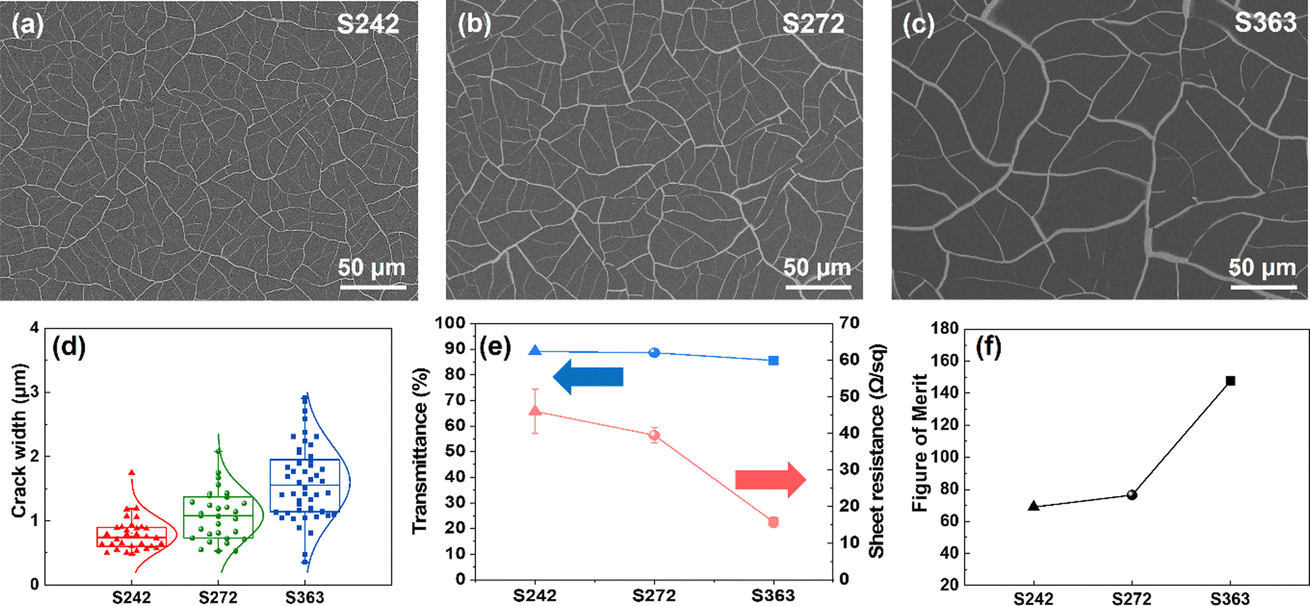 | ||
| Fig. 4 FE-SEM images of the micro-mesh grid obtained using the silica solution concentrations of (a) 0.242 (S242), (b) 0.272 (S272), and (c) 0.363 g mL−1 (S363). (d) Distribution of crack widths, (e) transmittance and sheet resistance, and (f) FoM of the transparent electrodes as a function of the silica solution concentration. | ||
Based on the results in Fig. 3, it is confirmed that the FoM is significantly influenced by the sheet resistance rather than the crack density or transmittance as the transmittance mostly shows similar values in this study. Additionally, in this study, the lowest sheet resistances were obtained when the crack widths were mainly distributed in the range of 1.14–1.95 μm.
To confirm the influence of the crack width on the properties of the Ag micro-mesh electrode, samples with various crack widths were prepared by changing the spin-coating speed from 2000 to 6000 rpm and the solution concentrations from 0.363 to 0.242 g mL−1. The crack widths of all samples are in the range of 0.3–8 μm, as shown in Fig. 5a–c. For the S242 samples coated at 5000 and 6000 rpm (Fig. 5a), cracks were not clearly observed on the silica film. The absence of cracks in these two samples was due to the formation of a silica film thinner than the critical thickness during the spin-coating process, in accordance with the literature data.35,36 The transmittance, sheet resistance, and FoM values of all samples are shown in Fig. 5d–f. The FoM values for the S363 samples coated at 2000 and 3000 rpm and the S272 sample coated at 2000 rpm are excluded in Fig. 5f because the Ag micro-mesh network was unsuccessfully fabricated in these samples, which renders the comparison with other samples difficult. As shown in Fig. S3 (ESI†), the Ag thin film was also deposited in the detached areas of the silica islands in these three samples; therefore, the transmittances of the samples decreased more rapidly in comparison with the others.
 | ||
| Fig. 5 Distributions of the crack width values of (a) S242 (0.242 g mL−1), (b) S272 (0.272 g mL−1), and (c) S363 (0.363 g mL−1) samples as a function of spin-coating speed. (d) Transmittance, (e) sheet resistance, and (f) FoM of the S242, S272, and S363 samples as a function of spin-coating speed. | ||
Similar to the aforementioned results, the FoM values in Fig. 5f considerably depend on the sheet resistance, rather than the transmittance. In particular, the FoM value for the S272 sample decreased almost linearly, whereas the sheet resistance of S272 increased gradually when the spin-coating speed increased from 3000 to 6000 rpm. Notably, the increase in sheet resistance is related to the distribution of the crack widths, in which as the number of crack widths below 1 μm increased, the sheet resistance increased. Fig. 5b shows that the number of crack widths below 1 μm increases with the increase in sheet resistance in Fig. 5e, while the spin-coating speed increased from 3000 to 6000 rpm. When the numbers of crack widths below 1 μm are similar, the sheet resistances are also similar, as shown for the S242 (coated at 4000 rpm) and S272 (coated at 5000 rpm) samples, which have the sheet resistance values of 46 ± 6.04 and 50.3 ± 2.77 Ω sq−1, respectively. Another notable observation is that when the electrode performance was high with a high FoM value, the crack widths were mostly distributed in the range of 1–2 μm. In this study, the S363 sample coated at 4000 rpm (S363_4000 rpm) and the S242 sample coated at 2000 rpm (S242_2000 rpm) exhibited the first and second highest values of FoM at 148 and 142, respectively, as shown in Fig. 5f. Meanwhile, the interquartile ranges of crack widths for the S363_4000 rpm and S242_2000 rpm samples are 1.14–1.96 μm and 0.84–1.67 μm, respectively. Notably, despite the fact that the crack densities of these two samples differ significantly −23.6 per 1000 um for S242_2000 rpm and 15.6 per 1000 um for S363_4000 rpm (a 1.51-fold difference), as described in Fig. S4 (ESI†) – their FoM values remain nearly identical. This suggests that while crack density variations influence both transmittance and Rs, these effects compensate for each other, resulting in a similar overall FoM. Thus, our results indicate that crack width is the dominant factor in determining FoM, rather than crack density.
Fig. 6 clearly indicates that the distribution of crack widths in the samples strongly influence not only the FoM but also the sheet resistance. As shown in Fig. 6, the FoM values can be divided into four sections, which are shaded in different colors, and each section has a similar range of crack width values. The numbers of crack widths indicated by the graphs (Fig. 6(a) and (b)) are designated as the first and third quartile values of the crack width distribution in Fig. 5a–c, which indicate the distribution range of the crack width values in the sample. Furthermore, although the transmittance presents a small difference from 85% to 90%, the sheet resistance significantly changes from 46 to 15.8 Ω sq−1. Meanwhile, the distribution range of the crack width values approaches 1–2 μm (from 0.41–0.69 μm to 0.82–1.95 μm), and the FoM value increases from 40–50 to 140–150. Fig. S4 (ESI†), which describes Fig. 6 in three dimensions, clearly presents the correlation between the FoM, transmittance, and sheet resistance. Based on Fig. S5(a) (ESI†), it is clear that the decrease in the sheet resistance is due to the optimization of the crack widths in the samples, which improves the performance of the Ag micro-mesh electrode. To more clearly illustrate the correlation between crack width and FoM, Fig. 6(c) presents the FoM values of each sample plotted against their average crack width. As clearly shown in Fig. 6(c), the FoM increases gradually as the average crack width increases from a few hundred nm to around 1–2 μm. This result indicates that when the crack width remains below 1 μm, the performance as a transparent electrode significantly degrades. To the best of our knowledge, while the FoM for transparent electrodes has conventionally been studied in relation to the coverage of metallic grids, there have been no clear reports directly correlating FoM with the crack width. Fig. S5(b) (ESI†) presents that the Ag micro-mesh electrodes have a high optical transmittance, revealing that those formed by self-generated cracks can be industrially applied via a simple and low-cost process.
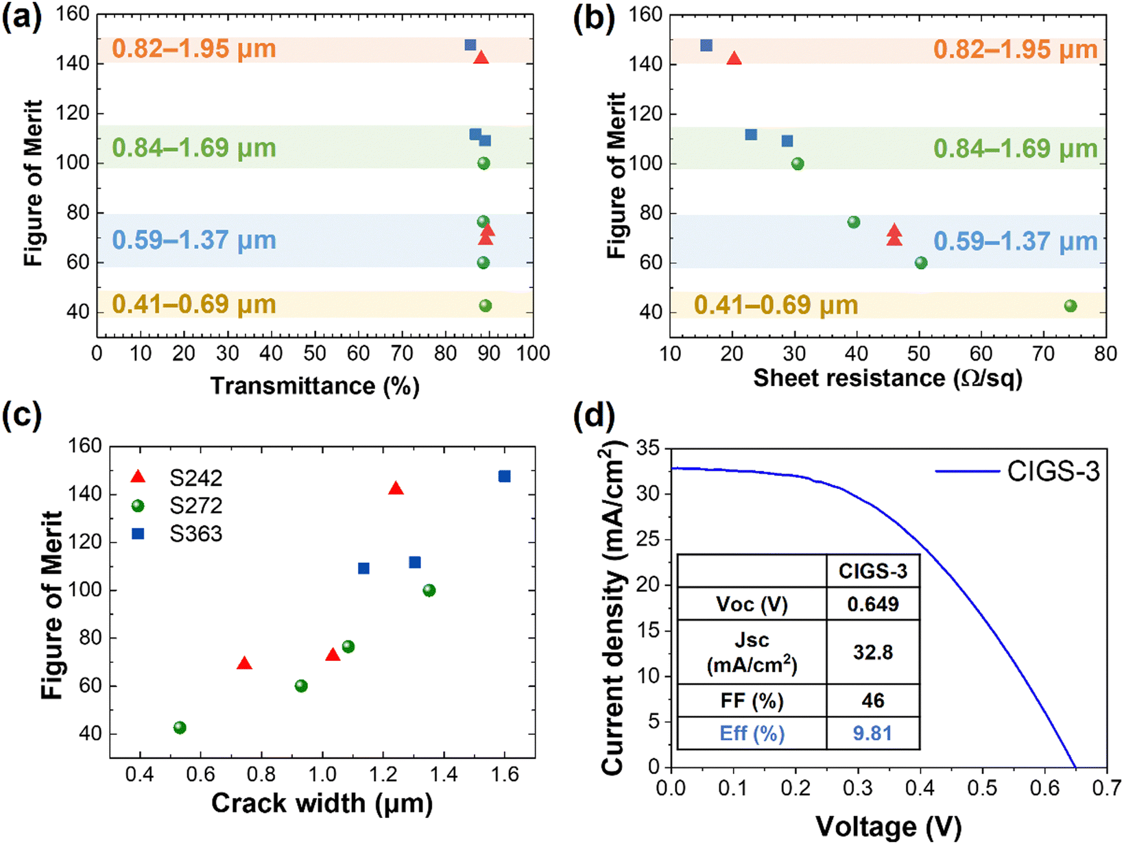 | ||
| Fig. 6 FoM of the Ag micro-mesh electrodes as a function of (a) transmittance, (b) sheet resistance, and (c) average crack width of samples. The numbers stated in the colored areas of (a) and (b) represent the corresponding crack widths of the samples in the same-colored regions. (d) Current density–voltage (J–V) curves of the CIGS solar cell. The inset table provides its solar cell properties. | ||
To evaluate the potential of the Ag micro-mesh network as a functional electrode in devices, it was integrated following the established methods from a previous study.25 The performance of four solar cells, each equipped with the Ag micro-mesh electrode, was analysed by measuring the current density–voltage (J–V) characteristics, as shown in Fig. 6d and Fig. S6, Table S1 (ESI†). These cells achieved power conversion efficiencies ranging from 8.92% to 9.81%. Specifically, the best-performing cell exhibited a short-circuit current density (Jsc) of 32.8 mA cm−2, an open-circuit voltage (Voc) of 0.649 V, and a fill factor (FF) of 46%. These results confirm that the Ag micro-mesh electrode effectively functions as a carrier collector in solar cells, demonstrating its viability as a high-performance electrode in device applications.37
Conclusions
In conclusion, the optimum crack width for the Ag micro-mesh electrode was determined to be approximately 1–2 μm. To verify this, samples with various crack widths were prepared by adjusting the spin-coating speed and silica solution concentration. It was observed that increasing the spin-coating speed led to a more uniform distribution of crack widths, with the average crack width decreasing as the speed increased. Similarly, the silica solution concentration played a significant role in determining crack formation. More diluted solutions resulted in the generation of smaller silica islands, which in turn produced thinner crack widths in the micro-mesh network.One of the most critical findings of this study was the strong correlation between crack width distribution and the sheet resistance. The results showed that as the number of cracks with widths below 1 μm increased, sheet resistance increased substantially. This increase in sheet resistance, however, was not accompanied by a proportional increase in transmittance, which only rose slightly. As a result, the FoM decreased considerably, leading to inferior performance of the Ag micro-mesh electrode. This suggests that the sheet resistance is more sensitive to crack width variations than the transmittance, indicating that maintaining crack widths within a specific range is key to achieving high performance. By clearly demonstrating the correlation between crack width and FoM, this study provides important insights into the optimal width of metallic grids for transparent electrodes, which represents one of the key contributions of this work.
Notably, the highest performance of the Ag micro-mesh electrode, in terms of FoM, was achieved when the crack widths were predominantly distributed in the range of 1–2 μm. In this range, the electrodes exhibited FoM values exceeding 140, regardless of the processing conditions. Specifically, the S363_4000 rpm and S242_2000 rpm samples demonstrated excellent FoM values of 148 and 142, respectively, with transmittance of 88% and 82%, and sheet resistance values of 20 Ω sq−1 and 15 Ω sq−1. These optical and electrical properties are comparable to those of conventional TCEs like ITO, making the Ag micro-mesh electrode a competitive candidate for TCE in various applications. Moreover, applying the Ag micro-mesh network as the metallic electrode on the top layer of a CIGS solar cell resulted in an efficiency of 9.81%, demonstrating the potential of this materials as a high-performance metallic electrode in solar cells.
In summary, the crack width distribution plays a crucial role in determining the electrical and optical properties of the Ag micro-mesh electrode, with the 1–2 μm range proving to be optimal for achieving high FoM values. This work highlights the importance of controlling material microstructure during fabrication to enhance electrode performance, and it opens up new possibilities for the use of Ag micro-mesh electrodes in advanced solar energy technologies.
Author contributions
Seung Taek Jo, Jin Wook Shin: investigation, visualization, writing – original draft. Min-Soo Kim, Sang-Shik Park: resources. Walter Commerell: formal analysis. Hyesun Yoo, Jinyoung Hwang, Jong Wook Roh: supervision, data curation, writing – review & editing, project administration, resources.Data availability
The data supporting this article have been included as part of the ESI.†Conflicts of interest
There are no conflicts to declare.Acknowledgements
This study was supported by the National Research Foundation of Korea (NRF) grant (RS-2021-NR060108, and RS-2023-00249229) funded by the Korean government (MSIT).References
- S. Yuan, Z. Fan, G. Wang, Z. Chai, T. Wang, D. Zhao, A. A. Busnaina and X. Lu, Adv. Sci., 2023, 10, 2304990 Search PubMed.
- J. Sengupta and C. M. Hussain, Nanomaterials, 2022, 12, 3146 CAS.
- S.-H. Lim, H.-J. Seok, M.-J. Kwak, D.-H. Choi, S.-K. Kim, D.-H. Kim and H.-K. Kim, Nano Energy, 2021, 82, 105703 Search PubMed.
- C. P. Muzzillo, M. O. Reese and L. M. Mansfield, ACS Appl. Mater. Interfaces, 2020, 12, 25895–25902 Search PubMed.
- S. Kumar, D. Kang, V. H. Nguyen, N. Nasir, H. Hong, M. Kim, D. C. Nguyen, Y. Lee, N. Lee and Y. Seo, ACS Appl. Mater. Interfaces, 2021, 13, 40976–40985 Search PubMed.
- S. C. Karumuthil, M. K. Ganesha, I. Mondal, A. K. Singh and G. U. Kulkarni, J. Mater. Chem. A, 2022, 10, 23265–23273 RSC.
- Q. Liu, Z. Liu, C. Li, K. Xie, P. Zhu, B. Shao, J. Zhang, J. Yang, J. Zhang and Q. Wang, Adv. Sci., 2020, 7, 2000348 CrossRef CAS.
- I. Mondal, M. K. Ganesha, A. K. Singh and G. U. Kulkarni, Mater. Lett., 2022, 312, 131724 CrossRef CAS.
- T.-H. Han, S.-H. Jeong, Y. Lee, H.-K. Seo, S.-J. Kwon, M.-H. Park and T.-W. Lee, J. Inf. Disp., 2015, 16, 71–84 Search PubMed.
- Z. Chen, R. T. Yin, S. N. Obaid, J. Tian, S. W. Chen, A. N. Miniovich, N. Boyajian, I. R. Efimov and L. Lu, Adv. Mater. Technol., 2020, 5, 2000322 CrossRef CAS PubMed.
- Z. Fakharan and A. Dabirian, Curr. Appl. Phys., 2021, 31, 105–121 CrossRef.
- A. Kim, Y. Won, K. Woo, S. Jeong and J. Moon, Adv. Funct. Mater., 2014, 24, 2462–2471 CrossRef CAS.
- D.-S. Um, Y. Lee, T. Kim, S. Lim, H. Lee, M. Ha, Z. Khan, S. Kang, M. P. Kim and J. Y. Kim, ACS Appl. Mater. Interfaces, 2020, 12, 32154–32162 CrossRef CAS PubMed.
- A. A. Green and M. C. Hersam, Nano Lett., 2008, 8, 1417–1422 Search PubMed.
- D. A. Ilatovskii, E. P. Gilshtein, O. E. Glukhova and A. G. Nasibulin, Adv. Sci., 2022, 9, 2201673 CrossRef CAS PubMed.
- J. Miao and T. Fan, Carbon, 2023, 202, 495–527 CrossRef CAS.
- M. Zarei, M. Li, E. E. Medvedeva, S. Sharma, J. Kim, Z. Shao, S. B. Walker, M. LeMieux, Q. Liu and P. W. Leu, ACS Appl. Mater. Interfaces, 2024, 16, 6382–6393 CrossRef CAS.
- A. Khan, S. Lee, T. Jang, Z. Xiong, C. Zhang, J. Tang, L. J. Guo and W.-D. Li, Small, 2016, 12, 3021–3030 CrossRef CAS PubMed.
- S. Bae, H. Kim, Y. Lee, X. Xu, J.-S. Park, Y. Zheng, J. Balakrishnan, T. Lei, H. Ri Kim and Y. I. Song, Nat. Nanotechnol., 2010, 5, 574–578 CrossRef CAS PubMed.
- B. Han, K. Pei, Y. Huang, X. Zhang, Q. Rong, Q. Lin, Y. Guo, T. Sun, C. Guo and D. Carnahan, Adv. Mater., 2014, 26, 873–877 CrossRef CAS PubMed.
- A. S. Voronin, Y. V. Fadeev, M. O. Makeev, P. A. Mikhalev, A. S. Osipkov, A. S. Provatorov, D. S. Ryzhenko, G. Y. Yurkov, M. M. Simunin and D. V. Karpova, Materials, 2022, 15, 1449 CrossRef CAS PubMed.
- P. B. Catrysse and S. Fan, Nano Lett., 2010, 10, 2944–2949 CrossRef CAS.
- S.-T. Jo, J. W. Shin, W. Commerell, D.-H. Yoo, H. Yoo, J. Hwang, H.-S. Kim, S. Kim and J. W. Roh, Korean J. Met. Mater., 2024, 62, 464–471 CrossRef CAS.
- K. D. M. Rao, C. Hunger, R. Gupta, G. U. Kulkarni and M. Thelakkat, Phys. Chem. Chem. Phys., 2014, 16, 15107–15110 Search PubMed.
- H. Yoo, H. Van Quy, I. Lee, S. T. Jo, T. E. Hong, J. Kim, D.-H. Yoo, J. Shin, W. Commerell and D.-H. Kim, Energy Environ. Mater., 2024, e12765 CrossRef CAS.
- K. S. Cho, S. Kang, Y.-J. Oh, J. S. Park, S. Lee, J.-S. Wi, J.-H. Park, S. Song, K. Kim, Y.-J. Eo, J. H. Yun, J. Gwak, J.-S. Cho and C.-H. Chung, ACS Appl. Electron. Mater., 2022, 4, 823–830 CrossRef CAS.
- U. U. Ghosh, M. Chakraborty, A. B. Bhandari, S. Chakraborty and S. DasGupta, Langmuir, 2015, 31, 6001–6010 CrossRef CAS PubMed.
- A. Kumar and G. U. Kulkarni, J. Appl. Phys., 2016, 119, 015102 CrossRef.
- A. Osman, L. Goehring, H. Stitt and N. Shokri, Soft Matter, 2020, 16, 8345–8351 RSC.
- D. B. Hall, P. Underhill and J. M. Torkelson, Polym. Eng. Sci., 1998, 38, 2039–2045 CrossRef CAS.
- B. Dan, G. C. Irvin and M. Pasquali, ACS Nano, 2009, 3, 835–843 Search PubMed.
- S. De and J. N. Coleman, ACS Nano, 2010, 4, 2713–2720 CrossRef CAS PubMed.
- M. Leang, F. Giorgiutti-Dauphine, L.-T. Lee and L. Pauchard, Soft Matter, 2017, 13, 5802–5808 Search PubMed.
- C. P. Muzzillo, M. O. Reese and L. M. Mansfield, Langmuir, 2020, 36, 4630–4636 CrossRef CAS PubMed.
- V. Lazarus and L. Pauchard, Soft Matter, 2011, 7, 2552–2559 RSC.
- J. W. Hutchinson and Z. Suo, Adv. Appl. Mech., 1991, 29, 63–191 Search PubMed.
- K. D. M. Rao, R. Gupta and G. U. Kulkarni, Adv. Mater. Interfaces, 2014, 1, 1400090 Search PubMed.
Footnotes |
| † Electronic supplementary information (ESI) available: SEM images of a sample before and after removing the crack template; a graph and relevant calculations for the crack density; surface images of S363, S272, and S242 as a function of spin-coating speed; a 3-dimensional graph for the figure of merit. See DOI: https://doi.org/10.1039/d4tc04471a |
| ‡ S. T. Jo and J. W. Shin contributed equally to this work. |
| This journal is © The Royal Society of Chemistry 2025 |