DOI:
10.1039/D5TC00968E
(Paper)
J. Mater. Chem. C, 2025,
13, 9317-9331
Asymmetric contact enabled self-powered flexible photodetector utilizing formamidinium-based perovskite with a 2D MXene electrode†
Received
4th March 2025
, Accepted 25th March 2025
First published on 25th March 2025
Abstract
Self-powered photodetectors (PDs) are very important for next-generation optoelectronic applications, including wearable electronics, optical communication, wireless sensing, and biomedical imaging. Hybrid lead halide perovskites have emerged as promising materials for high-performance PDs with their exceptional performance matrices and simple fabrication method. On the other hand, two-dimensional Ti3C2Tx MXene has received wide attention as an additive, charge transfer layer, and conductive electrode for optoelectronic applications due to its outstanding properties. In this study, we present a highly sensitive visible-light PD utilizing a formamidinium-cesium (FACs) perovskite (PVK) thin film, integrated with an asymmetric MXene (MX) – silver (Ag) electrode featuring different work functions to enhance the charge carrier separation. The device exhibits a high photoresponsivity of 2.58 A W−1 and detectivity of 1.013 × 10¹³ Jones. Under self-bias configuration, it achieves a remarkable responsivity of 160 mA W−1, detectivity of 2.63 × 10¹² Jones, and external quantum efficiency of 49%, making it highly attractive for energy-efficient photodetection. The superior performance arises from an engineered built-in electric field at the asymmetric MX–PVK–Ag junction, which effectively separates electron–hole pairs and ensures unidirectional charge flow under illumination. Furthermore, a flexible PD is fabricated, which retains excellent photoresponse and exhibits outstanding mechanical flexibility under repeated bending. Density functional theory (DFT) calculations reveal efficient charge transport across the local Schottky junction and ultraviolet photoelectron spectroscopy (UPS) explains the interfacial band alignment and charge transfer dynamics across the two interfaces in the PD. Combining high sensitivity, self-powered operation, and a simple device architecture, the as-fabricated PD emerges as a promising candidate for next-generation low-power photodetection systems.
1. Introduction
Photodetectors (PDs) are essential optoelectronic devices that convert absorbed photons into electrical signals. The demand for high-performance PDs with high responsivity, fast response speed, broadband operation, and energy efficiency is continuously growing. However, conventional PDs often require an external power source to extract and separate the photogenerated charge carriers, which results in system complexity, energy consumption, and overall cost. Self-powered PDs have emerged as a promising solution to address these limitations.1–3 These devices offer advantages such as low power consumption, reduced system complexity, compact size, and simplified fabrication process. Various mechanisms have been explored to achieve self-powered operation, including the photovoltaic effect in p–n and p–i–n junctions, Schottky junctions, and heterojunction-based structures. Among these, Schottky junction-based PDs have gained significant attention due to their simple fabrication process, compatibility with large-area imaging systems, and scalability.
One effective way to realize Schottky junctions is through an asymmetric metal–semiconductor–metal (MSM) structure, where two metal electrodes with different work functions induce a built-in electric field. This intrinsic field facilitates efficient charge carrier separation without any external bias. Giri et al. fabricated a high-performance PD utilizing asymmetric metal (Au and Ti) contacts on WS2 flakes, resulting in a significant on–off ratio of 105 and detectivity of the order of 1012 Jones.4 Wu et al. integrated a self-powered PD with an asymmetric electrode configuration made of Au/CH3NH3PbI3 microwire array/Ag, which exhibited a fast response speed and high detectivity at 0 V. The choice of semiconductor material is crucial in optimizing device efficiency, with the key requirements including strong light absorption, high carrier mobility, and a simple fabrication method.
In recent years, organic–inorganic halide perovskites (HPs) have gained significant attention as highly promising semiconducting materials due to their exceptional optoelectronic properties. HPs, being direct bandgap materials, exhibit a high absorption coefficient, long carrier diffusion length, superior carrier mobility, tunable optical bandgap, and low density of trap states.5–8 In addition, with their structural flexibility and narrow emission bandwidth, HPs have found application in various optoelectronic devices, such as solar cells,9–11 photodetectors,12–16 field-effect transistors,17 and light-emitting diodes. The crystal structure of PVK is typically described by the formula ABX3. A represents a monovalent organic or inorganic cation, B is a divalent metal cation, and X is a halide ion. In general, A-site cations typically include methylammonium (CH3NH3+, MA), formamidinium (CH(NH2)2+, FA), and cesium (Cs+), while B-site cations often involve lead (Pb2+), tin (Sn2+), or germanium (Ge2+). The halogen component typically consists of chloride (Cl−), bromide (Br−), or iodide (I−).5 This flexible structure allows for a wide range of chemical compositions, resulting in tunable bandgaps and enhanced charge transport properties.18,19 Moreover, PVK can be processed through simple solution-based techniques, such as spin-coating and printing, which enable the fabrication of large-area and customizable photodetector devices at low cost.
While the light-absorbing material determines the photodetection capability, the selection of electrode materials plays a crucial role in optimizing charge carrier extraction and transport. Electrodes influence the formation of built-in electric field, energy band alignment and overall charge collection efficiency in the PD. Traditional PDs often include noble metals such as Au and Ag or indium tin oxide (ITO). However, these materials require complex fabrication processes. This has driven the search for alternative electrode materials that offer superior conductivity, mechanical flexibility, and tunable work function. Recently, the solution-processable 2D Ti3C2Tx (MX) has emerged as a promising candidate.20–22 The solution processability of MXs under ambient conditions, using simple methods like spin coating, makes them highly attractive as electrode materials. Unlike noble metals, which require expensive deposition techniques such as ultrahigh vacuum processes, MXs offer a cost-effective alternative. These materials are represented by the general formula Mn+1XnTx (n = 1, 2, 3), where M is a transition metal, X is a carbon or nitrogen atom, and Tx represents surface-terminating functional groups (such as –F, –OH, –O and –Cl), with x being the number of functional groups.23,24 The wide chemical composition and surface functional groups of MXenes contribute to their outstanding properties, including exceptional metallic conductivity, mechanical flexibility, good transmittance, and chemical stability, which make them suitable for making Ohmic or Schottky contacts with a wide range of semiconductor materials.24,25 Additionally, the work function of MXs can be tuned with different surface functional groups, and it can range from 1.6 eV to 6.2 eV.20,21,23 Furthermore, the higher work function of MXs compared to conventional metals allows for enhanced band bending, promoting efficient charge separation across the junction and contributing to improved device performance. MXs have demonstrated great promise in various optoelectronic devices, including Schottky diodes and MSM photodetectors. For example, Nabet et al. fabricated an MX–GaAs–MX PD simply by spin-coating a Ti3C2Tx transparent electrode onto a patterned GaAs substrate, replacing the high-cost Au electrodes.26 It exhibited better photodetection performance compared to the device with an Au electrode. Yang et al. prepared a large-area and flexible PD array using CsPbBr3 and MX as electrodes. The device exhibited a fast photoresponse speed of 18 ms and an excellent on–off ratio of 2.3 × 10³. Under a bias of 10 V, the device resulted in a maximum responsivity of 44.9 mA W−1 and a detectivity of 6.4 × 10⁸ Jones.27 Wang et al. fabricated large-scale image sensor arrays of triple cation PVK using Ti3C2Tx as electrodes.28 The device exhibited a high responsivity of 84.77 A W−1, a detectivity of 3.22 × 10¹² Jones, and a large LDR of up to 82 dB. Cho et al. developed a large area uniform solution processed MX electrode array on a flexible substrate for application in organic field-effect transistors.29 The device showed excellent performance with a high on–off ratio of 107.
Along with optically active semiconducting materials and electrodes, the substrate is a crucial component in the fabrication of PDs. In recent years, flexible PDs based on lightweight and stretchable substrates have emerged as a highly promising research area due to their significant applications in wearable electronics, foldable displays, smart textiles, and structural health monitoring.30,31 Various flexible substrates, including polyethylene terephthalate (PET), polyimide (PI), poly(ethylene naphthalate) (PEN), carbon cloth, fiber, and paper, have demonstrated excellent mechanical flexibility for PD integration. For instance, Shen et al. fabricated a flexible MXene–Cs3Bi2I9–MXene weak-light photodetector, achieving an impressive photoresponsivity of 6.45 A W−1, a specific detectivity of 9.45 × 10¹¹ Jones, and a fast response time of 0.27/2.32 ms.32 Yang et al. developed large-area flexible photodetector arrays using 2D CsPbBr3 and MXene electrodes, which exhibited a rapid photoresponse speed of 18 ms and a high on–off ratio of 2.3 × 103.33
Here, we fabricate an MX–PVK–Ag PD utilizing 2D Ti3C2Tx MXene as the contact electrode. A high-quality FA0.88Cs0.12PbI3 thin film was grown on a quartz substrate using a simple spin coating method. The crystallinity and the film quality were confirmed by XRD, XPS, TEM, and FESEM analyses. UV–Vis absorption spectroscopy confirmed the intense and broadband absorption spectra of the film from the UV to NIR region. The photodetection performance of the PVK film was investigated by spin-coating the as-prepared MX electrode on one side and the Ag electrode on the other side. The resulting device exhibited significant photoresponse when illuminated with light in the UV to near-infrared (NIR) range, making it suitable for broadband photodetection. The combination of the high crystal quality of the PVK thin film and the strong built-in potential at the interface resulted in outstanding device performance with high responsivity, high detectivity, high on/off ratio, and fast response. The role of 2D MX as an electrode material was explored in detail. After the deposition of the MX electrode, a Schottky junction was formed at the interface between Ti3C2Tx and PVK, where the built-in electric field facilitated the effective separation of photogenerated carriers by preventing charge recombination and assisting in efficient charge transfer across the junction. Moreover, a flexible device was also fabricated to evaluate its mechanical stability and performance under bending conditions. Finally, the long-term storage stability of the PD device at room temperature was assessed over an extended period. The origin of the outstanding performance of the PD is discussed based on evidence from the theoretical DFT study, along with the band alignment analysis from UPS data.
2. Experimental section
2.1. Materials
Lead iodide (PbI2, >99.9%), cesium iodide (CsI, 99.9%), and formamide iodide (FAI, 99.5%) were purchased from Sigma Aldrich. N,N-dimethyl formamide (DMF, anhydrous, >99%) and chlorobenzene were purchased from Spectrochem. Lithium fluoride (LiF, 98.5%), hydrochloric acid (HCl, 37%), and dimethyl sulfoxide (DMSO, anhydrous, >99.9%) were purchased from Sigma Aldrich. Titanium aluminum carbide powder (Ti3AlC2) was purchased from Carbon-Ukraine (Kyiv, Ukraine). All reagents were utilized in their original form without any subsequent purification procedures.
2.2. Synthesis and device fabrication
2.2.1. Perovskite precursor solution preparation.
The PVK precursor FA0.88Cs0.12PbI3 was prepared by sequentially dissolving 461 mg of lead iodide (PbI2), 151 mg of formamidinium iodide (FAI), and 31 mg of cesium iodide (CsI) in a mixed solvent of 800 μL of N,N-dimethylformamide (DMF) and 200 μL of dimethyl sulfoxide (DMSO). The solution was stirred at 70 °C for 12 hours under an argon atmosphere to ensure complete dissolution and homogeneity. After stirring, the solution was allowed to cool to room temperature to prevent premature crystallization and was then used immediately for the subsequent deposition process.
2.2.2. 2D Ti3C2Tx MXene synthesis.
Ti3C2Tx MX was synthesized using a selective chemical etching process. First, 800 mg of LiF was dissolved in 10 mL of 9 M HCl while stirring at 180 rpm for 30 minutes. Subsequently, 500 mg of Ti3AlC2 (MAX phase) powder was added gradually to the solution. The mixture was stirred at 40 °C for 24 hours to selectively etch the aluminium (Al) layers from the MAX powder, resulting in Ti3C2Tx MX flakes. The etched mixture was washed repeatedly with deionized (DI) water until the solution reached a pH of ∼6. To minimize surface oxidation, the solution was sonicated in a water bath under an argon atmosphere. The resulting solution was centrifuged at 3500 rpm for 30 minutes for multiple cycles, and the black supernatant was collected in each cycle. It was then freeze-dried for 24 hours to obtain the Ti3C2Tx MX powder.
2.3. Device fabrication
2.3.1. Substrate preparation.
The step-by-step fabrication process of the PVK PD with MXene and Ag electrodes, along with a digital photograph of the actual device, is illustrated in Scheme S1 (ESI†). Quartz substrates were cleaned in a sequential process, first washing with soap water, followed by distilled water, acetone, and isopropanol (IPA), each for 15 minutes. The cleaned substrates were then dried with nitrogen gas and heated at 100 °C for 15 minutes to remove residual solvents. Finally, the substrates were treated with UV-O3 plasma for 20 minutes to improve surface energy and enhance the adhesion of subsequent layers.
2.3.2. Perovskite layer deposition.
A total of 30 μL of the freshly prepared FA0.88Cs0.12PbI3 PVK precursor solution was spin-coated onto the cleaned quartz substrates using a two-step process. Initially, the solution was spun at 1000 rpm for 10 seconds to ensure uniform distribution of precursor solution across the substrate. The spin speed was then increased to 4500 rpm for 35 seconds. During the final 10 seconds of this step, 200 μL of chlorobenzene was dripped onto the substrate to induce rapid crystallization. The spin-coated substrate was then annealed at 100 °C for 15 minutes, yielding a uniform, black-brown FA0.88Cs0.12PbI3 perovskite film.
2.3.3. Electrode deposition.
2.3.3.1. MXene electrode.
The MX electrode was prepared by dispersing Ti3C2Tx MX flakes in chlorobenzene through sonication to ensure compatibility with the subsequent PVK deposition process. Chlorobenzene (used as an antisolvent in PVK spin-coating) promotes uniformity and minimizes defects at the MX–PVK interface, thus reducing delamination. For the deposition of the MXene electrode, 2 mg of MX nanoflakes was dispersed in 200 μL of chlorobenzene (CB) after optimizing the dispersion conditions. The MX dispersion was spin-coated at 2000 rpm for 30 seconds, followed by annealing at 80 °C for 15 minutes to enhance electrical conductivity and improve inter-flake connectivity. The thickness of the MXene electrode was measured to be 1.8 μm using a profilometer, as shown in Fig. S2 (ESI†).
2.3.3.2. Silver (Ag) electrode.
A 100 nm-thick Ag electrode was deposited using thermal evaporation under a base pressure of ∼10−6 mbar. The low work function of Ag (∼4.2 eV) complements that of MXene (∼4.6 eV), creating a built-in electric field across the device, facilitating charge separation and enhancing the overall performance. The precise alignment of the Ag and MX electrodes leads to an effective asymmetric device structure. The schematic representation of the PVK PD structure is shown in Fig. S1 (ESI†).
Before fabricating the hybrid device, the thickness of the PVK thin film was optimized for a pristine device to ensure optimal light absorption and charge transport. The FA0.88Cs0.12PbI3 PVK precursor solution was spin-coated using a two-step process. In the first step, the solution was spun at 1000 rpm for 10 seconds to achieve uniform distribution of the precursor. This was followed by a second spin-coating step, where the spin speed was varied to control the film thickness. Specifically, the following conditions were tested: 6000 rpm for 35 seconds, resulting in a film thickness of 420 nm, 4500 rpm for 35 seconds, yielding a thickness of 510 nm, and 3000 rpm for 35 seconds, producing a 640 nm thick film. After spin coating, all films were annealed using the same protocol at 100 °C for 15 minutes to ensure uniform crystallization of the PVK layer. Based on the device performance metrics (such as photocurrent), the optimal PVK thickness was selected for the subsequent hybrid device fabrication with MX–Ag electrodes. The samples with thicknesses of 420 nm, 510 nm, and 640 nm are named P1, P2, and P3, respectively.
The perovskite film was deposited directly on a TEM grid using the same deposition parameters as the film on a quartz substrate for HR-TEM measurements. The perovskite solution was spin-coated onto the TEM grid under identical conditions (same spin speed, duration, and antisolvent amount). The coated TEM grid was then annealed at the same temperature as the perovskite film on quartz to ensure comparable crystallization and morphology. This ensures that the perovskite layer on the TEM grid accurately represents the perovskite film on the quartz substrate as used in the device.
2.3.3.3. Characterization.
The PVK film and MX nanosheets were characterized using various analytical techniques. X-ray diffraction (XRD) patterns were recorded using a Rigaku RINT 2500 TRAX−III diffractometer with Cu Kα radiation to analyze the crystallographic structure. The morphology and elemental composition of the PVK film were examined using a field emission scanning electron microscope (FESEM, Sigma, Zeiss) equipped with an energy-dispersive X-ray (EDX) spectrometer. The shape and size of the MX nanosheets were studied using a field emission transmission electron microscope (FETEM, JEOL-2100F) operating at 200 kV. The surface topography of the PVK film and MX nanosheets was analyzed using atomic force microscopy (AFM, Bruker Innova) in tapping mode. X-ray photoelectron spectroscopy (XPS) was performed using a PHI 5000 VersaProbe III (ULVAC-PHI, Inc., Japan) to determine the chemical states of the elements present in the sample. UV-visible absorption spectra were recorded using a Shimadzu UV-2600 spectrophotometer (Japan), while photoluminescence (PL) emission was analyzed using a confocal laser Raman spectrometer (Horiba Jobin Yvon). Time-resolved photoluminescence (TRPL) measurements were conducted using 405 nm pulsed laser excitation with an instrument having a time response of <50 ps (LifeSpecII, Edinburgh Instruments). To prevent degradation of the PVK film under ambient conditions, all characterization measurements were performed promptly after device fabrication. Additionally, the I–V characteristics and photocurrent response curves of the photodetector were measured using a micro-probe station (Ecopia, EPS-500) equipped with a source-measure unit (Keithley 2400). The photocurrent measurements were performed under dark conditions and under illumination using a power-tunable and TTL-modulated 405 nm laser. All electrical measurements were carried out under ambient conditions with relatively high humidity levels.
2.3.4. DFT computational details.
DFT calculations were conducted using the Vienna Ab initio Simulation Package (VASP). The exchange–correlation effect was treated using the Perdew–Burke–Ernzerhof (PBE) functional within the framework of the generalized gradient approximation (GGA).34 All calculations used a kinetic energy cutoff of 500 eV, and Brillouin zone sampling was performed with a 3 × 3 × 3 Monkhorst–Pack k-point grid.35 Charge transfer was evaluated using Bader charge analysis as developed by Henkelman's group. The charge density distribution was visualized using VESTA software.36 The charge density difference (CDD), ρcdd, was determined using the following formula:here, ρab represents the charge density of the composite system, while ρa and ρb denote the charge densities of its individual constituents. In these simulations, a 2 × 2 × 2 unit cell of FA0.88Cs0.12PbI3 was used, while electrode materials were modelled using a 3 × 3 × 1 unit cell of Ag atoms and a 2 × 2 × 1 unit cell of mixed-terminated Ti3C2Tx. Previous studies have shown that the work function of Ti3C2Tx is highly sensitive to its surface termination functional group. Due to this reason, XPS survey spectra were used to estimate the relative proportions of terminal groups (–F![[thin space (1/6-em)]](https://www.rsc.org/images/entities/char_2009.gif) :–O is ∼1:6). This analysis led to the construction of the MXene model as Ti3C2O1.75F0.25.
:–O is ∼1:6). This analysis led to the construction of the MXene model as Ti3C2O1.75F0.25.
3. Results and discussion
3.1. Structural characterization
The performance of the PVK films in optoelectronic devices is heavily influenced by their crystallinity, grain size, phase composition, and surface coverage. The crystallographic structure of FACs PVK films was analyzed using X-ray diffraction (XRD). As depicted in Fig. 1a, the diffraction peaks observed at 14.1, 19.8, 24.4, 28.2, 31.6, 40.3, 42.9, and 49.9° align with the (001), (010), (111), (002), (012), (022), (003), and (222) planes of α-FAPbI3, respectively, consistent with the previously reported findings.37–39 The peak at 12.7° (indicated by “#”) is attributed to residual lead iodide (PbI2), while the absence of a peak at 11.5° confirms the formation of the optically active cubic perovskite phase.38,40 The surface composition and chemical states of the PVK film were analyzed through XPS measurements. The full survey spectrum of the film is presented in Fig. S3 (ESI†) and it confirms the presence of the expected elements. The Pb 4f spectrum (Fig. 1b) features two distinct peaks at 143.1 and 138.3 eV, corresponding to the Pb 4f5/2 and Pb 4f7/2 photoelectron peaks, respectively. Similarly, the high-resolution I 3d spectrum consists of two peaks at a binding energy of 630.6 and 619.1 eV corresponding to I 3d3/2 and I 3d5/2, respectively (Fig. 1c). The Cs 3d spectrum (Fig. 1d) displays doublet peaks at 738.3 and 724.5 eV for Cs 3d3/2 and Cs 3d5/2, respectively.11,38,41 Thus, the XRD and XPS analyses confirm the successful formation of the optically active Pe thin film.
 |
| | Fig. 1 (a) XRD pattern of the perovskite thin film. (b–d) High-resolution XPS spectra of Pb 4f, I 3d, and Cs 3d, respectively, with fitting. | |
3.2. Morphological characterization
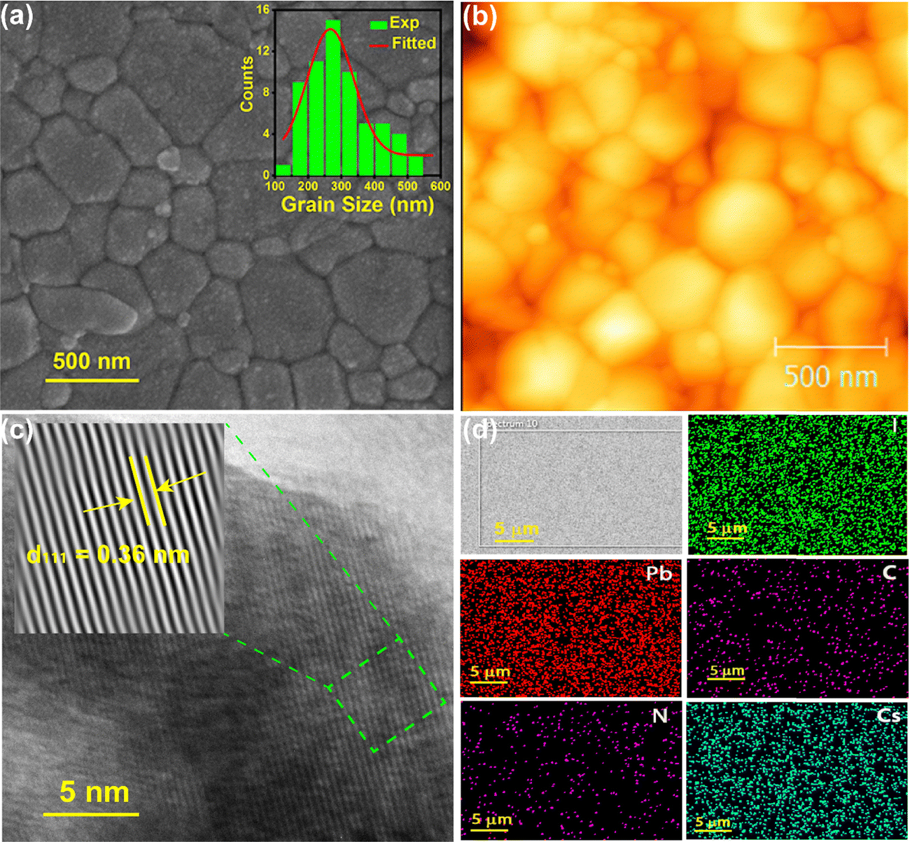
Fig. 2a and b illustrates the morphology of the PVK film, revealing a continuous, pinhole-free film with complete surface coverage. The high-magnification SEM image (Fig. 2a) highlights well-crystallized PVK with densely packed grains ranging from 100 to 600 nm in size. These large grains reduce charge carrier recombination by minimizing grain boundaries, thereby enhancing the photocurrent. The inset provides a grain size distribution diagram, showing an average size of approximately 280 nm. The cross-sectional SEM image (Fig. S4, ESI†) indicates that the average thickness of the FACs film is about 510 nm. AFM was employed to further examine the surface morphology, as shown in Fig. 2b. The local topography data reveal a root-mean-square roughness of 19 nm, indicating that the films are extremely smooth and well suited for efficient charge transport and enhanced photovoltaic performance. The high-resolution TEM (HRTEM) image (Fig. 2c) clearly depicts a well-resolved lattice fringe having an interplanar spacing of 0.36 nm, corresponding to the (111) plane of α-FAPbI3. To verify the crystallinity of the perovskite film prepared for TEM analysis, XRD measurements were performed on the film spin-coated onto a TEM grid. Fig. S5 (ESI†) shows the XRD pattern of the perovskite film deposited on the TEM grid. The characteristic diffraction peaks at 14.18°, 28.37°, 31.78°, and 40.64° correspond to the crystalline planes of the perovskite film, and are consistent with the peaks observed in the XRD pattern of the film deposited on the quartz substrate. The two additional peaks at 43.6° and 50.7° correspond to the Cu signals from the TEM grid. The overall peak intensities of the TEM grid sample are lower than those of the quartz sample due to the smaller film area. The consistent diffraction pattern confirms that the film retains its crystalline quality during TEM sample preparation. Additionally, energy dispersive X-ray spectroscopy (EDS) elemental mapping images (Fig. 2d) confirm the homogeneous distribution of carbon (C), nitrogen (N), cesium (Cs), lead (Pb), and iodine (I) within the film. The EDS spectra and elemental atomic ratios for PVK films are provided in Fig. S6 (ESI†). The atomic percentages of the primary elements in the FACs film closely match the expected stoichiometric composition of FA0.88Cs0.12PbI3.
 |
| | Fig. 2 (a) FESEM image showing large grains in the film; the inset displays the size distribution with the average grain size of 300 nm. (b) AFM image of the perovskite film showing large grains. (c) HRTEM lattice image of the perovskite film; the inset shows the inverse fast Fourier transform (IFFT) lattice image. (d) FESEM image and the corresponding elemental mapping of I, Pb, C, N, and Cs in the film. | |
3.3. Optical characterization
The PVK layer serves as a key material in PVK PDs, with its optical properties playing a crucial role in determining the device performance. We examined the optical properties of the synthesized pure α-FAPbI3 thin film before device fabrication. The PVK film exhibits a broad absorption spectrum that ranges from the ultraviolet to the near-infrared region (350–800 nm).38,42,43Fig. 3a presents the absorption spectra of samples P1, P2, and P3. Among these, sample P2 exhibits the strongest absorption, suggesting enhanced light-harvesting efficiency. The absorbance per unit thickness (A/d) graph is shown in Fig. S7 (ESI†) to provide a clear insight into the higher intrinsic absorption efficiency of the films. While it is generally expected that a thicker perovskite film should result in stronger absorption, several factors can contribute to deviations from this trend. The higher A/d value essentially suggests a higher absorption coefficient of the P2 sample, which implies that P2 has more effective photon utilization, possibly due to its higher crystallinity and minimized scattering or recombination losses. Perovskite film quality significantly influences absorption characteristics. Thicker films (such as P3 with 640 nm thickness) may exhibit increased defect density, suboptimal crystallinity, or light scattering effects, which can reduce effective absorption. For direct bandgap semiconductors, the optical bandgap (Eg) can be extracted from the absorption spectrum using the expression44here, α represents the absorption coefficient, hν is the incident photon energy, and A is a constant. A standard approach to estimate the bandgap is through the Tauc plot, which involves plotting of (αhν)2 against photon energy (hν). By extrapolating the linear segment of the plot, the optical bandgap was determined to be 1.54 eV. To optimize the film thickness for photodetection, steady-state photoluminescence (PL) spectra were recorded for samples P1, P2, and P3 (Fig. 3b). Sample P2 exhibited the lowest PL intensity, which is desirable for photodetection as it suggests efficient charge extraction and reduced recombination losses. This observation is further supported by UV-visible absorption spectra, where the 510 nm-thick film displayed the highest absorption (Fig. 3a), implying an increased generation of photocarriers. The combination of lower PL intensity and higher absorption suggests an optimal balance between light harvesting and charge transport which makes sample P2 the most suitable candidate for photodetection purpose and subsequent device fabrication. To gain deeper insights into the carrier relaxation dynamics in the PVK film, the PL spectrum was deconvoluted. Fig. 3c presents three distinct emission peaks fitted in the PL spectrum at 797 nm, 765 nm, and 830 nm. The primary peak at 797 nm corresponds to band-to-band recombination, representing the intrinsic excitonic emission of the PVK. The lower-intensity peak at 765 nm is attributed to excitonic recombination. The weakest peak at 830 nm is associated with defect-assisted recombination, originating from trap states within the bandgap, likely due to halide vacancies or lattice.45–47 To further validate the above, time-resolved photoluminescence (TRPL) analysis was performed to extract the lifetime of the photoexcited carriers in the film. Fig. 3d presents the TRPL spectra decay profile of the synthesized Pe film. The TRPL data were fitted using a triexponential decay function described as11,38| |  | (3) |
where τ1 is the fast decay component associated with nonradiative recombination from defects, τ2 corresponds to radiative recombination of free carriers in the bulk PVK material, and τ3 is associated with slow carrier recombination processes, such as trap-assisted recombination or charge transfer to an adjacent transport layer, with A1, A2 and A3 representing their relative amplitudes. The average lifetime (τavg) of the carriers was calculated using the relation| |  | (4) |
 |
| | Fig. 3 (a) Absorption spectra of samples P1, P2, and P3. The inset shows the Tauc plot for sample P2. (b) Steady-state PL spectra of samples P1, P2, and P3. (c) Deconvoluted PL spectrum of sample P2 with peak fitting. (d) TRPL decay profile of sample P2 fitted with a tri-exponential decay function. | |
The average lifetime of the carriers in PVK thin film is found to be 9.61 ns.11,41 Detailed parameters for the decay constants and amplitudes are provided in Table S1 (ESI†). The presence of multiple decay components confirms the existence of both radiative and non-radiative recombination pathways. Notably, the weak emission at 830 nm suggests trap-state-mediated recombination, characterized by a shorter lifetime component in TRPL, indicating non-radiative losses. However, the relatively low intensity of these defect-related peaks suggests that trap states have a minimal contribution to the overall emission, which is beneficial for photodetection applications. These findings confirm that the FACs PVK film with low defect density was successfully synthesized via the one-step anti-solvent spin-coating method and exhibits excellent structural and optical properties.
3.4. Characterization of 2D Ti3C2Tx MXene
The phase and crystallinity of the synthesized MX nanosheets were investigated using XRD. The diffraction peaks centered at 2θ = 6°, 17°, 29.1°, and 34.1° correspond to the (002), (004), (006) and (101) planes of MX, confirming the successful exfoliation from the MAX phase (Fig. S8a, ESI†).28,48 The absence of a diffraction peak at 2θ = 39° indicates the successful removal of Al atomic layers and the transition from Ti3AlC2 to Ti3C2Tx.49,50 Raman spectroscopy was also performed to further confirm the phase of Ti3C2Tx. The obtained Raman bands primarily correspond to A1g (out-of-plane vibrational mode of Ti–C) and Eg (in-plane vibrational mode of Ti, C, and surface groups), which match well with previous reports, as shown in Fig. S8b (ESI†).51 The Raman bands at 202.1 cm−1 and 722.7 cm−1 correspond to the A1g mode, while the broader spectral regions ranging from 230 to 470 cm−1 and 532 to 700 cm−1 are associated with the Eg mode.49,51 The XPS spectra of Ti3C2Tx were recorded to analyze the elemental composition and electronic states. The XPS survey spectrum (Fig. S9a, ESI†) clearly shows the presence of C, Ti, O, and F, with no detectable Al signal. This confirms that the Al layer was completely etched away from the MAX phase during the synthesis. The high-resolution Ti 2p spectrum (Fig. S9b, ESI†) of Ti3C2Tx MX was further deconvoluted into four doublet peaks at binding energies of (454.6 and 460.1 eV), (455.3 and 461.2 eV), (456.8 and 462.8 eV), and (459.1 and 464.9 eV). These peaks are attributed to Ti–C, Ti2+, Ti3+, and Ti4+, respectively. The high-resolution O 1s XPS spectrum (Fig. S9c, ESI†) of Ti3C2Tx was deconvoluted into three peaks corresponding to Ti–O (529.4 eV), C–Ti–Ox (531.8 eV), and C–Ti–OHx (533.5 eV). The C 1s spectrum was fitted with peak positions at 281.71 eV and 284.6 eV, corresponding to Ti–C and C–C, respectively (Fig. S9d, ESI†).49 Thus, the XRD, Raman, and XPS analyses confirm the successful synthesis of Ti3C2Tx nanosheets. The morphology of the synthesized Ti3C2Tx MX nanosheets was analyzed using TEM and AFM. The TEM image (Fig. S10a, ESI†) reveals nanosheet-like structures with a well-defined lateral dimension. The lateral size of the nanosheets ranges from 0.11 μm to 0.76 μm. The high-resolution TEM image (Fig. S10b, ESI†) further displays an interplanar spacing of 0.26 nm, corresponding to the (101) plane.48 AFM image (Fig. S10c, ESI†) analysis was conducted to quantify the thickness of the synthesized MX nanosheets. The AFM image and the corresponding height profile (Fig. S10d, ESI†) confirm that the nanosheets are ultrathin, with an average measured thickness of 1.66 nm, indicating the formation of monolayer and bilayer nanosheets.48,49,52
3.5. Photodetector performance
To evaluate the photoelectric conversion efficiency of the device, we first examined its spectral response using symmetric Ag–Ag electrodes under monochromatic light excitation with wavelengths of 405 nm, 450 nm, 532 nm, 650 nm, and 808 nm. Initially, to achieve optimal device performance, the thickness of the PVK film was systematically varied, and its photoresponse was evaluated at 420 nm, 510 nm, and 640 nm. The highest photocurrent was observed for the 510 nm thick film (Fig. S11a, ESI†) at a wavelength of 405 nm, which is consistent with the absorption spectrum. Based on this observation, the device was fabricated using the optimized PVK film thickness. The highest photocurrent was observed at 405 nm for the Ag–PVK–Ag PD, as shown in Fig. S11b (ESI†). This indicates strong light absorption and efficient photogeneration of carriers at 405 nm. Therefore, a 405 nm laser source was used for a detailed investigation of the other device performance characteristics. The device showed no response to the 980 nm laser or to any wavelength beyond it. This result is expected as the absorption edge is at 815 nm (Fig. 3a). This means that the PVK can absorb light and generate charge carriers only for a wavelength of 808 nm or shorter. For the Ag–PVK–Ag PD, I–V characteristics were recorded under dark and illumination (405 nm) at various light intensities ranging from 0.034 to 21.13 mW cm−2 (Fig. S11c, ESI†). The device demonstrated a remarkably low dark current (∼10−10 A at 5 V bias). The photocurrent increased significantly with the increase in light intensity due to the higher charge carrier density under high light intensity. The photocurrent reached ∼10−7 A at an intensity of 21.13 mW cm−2, which is approximately three orders of magnitude higher than the dark current. The I–V curves for the symmetric electrode device show linear behaviour passing through the origin, under both dark and illuminated conditions (Fig. S10d, ESI†). This confirmed the absence of a photovoltaic effect in the symmetric device. These results serve as a baseline for analyzing the effect of asymmetric electrodes on device performance. The I–V characteristics of the MX–PVK–Ag PD were evaluated over a voltage range of −5 V to 5 V. The device exhibited a low dark current in comparison to the Ag–PVK–Ag device. Furthermore, I–V curves of the MX–PVK–Ag PD under 405 nm light illumination with different intensities are presented in Fig. 4a to investigate the device photosensitivity. The deviation of the dark current from zero at 0 V bias is attributed to the presence of built-in electric field/potential and residual charge carriers at the electrode–perovskite interface. In our device, the asymmetric electrode configuration leads to a built-in electric field, which can induce a small leakage current even at zero bias. This behavior indicates that the device operates in a self-biased mode, which is beneficial for low-power operation of the photodetector. More electron–hole pairs are generated with stronger illumination, which results in higher photocurrent in the device.43 The I–V curves under light illumination displayed a slight deviation from the coordinate origin, signifying the emergence of a photovoltage effect. In the Ag–PVK–Ag PD, photo-generated electrons and holes are separated under an applied bias, and both charge carriers are efficiently collected by the Ag electrodes. However, when asymmetric electrodes like MX and Ag are used, a Schottky barrier forms at the PVK–electrode interface due to the difference in their work functions. This mismatch creates a built-in electric field directed from the Ag electrode to the MX electrode that enables the self-powered operation of the device. Upon illumination, charge carriers generated in the PVK diffuse towards the Schottky barrier region at both the interfaces (MX–PVK and Ag–PVK). The unidirectional built-in electric field helps separate these carriers, with holes being extracted by the MX electrode and electrons by the Ag electrode, as explained later in Section 3.7. This leads to photocurrent generation even without an external bias, demonstrating the self-powered nature of the MX–PVK–Ag PD. This is a key feature of the Schottky barrier at the MX–PVK interface, which sets it apart from the ohmic-like behavior observed in the symmetric Ag–PVK–Ag PD. Under the illumination of 21.13 mW cm−2, the device achieved an open circuit voltage (VOC) of 0.6 V and a short-circuit current (ISC) of 37 nA, as shown in Fig. 4b. At 0 V bias, the current increased significantly from 3.54 × 10⁻¹² A to 3.71 × 10⁻⁸ A, yielding a high on–off ratio of 1.05 × 10³. This demonstrates that the MX–PVK–Ag PD can operate effectively without any external power supply. This is the key reason for selecting an asymmetric electrode pair, as it induces a built-in electric field that efficiently separates photogenerated carriers without any external bias. Additionally, the photocurrent under illumination at a 5 V bias for the MX–PVK–Ag PD was notably higher than that of the Ag–PVK–Ag PD. These findings confirm that the asymmetric MX–Ag configuration facilitates self-powered operation while simultaneously improving the optoelectronic performance.53
 |
| | Fig. 4 (a) Current–voltage (I–V) characteristics of the MX–PVK–Ag PD in the dark and under 405 nm illumination at different intensities. (b) I–V characteristics of the device under dark and illumination, with the inset showing the enlarged view at 21.13 mW cm−2. (c) Intensity-dependent photocurrent response of the device at 5 V bias under pulsed 405 nm illumination. (d) Photocurrent as a function of voltage under the illumination of 405 nm light (21.13 mW cm−2). (e) Variation of parameters R, D, and EQE of the MX–PVK–Ag PD with light intensity at 5 V bias and (f) photocurrent growth and decay profiles of the device. | |
Furthermore, the time-resolved photoresponse (I–t) of the MX–PVK–Ag PD was measured under a 405 nm laser at a 5 V bias with varying light intensities, as shown in Fig. 4c. The device exhibited an excellent on–off ratio of 3.5751 × 10⁴ under 21.13 mW cm−2, indicating outstanding switching performance with stable and repeatable operation. The enhancement in photocurrent is due to the built-in potential of the asymmetric device, which minimizes charge recombination and improves carrier separation. We analyzed the variation of photocurrent with different laser power densities by fitting the experimental data to the power law equation,
where
Iph is the photocurrent,
P is the incident light power density,
A is a constant, and
θ is an exponent. For the Ag–PVK–Ag PD, the value of
θ was approximately 0.54, indicating a sublinear relationship between photocurrent and light intensity (Fig. S12, ESI
†). Ideally,
θ should be 1, which signifies that the photocurrent scales proportionally with the light intensity. The observed deviation from the ideal value of
θ suggests non-ideal behavior, likely arising from the recombination loss of photogenerated carriers and trapping of electrons or holes at defects and interface trap sites. In contrast, the asymmetric MX–PVK–Ag PD exhibited an improved power-law fit with
θ ≈ 0.74, indicating a stronger correlation between photocurrent and light intensity. This higher
θ value suggests that the built-in potential introduced by the asymmetric electrode configuration enhances charge separation efficiency. By reducing carrier recombination and minimizing the effects of traps, the device achieves an elevated photocurrent and improved performance under varying illumination intensities. The
I–
t curves of the MX–PVK–Ag PD were measured at different applied voltages.
Fig. 5a shows that the photocurrent increases significantly with higher voltages due to the faster movement of photo-generated charge carriers at higher bias voltages.
 |
| | Fig. 5 Self-biased performance characteristics of the MX–PVK–Ag PD. (a) I–t curves under light illumination (405 nm light) with various intensities. (b) R, D, and EQE as a function of light intensity. (c) Transient photo response of the device. (d) Long-term photo response curves of the device with 405 nm light (21.13 mW cm−2). (e) Temporal response of the photocurrent (I–t) of the device after storing it for several days. | |
To quantitatively assess the performance of the asymmetric MX–PVK–Ag PD, key performance parameters such as responsivity (R), specific detectivity (D*), and external quantum efficiency (EQE) were calculated. R is a crucial parameter that defines the efficiency of a photodetector in converting incident light into an electrical signal. It is given by54,55
| |  | (6) |
where
Iph is the photocurrent (the difference between light current
Il and dark current
Id),
Pin is the incident light intensity, and
A is the effective device area. The symmetric Ag–PVK–Ag PD exhibits a maximum responsivity of 0.62 A W
−1 at a low light intensity of 0.165 mW cm
−2. In contrast, the asymmetric MX–PVK–Ag PD demonstrates an enhanced responsivity with a peak value of 2.58 A W
−1, attributed to its higher photocurrent. However, with an increase in light intensity, recombination effects lead to a reduction in photocurrent, which results in a decrease in responsivity. The variation of
R with light intensity is depicted in
Fig. 4e. Specific detectivity (
D*) quantifies the ability of a photodetector to detect weak light signals. It is expressed as
54,55| |  | (7) |
where
R is the responsivity,
Jd is the dark current density, and
e is the elementary charge.
D* is directly proportional to responsivity and inversely proportional to dark current density. Therefore, minimizing dark current is essential for detecting low-intensity light. In the MX–PVK–Ag PD, the dark current is significantly lower than that of the Ag–PVK–Ag PD, leading to a substantial improvement in
D*. The peak value of
D* for the MX–PVK–Ag PD reaches 1.013 × 10
13 Jones, which is significantly higher than the value (7.80 × 10
11 Jones) observed for the Ag–PVK–Ag PD. External quantum efficiency (EQE) is defined as the ratio of electron–hole pairs collected per unit time to the number of incident photons. It is expressed by
54,55| |  | (8) |
where
e is the elementary charge,
h is Planck's constant,
ν is the frequency of the incident photon,
c is the speed of light, and
λ is the wavelength. EQE can be enhanced by increasing the optical absorption of the active layer and reducing carrier recombination or trapping before collection. Under 405 nm laser illumination at an intensity of 0.165 mW cm
−2, the EQE values for the Ag–PVK–Ag and MX–PVK–Ag photodetectors are 171% and 792%, respectively. These results indicate that the device with asymmetric contacts exhibits much superior performance compared to its symmetric counterpart. This enhancement is attributed to the larger photocurrent generation, resulting from more efficient charge transfer and carrier separation at the Schottky junction. Variation of these parameters with light intensity is shown in
Fig. 4e. The response speed (rise time and fall time) is a key factor in evaluating the photoresponse characteristics of a photodetector. The rise time (
tr) is defined as the duration required for the photocurrent to increase from 10% to 90% of its maximum value, while the fall time (
tf) represents the time taken for the photocurrent to decrease from 90% to 10% of its maximum value.
54 To determine these values, a single cycle photo response data are plotted in an enlarged scale, as shown in
Fig. 4f. For the MX–PVK–Ag PD, the measured rise time and fall time are 110 ms and 75 ms, respectively. In comparison, the Ag–PVK–Ag PD exhibited a slower response with a rise time of 251 ms and a fall time of 105 ms (Fig. S13, ESI
†). The improved performance of the MX–PVK–Ag PD can be attributed to asymmetric electrode-induced charge transport, which enhances carrier extraction and minimizes charge recombination. The asymmetric electrode configuration in the MX–PVK–Ag PD likely generates a unidirectional built-in electric field or preferential charge transport pathways that accelerate the separation and collection of photogenerated carriers. This improves the overall photoresponse speed. Note that the measured photoresponse times are limited by the instrument response time in the photocurrent measurement in the low current range. Hence, the actual device response speed may be much faster than the values shown above.
The self-powered operation of the MX–PVK–Ag PD was investigated in detail under 405 nm laser illumination. The photoresponse was measured without an external bias under periodically modulated light pulses with varying intensities. Fig. 5a presents the I–V characteristics of the PD at different excitation intensities. At an incident intensity of 21.13 mW cm−2, the photocurrent exhibits an enhancement of approximately three orders of magnitude (1.03 × 10³) compared to the dark current, confirming efficient charge carrier generation and separation in the absence of an external bias. Fig. 5b presents the variation of key performance parameters R, D*, and EQE with laser intensity under self-powered operation. The peak values of these parameters are found to be 160 mA W−1, 2.63 × 10¹² Jones, and 49%, respectively. The optimal device performance is observed at an incident power density of 0.042 mW cm−2, beyond which a decrease in performance is noted, likely due to saturation effects or increased recombination losses at higher intensities. The rise time (τr) and fall time (τf) of the PD are measured to be 132 ms and 90 ms, respectively, as shown in Fig. 5c. In addition to high sensitivity, the long-term stability of self-powered PDs under ambient conditions is crucial for their practical application in optoelectronics. Long-term operational stability was confirmed by recording the I–t curves over a continuous illumination period of 3000 seconds at 0 V bias (Fig. 5d). The negligible deviation between the initial and final five cycles demonstrates the operational stability and reliability during prolonged operation. We conducted a storage stability test over a period of ten days in an Ar gas atmosphere inside a glove box. The device retained its photoresponse throughout this period, with only a negligible decrease in photocurrent at 0 V bias compared to the initial measurement on the first day, as shown in Fig. 5e. This demonstrates its excellent stability under these conditions. A comprehensive comparison of key performance parameters for the discussed devices with other literature reports is presented in Table 1. The data clearly demonstrate that our PVK photodetector exhibits superior performance compared to other reported MX-based PVK devices.
Table 1 Comparison of the performance parameters of PVK photodetectors found in the literature with that of the present work
| Device structure |
Operating voltage (V) |
R (A/W) |
D (Jones) |
EQE (%) |
τ
r/τf (ms/ms) |
Ref. |
| MXene/Cs3Bi2I9/MXene |
5 |
6.45 |
9.45 × 10¹¹ |
— |
0.27/2.32 |
56
|
| Pt/(PEA)2PbI4/Ag |
0 |
0.114 |
4.56 × 10¹² |
26.74 |
0.001/0.582 |
53
|
| Al/CH3NH3PbI3/Au |
0 |
0.000232 |
— |
36.16 |
0.071/0.112 |
57
|
| Au/CsPbBr3/Pt |
0 |
0.028 |
1.7 × 10¹¹ |
6 |
230/60 |
58
|
| Au/CsPbBr3/SmB6 |
0 |
0.184 |
3.38 × 10¹⁰ |
44.5 |
100/80 |
59
|
| Au/CH3NH3PbI3 MWs/Ag |
0 |
0.161 |
1.3 × 10¹² |
38.46 |
0.013/0.016 |
60
|
| MX/FA0.88Cs0.12PbI3/Ag |
5 |
2.58 |
1.01 × 10¹³ |
792 |
110/75 |
This work |
| 0 |
0.16 |
2.63 × 10¹² |
49 |
132/90 |
With the rapid progress of optoelectronics, flexible photodetectors have become essential for next-generation wearable and stretchable technologies. The simple solution-based preparation method and the flexible nature of the prepared PVK thin film and MX electrode are suitable for the fabrication of PDs on flexible polyethylene terephthalate (PET) substrates. A flexible PD was fabricated on a PET substrate following the same procedure described in the Experimental section. The mechanical flexibility of the PD was characterized by recording the time-dependent photoresponse under 405 nm light illumination (21.13 mW cm−2) at various bending angles and before and after bending for various times. Fig. 6a illustrates the I–t characteristics at different bending angles of 0°, 60°, 90°, and 120°. The different bending angles were achieved by adjusting the distance between the ends of a holding platform. The largest reduction in photocurrent, approximately 7%, was observed at a 120° bending state. To further assess mechanical stability, the device was subjected to multiple bending cycles at 120° (Fig. 6b). This result shows the exceptional flexibility and mechanical durability of the device, which holds promise for wearable, flexible electronics. The observed reduction in photocurrent under bending conditions is likely due to mechanical strain introducing defects. Such strain can lead to the formation of defects or grain boundary misalignments in the material, which act as traps for charge carriers. These defects may limit charge mobility and slow carrier transport, ultimately reducing the photocurrent. Optimizing material properties to enhance flexibility and mechanical stability is therefore critical for reducing these effects and improving device performance.
 |
| | Fig. 6 Photodetection performance of the flexible perovskite PD. (a) I–t curves of the PD under various bending angles. The insets show the corresponding digital images of the flexible devices. (b) Photocurrent of the PD after multiple bending cycles. | |
3.6. DFT analysis
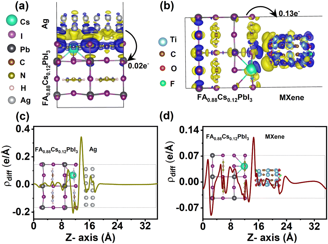
To elucidate the impact of asymmetric electrodes and their role in superior charge separation for enhanced photodetection performance, DFT calculations were performed. Initially, the charge transfers at the FA0.88Cs0.12PbI3/Ag interface were examined, as depicted in Fig. 7(a) and (c). Charge density difference (CDD) calculations were performed to probe charge separation and migration at the interface,22 with yellow regions indicating charge accumulation and blue regions indicating charge depletion. The CDD results (Fig. 7a) reveal electron transfer from Ag to FA0.88Cs0.12PbI3, which confirms the formation of a Schottky junction at the interface arising from the work function difference between the PVK and Ag electrodes. Bader charge analysis quantifies this electron transfer as ∼0.02|e| per unit cell. The plane average charge density difference plot (Fig. 7c) displays pronounced peaks in the FA0.88Cs0.12PbI3 region relative to Ag, further supporting the evidence of electron transfer from Ag to FA0.88Cs0.12PbI3. A similar analysis was conducted for the MX electrode. The CDD plot for the FA0.88Cs0.12PbI3/MX interface (Fig. 7b) demonstrated charge transfer from FA0.88Cs0.12PbI3 to MX, again confirming the formation of a Schottky junction. This observation is further supported by the plane average charge density plot (Fig. 8d), where intense peaks in the MX region define the direction of electron transfer. Bader charge analysis for the FA0.88Cs0.12PbI3/MX interface reveals a charge transfer of approximately 0.13|e|. It is important to note that the direction of electron transfer in the MX electrode was opposite to that observed in the Ag electrode, which confirms the formation of an asymmetric junction at the electrode interfaces. The significantly higher charge transfer in the MX system highlights its superior ability to facilitate the effective separation and transport of photogenerated charge carriers.
 |
| | Fig. 7 DFT charge density difference analysis of perovskite/contact interfaces. Charge density difference (CDD) plot of (a) perovskite and Ag and (b) perovskite and MXene composite from DFT calculations. The charge accumulation and depletion are shown by yellow and blue color patterns in the two regions. The plane average charge density difference plot for (c) perovskite and Ag and (d) perovskite and MXene interface showing two spikes corresponding to charge depletion and charge accumulation. | |
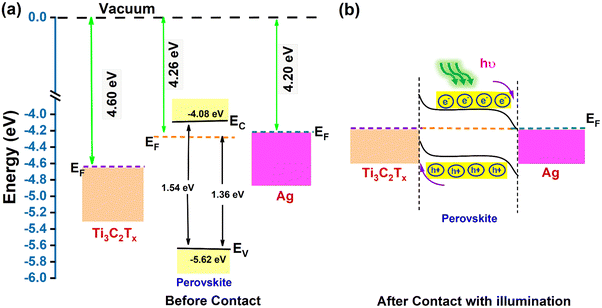 |
| | Fig. 8 (a) Energy band alignment derived from the UPS spectra and (b) band bending across the MXene/perovskite/Ag junction, illustrating the possible charge transfer mechanism in the device under light illumination. | |
3.7. Mechanism of improved photodetection performance
The self-powered photodetection mechanism of the device can be understood by analyzing the band alignment and charge transfer processes at the interfaces between the PVK thin film and the metal electrodes. The difference in work functions between the PVK layer and the metal electrodes causes charge transfer upon contact. This leads to the formation of a Schottky barrier at the PVK–metal interface. In the case of symmetric Ag–Ag electrodes, the photogenerated charge carriers do not have a preferential direction to move within the device. This is because the Schottky barrier formed at the two PVK–Ag contacts is mirror-symmetric. Consequently, the photocurrents generated near each metal electrode are opposite in direction, resulting in a net zero photocurrent. Therefore, an external bias needs to be applied to separate photogenerated carriers and generate photocurrent. In contrast, when an MX electrode is introduced, a Schottky junction forms at the MX–PVK interface. The I–V response of the MX–Ag asymmetric contact configuration demonstrates rectifying behavior, confirming the formation of a directional electric field at the junction. The formation of the Schottky barrier at the MX–PVK–Ag interface can be attributed to the difference in work functions. The formation of the Schottky junction was further verified through DFT simulations (Fig. 7), which showed the formation of a junction at the interfaces of PVK and Ag and PVK and MX. The built-in potential creates a unidirectional stronger local electric field that promotes more effective charge separation, transport, and extraction. To determine the band alignment of the fabricated PD, we examined the energy-level structures of the PVK film and MX electrode using ultraviolet photoelectron spectroscopy (UPS).61–63 The work function (φ) can be calculated using the formula43| | | φ = hv − Ecutoff | (9) |
where hv represents the source energy (He I, 21.2 eV) and Ecutoff is determined by where the secondary electron cut-off intersects at a high binding energy. For the PVK thin film, the measured value of secondary electron cut-off energy is 16.94 eV (Fig S14b, ESI†), and the work function is calculated to be 4.26 eV.41,43 Similarly, the cut-off energy for the MX electrode is 16.6 eV (Fig. S14c, ESI†). So, the Fermi level of MX is found to be at 4.6 eV.48 To determine the separation between the Fermi level and the valence band maxima, we extrapolate the linear part of the spectrum to the energy axis at the low binding energy edge. For the PVK thin film, the value EF − EV is 1.38 eV (Fig. S14a, ESI†). Hence, the valence band maximum (VBM) is estimated to be at −5.62 eV.11,41 The band gap value of the PVK thin film is calculated as 1.54 eV from the UV-visible absorption spectrum (Fig. 3b). So, the conduction band minimum (CBM) is estimated to be at −4.08 eV. For the Ag electrode, the work function is found to be 4.20 eV.64 With these parameters, we constructed a schematic band diagram for the PVK thin film with asymmetric electrodes (MX and Ag) before and after contact, as shown in Fig. 8b. Before contact, the Fermi level (EF) of PVK is close to the conduction band, which indicates that it is an n-type semiconductor. The Fermi level of the MX electrode is below that of the PVK thin film, suggesting a Schottky junction at their interface. After contact, electrons spontaneously flow from PVK to MX due to the higher EF of the PVK layer. This flow continues until equilibrium is reached, and a positively charged layer is formed on the PVK surface and negatively charged electrons are accumulated on the MX surface. This interaction forms a depletion region and causes upward band bending near the junction, resulting in a built-in electric field directed from the PVK to the MX electrode and a Schottky barrier at the interface. Similarly, at the Ag–PVK interface, the difference in work functions establishes another electric field, directed from the Ag electrode to the PVK film, causing the energy bands to bend downward. The combined effect of these built-in electric fields results in a unidirectional electric field across the device. As the built-in electric fields of both metal electrodes (MX and Ag) align in the same direction, they superimpose on the active layer, thereby amplifying the overall built-in electric field. This enhanced electric field efficiently separates and transports the photogenerated carriers, leading to the generation of a photocurrent even at zero bias. Moreover, the Schottky barrier at the MX–PVK junction helps minimize the dark current by limiting the free movement of charge carriers across the junction. The simultaneous presence of two distinct junctions – one at the PVK/Ag interface and the other at the PVK/MX interface – further reduces the dark current while enhancing photocarrier separation under illumination. The barrier potentials formed at the junctions significantly restrict the flow of carriers, resulting in a substantial reduction in dark current when compared to symmetric devices. This unique band alignment and charge transfer mechanism provide the foundation for the self-powered operation of the photodetector, ensuring low dark current and high sensitivity.
4. Conclusion
In summary, we successfully developed a high-performance, self-biased FA-based PVK photodetector by employing asymmetric electrode contacts using MXene and Ag. This strategic design led to the increased and unidirectional built-in electric field at the Schottky junction that facilitates efficient charge separation and collection without external bias. Under self-powered operation, the device exhibited remarkable photodetection capabilities, achieving a responsivity of 160 mA W−1, detectivity of 2.63 × 10¹² Jones, and an external quantum efficiency of 49%. On the other hand, under the external bias, the device exhibited a photoresponsivity of 2.58 A W−1 and a detectivity of 1.013 × 10¹³ Jones, which are significant for practical applications. The ability to achieve such high R, D, and EQE without external power highlights the potential of this design for energy-efficient photodetectors, making it highly suitable for portable and low-power applications. To further explore the real-world applicability of our device, we fabricated a flexible photodetector and evaluated its performance under mechanical deformation. The device retained stable photocurrent responses even after multiple bending cycles. A comprehensive investigation of the charge transfer mechanism was conducted using band alignment data obtained from ultraviolet photoelectron spectroscopy. The band alignment revealed the critical role of the Schottky junction in facilitating efficient charge transport across the MXene/PVK/Ag heterostructure. Additionally, density functional theory calculations were performed to gain a deeper understanding of charge redistribution and interfacial interactions, which further validated our experimental observations. The combination of experimental and theoretical findings presented in this study provides a deeper understanding of how asymmetric electrode engineering on a PVK layer can be utilized to enhance the efficiency and self-powered operation of PVK photodetectors. In essence, our work demonstrates a promising pathway toward high-performance, self-powered, and flexible photodetectors with broad applications in energy-efficient photonics, environmental sensing, and next-generation wearable devices.
Author contributions
DS designed and performed all the experiments, SSR assisted DS, KG performed the simulation, and PKG supervised the project and helped with the design of the study, interpretation of the results, and writing the manuscript.
Data availability
The data supporting this article have been included as part of the ESI.†
Conflicts of interest
The authors declare no competing financial interest.
Acknowledgements
The authors acknowledge the Centre for Nanotechnology and the Central Instruments Facility, IIT Guwahati, for providing access to FETEM, FESEM, XRD, AFM, TRPL, and XPS facilities. We acknowledge the financial support from SERB (Grant number CRG/2021/006397) and MEITY (Grant No. 5(9)/2022-NANO (VOL-II)) for carrying out this work.
References
- X. Hu, X. Li, G. Li, T. Ji, F. Ai, J. Wu, E. Ha and J. Hu, Adv. Funct. Mater., 2021, 31(24), 2011284 CAS.
- W. Tian, Y. Wang, L. Chen and L. Li, Small, 2017, 13(45), 1701848 Search PubMed.
-
H. Qiao, Z. Huang, X. Ren, S. Liu, Y. Zhang, X. Qi and H. Zhang, Adv. Opt. Mater., 2020, 8, 1, 1900765 Search PubMed.
- A. K. Mia, M. Meyyappan and P. K. Giri, Nanoscale, 2024, 16, 8583–8596 CAS.
- M. Ahmadi, T. Wu and B. Hu, Adv. Mater., 2017, 29(41), 1605242 Search PubMed.
- X. Qi, C. Song, W. Zhang, Y. Shi, Y. Gao, H. Liu, R. Chen, L. Shang, H. Tan, F. Tan and H. L. Wang, Adv. Funct. Mater., 2023, 33(19), 2214714 CAS.
- J. Huang, S. He, W. Zhang, A. Saparbaev, Y. Wang, Y. Gao, L. Shang, G. Dong, L. Nurumbetova, G. Yue and Y. Tu, Sol. RRL, 2022, 6(4), 2100839 CAS.
- X. Feng, Y. Gao, X. Huang, J. Wang, C. Dong, G. Yue, F. Tan and S. De Wolf, Small, 2024, 20(44), 2403267 CrossRef CAS PubMed.
- F. Cao, L. Bian and L. Li, Energy Mater. Dev., 2024, 2, 9370018 Search PubMed.
- R. Siavash Moakhar, S. Gholipour, S. Masudy-Panah, A. Seza, A. Mehdikhani, N. Riahi-Noori, S. Tafazoli, N. Timasi, Y. F. Lim and M. Saliba, Adv. Sci., 2020, 13(7), 1902448 Search PubMed.
- B. Yu, Z. Xu, H. Liu, Y. Liu, K. Ye, Z. Ke, J. Zhang and H. Yu, ACS Appl. Mater. Interfaces, 2024, 16, 2408–2416 CrossRef CAS PubMed.
-
F. Wang, X. Zou, M. Xu, H. Wang, H. Wang, H. Guo, J. Guo, P. Wang, M. Peng, Z. Wang, Y. Wang, J. Miao, F. Chen, J. Wang, X. Chen, A. Pan, C. Shan, L. Liao and W. Hu, Adv. Sci., 2021, 8, 14, 2100569 Search PubMed.
- C. Bao, J. Yang, S. Bai, W. Xu, Z. Yan, Q. Xu, J. Liu, W. Zhang and F. Gao, Adv. Mater., 2018, 30(38), 1803422 CrossRef PubMed.
- L. Dou, Y. M. Yang, J. You, Z. Hong, W. H. Chang, G. Li and Y. Yang, Nat. Commun., 2014, 5, 5404 CrossRef CAS PubMed.
- H. Zhou, Z. Song, C. R. Grice, C. Chen, J. Zhang, Y. Zhu, R. Liu, H. Wang and Y. Yan, Nano Energy, 2018, 53, 880–886 CrossRef CAS.
- Z. Gao, H. Zhou, K. Dong, C. Wang, J. Wei, Z. Li, J. Li, Y. Liu, J. Zhao and G. Fang, Nanomicro Lett., 2022, 14, 215 CAS.
- S. P. Senanayak, B. Yang, T. H. Thomas, N. Giesbrecht, W. Huang, E. Gann, B. Nair, K. Goedel, S. Guha, X. Moya, C. R. Mcneill, P. Docampo, A. Sadhanala, R. H. Friend and H. Sirringhaus, Understanding charge transport in lead iodide perovskite thin-film field-effect transistors, Sci. Adv., 2017, 3, e1601935 CrossRef PubMed.
- L. Zhang, H. Zhou, Y. Chen, Z. Zheng, L. Huang, C. Wang, K. Dong, Z. Hu, W. Ke and G. Fang, Nat. Commun., 2024, 15, 1609 CrossRef CAS PubMed.
- W. Wu, J. Zhang, C. Liu, J. Zhang, H. Lai, Z. Hu and H. Zhou, Adv. Sci., 2024, 11(46), 2410303 CrossRef CAS PubMed.
-
Z. Wu, S. Liu, Z. Hao and X. Liu, Adv. Sci., 2023, 10, 19, 2207174 Search PubMed.
- X. Chen, Z. Shi, Y. Tian, P. Lin, D. Wu, X. Li, B. Dong, W. Xu and X. Fang, Mater. Horiz., 2021, 8, 2929–2963 RSC.
- S. He, Z. Lan, B. Zhang, Y. Gao, L. Shang, G. Yue, S. Chen, Z. Shen, F. Tan and J. Wu, ACS Appl. Mater. Interfaces, 2022, 14, 43576–43585 CrossRef CAS PubMed.
-
H. Xu, A. Ren, J. Wu and Z. Wang, Adv. Funct. Mater., 2020, 30, 24, 2000907 Search PubMed.
- X. Jiang, A. V. Kuklin, A. Baev, Y. Ge, H. Ågren, H. Zhang and P. N. Prasad, Phys. Rep., 2020, 848, 1–58 CrossRef CAS.
- A. Iqbal, J. Hong, T. Y. Ko and C. M. Koo, Korea Nano Technol. Res. Soc., 2021, 8, 9 CAS.
- K. Montazeri, M. Currie, L. Verger, P. Dianat, M. W. Barsoum and B. Nabet, Adv. Mater., 2019, 31(43), 1903271 CrossRef CAS PubMed.
- W. Deng, H. Huang, H. Jin, W. Li, X. Chu, D. Xiong, W. Yan, F. Chun, M. Xie, C. Luo, L. Jin, C. Liu, H. Zhang, W. Deng and W. Yang, Adv. Opt. Mater., 2019, 7(6), 1801521 CrossRef.
- A. Ren, J. Zou, H. Lai, Y. Huang, L. Yuan, H. Xu, K. Shen, H. Wang, S. Wei, Y. Wang, X. Hao, J. Zhang, D. Zhao, J. Wu and Z. Wang, Mater. Horiz., 2020, 7, 1901–1911 RSC.
- B. Lyu, M. Kim, H. Jing, J. Kang, C. Qian, S. Lee and J. H. Cho, ACS Nano, 2019, 13, 11392–11400 CrossRef CAS PubMed.
-
D. Hao, J. Zou and J. Huang, Infomat, 2020, 2, 1, 139–169 Search PubMed.
-
Y. Wang, D. Li, L. Chao, T. Niu, Y. Chen and W. Huang, Appl. Mater. Today, 2022, 28, 101509 Search PubMed.
- Y. Tian, Y. Li, C. Hu, Y. Yang, D. Chen and G. Shen, ACS Appl. Mater. Interfaces, 2023, 15, 13332–13342 CrossRef CAS PubMed.
- W. Deng, H. Huang, H. Jin, W. Li, X. Chu, D. Xiong, W. Yan, F. Chun, M. Xie, C. Luo, L. Jin, C. Liu, H. Zhang, W. Deng and W. Yang, Adv. Opt. Mater., 2019, 7(6), 1801521 CrossRef.
- J. P. Perdew, K. Burke and M. Ernzerhof, Generalized Gradient Approximation Made Simple, Phys. Rev. Lett., 1996, 77, 3865 CrossRef CAS PubMed.
- H. J. Monkhorst and J. D. Pack, Special points for Brillonin-zone integrations, Phys. Rev. B, 1976, 13, 5188 CrossRef.
- K. Momma and F. Izumi, J. Appl. Crystallogr., 2008, 41, 653–658 CrossRef CAS.
- N. Zhou, Y. Shen, Y. Zhang, Z. Xu, G. Zheng, L. Li, Q. Chen and H. Zhou, Small, 2017, 13(23), 1700484 CrossRef PubMed.
- M. Qu, Y. Tian, Y. B. Cheng, J. Zhong and C. Zhang, Adv. Opt. Mater., 2022, 10(24), 2201741 CrossRef CAS.
- Z. Lu, C. Lou, A. Cheng, J. Zhang and J. Sun, J. Alloys Compd., 2022, 919, 165831 CrossRef CAS.
- J. W. Lee, D. H. Kim, H. S. Kim, S. W. Seo, S. M. Cho and N. G. Park, Adv. Energy Mater., 2015, 5(20), 1501310 CrossRef.
- X. Sun, F. Deng, S. Li, Y. Li, X. Lv, Y. Z. Zheng and X. Tao, Sol. RRL, 2022, 6(9), 2200303 CrossRef CAS.
- F. X. Liang, J. Z. Wang, Z. X. Zhang, Y. Y. Wang, Y. Gao and L. B. Luo, Adv. Opt. Mater., 2017, 5(22), 1700654 CrossRef.
- D. Sahu, S. Debnath, S. Ghosal and P. K. Giri, ACS Appl. Mater. Interfaces, 2024, 16(37), 49544–49555 CAS.
- M. Zhang, F. Zhang, Y. Wang, L. Zhu, Y. Hu, Z. Lou, Y. Hou and F. Teng, Sci. Rep., 2018,(8), 11157 Search PubMed.
- D. Guo, D. Bartesaghi, H. Wei, E. M. Hutter, J. Huang and T. J. Savenije, J. Phys. Chem. Lett., 2017, 8, 4258–4263 CAS.
- A. Dobrovolsky, A. Merdasa, J. Li, K. Hirselandt, E. L. Unger and I. G. Scheblykin, J. Phys. Chem. Lett., 2020, 11, 1714–1720 CAS.
- E. V. Peán, S. Dimitrov, C. S. De Castro and M. L. Davies, Phys. Chem. Chem. Phys., 2020, 22, 28345–28358 RSC.
-
K. Ghosh and P. K. Giri, Carbon, 216, 2024, 118515 Search PubMed.
- S. S. Roy, K. Ghosh, M. Meyyappan and P. K. Giri, ACS Appl. Nano Mater., 2023, 6, 23357–23369 CrossRef CAS.
- S. Sahare, M. Solovan, M. Smirnova, B. Scheibe, M. Jancelewicz, G. Nowaczyk, M. Kempiński and M. Ziółek, J. Mater. Chem. C, 2024, 12, 8357–8367 RSC.
- A. Sarycheva and Y. Gogotsi, Chem. Mater., 2020, 32, 3480–3488 CrossRef CAS.
- A. Lipatov, M. Alhabeb, M. R. Lukatskaya, A. Boson, Y. Gogotsi and A. Sinitskii, Adv. Electron. Mater., 2016, 2(12), 1600255 CrossRef.
- J. Yan, F. Gao, W. Gong, Y. Tian and L. Li, RSC Adv., 2022, 12, 25881–25889 RSC.
- W. H. Gao and C. Chen, Nano Energy, 2024, 128, 109904 CrossRef CAS.
- X. Lu, J. Li, Y. Zhang, Z. Han, Z. He, Y. Zou and X. Xu, Adv. Photonics Res., 2022, 3(5), 2100335 CrossRef.
- Y. Tian, Y. Li, C. Hu, Y. Yang, D. Chen and G. Shen, ACS Appl. Mater. Interfaces, 2023, 15, 13332–13342 CrossRef CAS PubMed.
- M. I. Saidaminov, M. A. Haque, J. Almutlaq, S. Sarmah, X. H. Miao, R. Begum, A. A. Zhumekenov, I. Dursun, N. Cho, B. Murali, O. F. Mohammed, T. Wu and O. M. Bakr, Adv. Opt. Mater., 2016, 5(2), 1600704 CrossRef.
- J. Ding, H. Fang, Z. Lian, J. Li, Q. Lv, L. Wang, J. L. Sun and Q. Yan, CrystEngComm, 2016, 18, 4405–4411 RSC.
- Z. Liu, G. Cao, Z. Guan, Y. Tian, J. Liu, J. Chen, S. Deng and F. Liu, J. Mater. Chem. C, 2024, 12, 17395–17402 RSC.
- C. Y. Wu, W. Peng, T. Fang, B. Wang, C. Xie, L. Wang, W. H. Yang and L. B. Luo, Adv. Electron. Mater., 2019, 5(5), 1900135 Search PubMed.
- X. Gao, Z. Su, S. Qu, W. Zhang, Y. Gao, S. He, Z. Wang, L. Shang, G. Dong, G. Yue, F. Tan and Z. Wang, J. Mater. Chem. C, 2021, 9, 13500–13508 CAS.
- Y. Gao, Z. Xiao, M. Cui, M. I. Saidaminov, F. Tan, L. Shang, W. Li, C. Qin and L. Ding, Adv. Mater., 2024, 36(9), 2306373 CrossRef CAS PubMed.
- S. He, L. Shang, Y. Gao, Y. Shi, F. Tan, X. Chen and G. Yue, J. Alloys Compd., 2022, 896, 162864 CrossRef CAS.
- D. Hao, D. Liu, S. Zhang, L. Li, B. Yang and J. Huang, Adv. Opt. Mater., 2022, 10(5), 2100786 CrossRef CAS.
Footnote |
| † Electronic supplementary information (ESI) available: Schematic of the fabrication process, height profile, XPS survey spectra, cross-sectional FESEM image, XRD spectra, EDS spectra, absorption spectra, XRD and Raman spectra, XPS spectra, TEM and AFM analysis images, photodetector performance, power law analysis, UPS spectra, TRPL data and calculation of R and D. See DOI: https://doi.org/10.1039/d5tc00968e |
|
| This journal is © The Royal Society of Chemistry 2025 |
Click here to see how this site uses Cookies. View our privacy policy here. 
 Open Access Article
 This Open Access Article is licensed under a Creative Commons Attribution-Non Commercial 3.0 Unported Licence
 *ab
*ab