
Plasma-activated copper-alkanolamine precursor paste for printed flexible antenna: formulation, mechanism, and performance evaluation†
Wendong
Yang
 *abc,
Zihao
Guo
a,
Michael
Hengge
c and
Emil J. W.
List-Kratochvil
*bc
*abc,
Zihao
Guo
a,
Michael
Hengge
c and
Emil J. W.
List-Kratochvil
*bc
aSchool of Electronic and Information Engineering, Liaoning Technical University, Huludao City, 125105, China. E-mail: yangwendong@lntu.edu.cn
bInstitut für Physik, Institut für Chemie, Center for the Science of Materials Berlin, Humboldt-Universität zu Berlin, Berlin 12489, Germany. E-mail: emil.list-kratochvil@hu-berlin.de
cHelmholtz-Zentrum Berlin für Materialien und Energie GmbH, Berlin 14109, Germany
First published on 31st October 2024
Abstract
Copper-based pastes have attracted significant attention for printed electronic applications because of their low cost and high conductivity. Copper precursor pastes are easier to prepare, exhibit long-term stability and do not have oxidation issues during preparation and storage, when compared to copper micro-sized flakes and nanoparticle pastes. Up to now, copper precursor pastes activated by plasma have been rarely studied, and their activation mechanism is not clear. Furthermore, little attention has been paid to the application of these pastes in wireless electronic devices. In this paper, therefore, we formulated a plasma-activated copper–alkanolamine complex precursor paste for antenna applications. The paste was formulated only using copper(II) formate and excess 2-amino-2-methyl-1,2-propanediamine, which exhibited favorable flowability for screen printing. Copper films with good conductivity were produced on PET substrates by plasma sintering this paste. The effects of plasma sintering time on the properties of the copper film were explored and correlations between them were established. A possible plasma activation mechanism was proposed. Finally, a flexible ultra-wideband antenna with notch properties was fabricated with the copper paste, demonstrating its feasibility in wireless electronics applications.
1. Introduction
Over the past decade, there has been an increasing interest in employing printed electronic technologies to fabricate electronic devices.1–3 Unlike conventional photolithography and etching techniques that require complicated and lengthy preparation steps, this additive manufacturing technology allows for the efficient creation of low-cost electronic devices4–6 while also making better use of material resources with less waste. Printed electronic technology has been used to fabricate electronic devices such as electronic circuits,7,8 displays,9–12 solar cells,13,14 sensors,15–17 and antennas18–23 on a variety of flexible substrates, providing devices with flexibility, transparency, wearability and other characteristics.24–27Screen printing is one of the popular patterning techniques for printed electronics, favored for its wide substrate applicability and facile fabrication process.28 Low-cost, highly conductive, low-temperature processable and printable pastes are becoming key materials restricting the development of screen-printed flexible electronic devices.29 Up to now, pastes based on materials such as graphene,30–33 carbon nanotubes,34–37 conducting polymers,38–41 silver,42–46 and copper29,47–50 have demonstrated significant potential for screen printing across a wide range of applications.51 Among these materials, silver paste is the most favored one due to its high conductivity and excellent stability,52–57 and it has been used to fabricate a wide range of flexible electronic devices. For instance, Lim et al.44 developed a silver paste by using unsaturated polyester resin as binder polymers and silver particle as conductive material. They fabricated transparent electrode patterns by screen printing the silver paste on flexible polyurethane and polyester films. Shukla et al.43 have developed a AgNW-based paste for screen printing of flexible and stretchable electronics.
Copper pastes have emerged as a cost-effective alternative to silver pastes due to their low price and comparable conductivity. Copper conductive pastes can be divided into three categories: traditional micro-sized flakes and powders type,58 nanoparticle type29,48 and precursor type.59 Among them, copper precursor pastes are simple to prepare and exhibit long-term stability and resistance to oxidation during preparation and storage processes since copper exists in their oxidized form in such pastes. Additionally, these pastes can be converted to copper at lower temperatures, making them suitable for flexible temperature-sensitive substrates. For copper precursor pastes, a post-processing is usually required to give the paste specific electronic properties. However, copper is highly susceptible to oxidation during this process,60 which will decrease the conductivity of copper pastes. Currently, two approaches have been adopted to alleviate oxidation of the copper precursor pastes during post-processing. One is the use of a special post-treatment process, such as photonic sintering, plasma sintering, chemical sintering and thermal sintering using a protective (N2, Ar) or reducing atmosphere (formic acid or H2),61 while the other is to adjust the paste recipe to make it self-reducible. For instance, copper precursor pastes were formulated through the control of the mole ratio between copper(II) acetate and 2-amino-2-methyl-1-propanol for screen printing.62 The printed copper patterns displayed metalized copper with low resistivity (30 μΩ cm) and dense film structure after sintering at 180 °C under an N2 environment for 10 minutes. Copper precursor paste with a high copper loading was developed by mixing excess Cu(OH)2 with formic acid for printed electronics, producing a volume resistivity of 30 μΩ cm for the film at 200 °C under a N2 environment for 3 minutes.63
Plasma sintering provides an efficient way for the rapid and low-temperature metallization of metal conductive pastes, which is typically accomplished by exposing printed metal patterns to low-pressure argon plasma.64–66 Plasma generation produces a variety of excited species as well as UV irradiation, causing the decomposition of the paste and allowing direct contact of metal particles.64 The temperature during plasma sintering is usually less than 100 °C, making this method suitable for the applications on flexible temperature-sensitive substrates.
Up to now, copper precursor pastes activated by plasma have been rarely studied. The majority of existing plasma sintering cases mainly focus on metal silver inks,67–70 copper inks71,72 or silver or copper nano pastes.65,66,73–75 The only few reports on copper precursor pastes were developed for thermal sintering.62,63 Besides, the plasma activation mechanism is not clear. The sintering of copper precursor paste is different from the copper nano paste, which is a type of copper particle synthesis process. The existing research on the decomposition and reduction mechanism of copper precursor and the formation rules of the copper film are based on thermal sintering process, and most of them are just descriptions and inductions of experimental phenomena. Moreover, little attention has been paid to the use of these pastes in wireless electronic devices. The only studies have focused on radio frequency identification (RFID) tag antennas.76 Therefore, it will be interesting to develop plasma-activated copper precursor paste for flexible antenna applications and get insight into its plasma activation mechanism.
In this paper, a plasma-activated copper–alkanolamine complex paste for screen printing was formulated. The paste was formulated only using copper(II) formate and excess 2-amino-2-methyl-1,2-propanediamine (AMP), which exhibited favorable flowability suitable for screen printing. Copper films with good conductivity were produced on PET substrates by plasma sintering this paste. Correlations between sintering time and the properties of the copper films were established. A possible plasma activation mechanism was given. A compact, flexible antenna was fabricated with the copper paste, which exhibited the ultra-wideband and notch characteristics, demonstrating its feasibility in wireless electronics applications.
2. Experimental section
2.1 Synthesis of copper–alkanolamine complex paste
Copper(II) formate tetrahydrate [Cu(HCOO)2·4H2O, Cuf·4H2O], acquired from Alfa Aesar, was selected as the copper source. 2-Amino-2-methyl-1-propanol [(CH3)2C(NH2)CH2OH, AMP], obtained from Adamas, served as the complexing agent. All chemicals were used without additional treatment. Copper–alkanolamine complex paste was synthesized by mixing copper(II) formate tetrahydrate precursor and AMP solvent with a molar ratio of 1![[thin space (1/6-em)]](https://www.rsc.org/images/entities/char_2009.gif) :3 for 30 minutes under vigorous stirring. The resulting copper paste is dark blue and viscous in appearance.
:3 for 30 minutes under vigorous stirring. The resulting copper paste is dark blue and viscous in appearance.
2.2 Fabrication of films, circuits, and antenna
Polyethylene terephthalate (PET) substrates of 15 mm × 15 mm (thickness 0.12 mm) were employed as the substrates. Prior to screen printing, all of the PET substrates were cleaned with deionized water and ethanol. Fabrication of conductive films, circuits and antenna pattern were performed on a screen printer (Shenzhen Delo Technology Development Co., Ltd, China) with a 200-mesh screen. Plasma sintering was employed to process the printed samples. The power was set to 300 W, with a duration spanning 15–35 minutes, and the flow rate of Ar gas below 50 mL min−1.2.3 Characterization and measurement
The surface functional groups and molecular structure of Cuf·4H2O, AMP, and the copper paste were investigated using a Fourier transform infrared (FT-IR) spectrometer (Thermo Scientific Nicolet iS50). The thermal decomposition behaviors of the copper paste were characterized using a simultaneous thermal analyzer (DSC-TG, HITACHI STA200) under a nitrogen atmosphere with a heating rate of 10 °C min−1. The viscosity of the copper paste was measured using a rotary viscometer (NDJ-8S). The crystalline phase of copper films obtained at different sintering times was analyzed by a Rigaku Ultima IV X-ray diffractometer (XRD, Cu Kα radiation, λ = 0.15418 nm). X-ray photoelectron spectroscopy (XPS, Thermo ESCALAB 250Xi) with Al Kα radiation was utilized to analyze the chemical state of copper films. Energy calibration was achieved by setting the C 1s line at 284.80 eV. The field-emission scanning electron microscope (SEM, ZEISS Sigma 300) was utilized to observe the surface and cross-sectional morphology of the copper films. A surface energy-dispersive spectrometer (EDS, Oxford Xplore30) was employed for examining the surface morphology and chemical composition of copper films. The resistivity of copper films was measured by a four-point probe tester (HPS2524). The S11 values of the antenna were measured using a vector network analyzer (Keysight E5063A).3. Results and discussion
3.1 Synthesize of copper precursor paste
Copper precursor pastes are usually made from copper precursors such as organic or inorganic copper salts, and copper oxides with solvents/ligands/reducing agents and additives.61 The selection of copper precursor is critical because it determines the thermal and electrical properties of the final copper paste. For printed electronic applications on flexible temperature-sensitive substrates, one must consider three factors when selecting a proper copper precursor, its decomposition temperature, copper content and solubility in common solvents. Taken together, copper carboxylates are good choices because they are easy to be converted into metal copper at low temperature. Compared to other copper carboxylates, Cuf decomposes at a temperature near 220 °C, yielding metallic copper with high conductivity and without organic residues. Additionally, Cuf releases gases like CO and H2 during the decomposition process that help prevent the oxidation of copper. Therefore, Cuf·4H2O was chosen as the precursor for the paste preparation. To dissolve and disperse sparingly soluble Cuf·4H2O powder, an alkanolamine, 2-amino-2-methyl-1-propanol (AMP) was used as the ligand. This amine has two functional groups with lone electron pairs: an amino group (–NH2) and a hydroxyl group (–OH). These lone pairs can occupy the vacant d orbitals of the Cu2+ ion, forming coordination bonds between alkanolamine and Cuf·4H2O, thereby resulting in a liquid copper–alkanolamine complex (Fig. 1a). Due to the high viscosity and reducing properties of AMP, the resulting deep-blue copper complex does not require the addition of reducing agents and binders when used as a paste (Fig. 1b). By adjusting the mixing ratio of Cuf·4H2O and AMP, a highly conductive copper precursor paste suited for low-temperature sintering and screen-printable was obtained.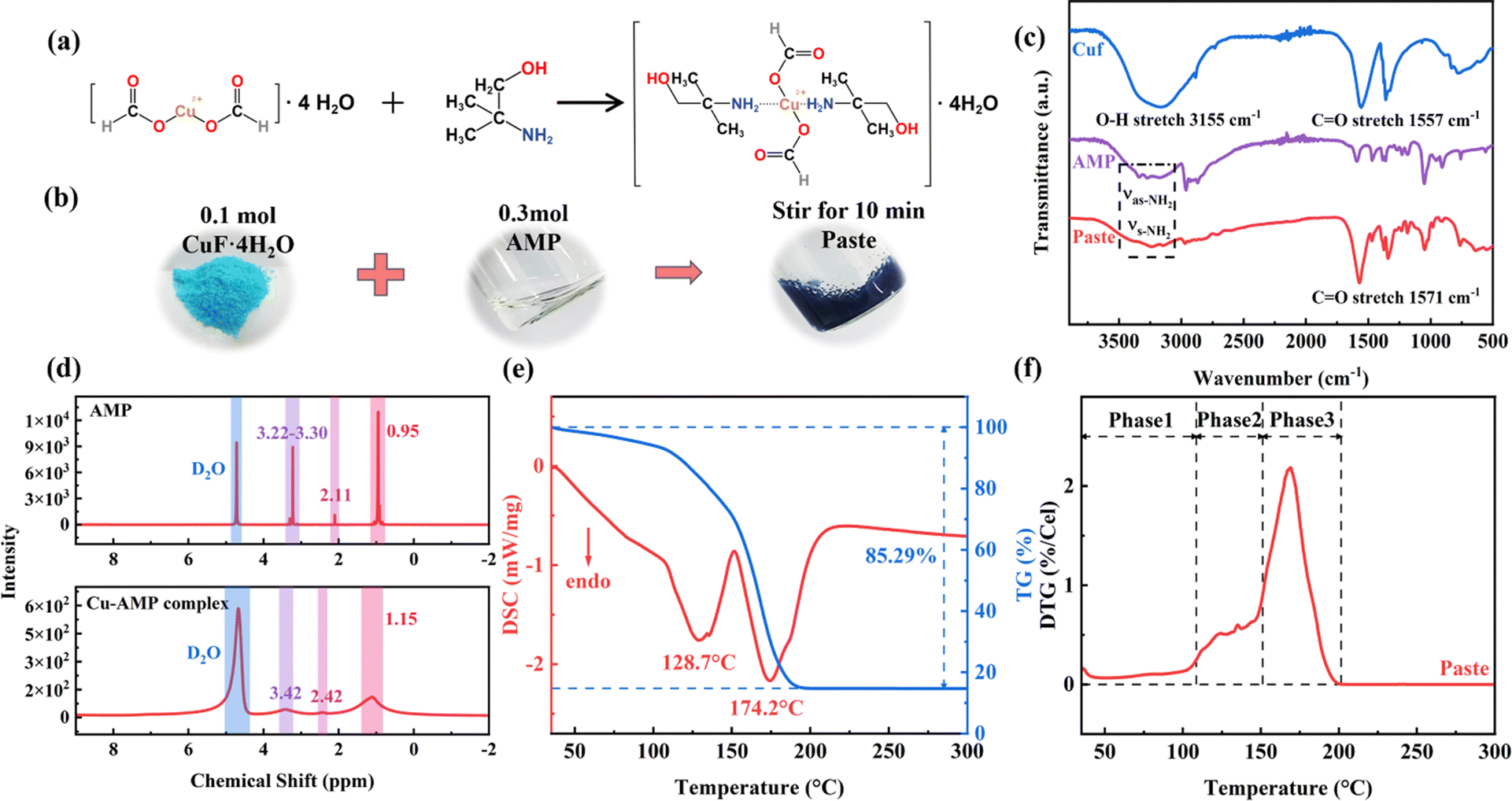 | ||
| Fig. 1 (a) Complexation reaction of Cuf·4H2O and AMP, (b) synthesis process of deep-blue copper precursor paste, (c) FT-IR spectra of Cuf·4H2O, AMP, and the paste, (d) 1H-NMR spectra of AMP and Cuf–AMP complex, D2O solvent for both, (e) DSC-TG and (f) DTG results of the paste. | ||
FT-IR analysis was employed to confirm the above-mentioned coordination process. As illustrated in Fig. 1c, for Cuf·4H2O, the peak at 3155 cm−1 is attributed to the stretching vibration of the hydroxyl group (–OH) of the crystalline water in copper(II) formate tetrahydrate, while the peak at 1557 cm−1 corresponds to the stretching vibration of Cu (II)-bonded carboxyl group in Cuf. For AMP, the asymmetric stretching vibration (νas-NH2) and symmetric stretching vibration (νs-NH2) of the amino group (–NH2) appear at 3340.17 cm−1 and 3266.51 cm−1, respectively. After complex, new coordination bonds are formed, causing the νas-NH2 and νs-NH2 peaks to shift to 3239.16 cm−1 and 3147.74 cm−1, respectively. The interaction between Cu2+ and the carboxyl group breaks, resulting in free carboxyl groups, and the C![[double bond, length as m-dash]](https://www.rsc.org/images/entities/char_e001.gif) O peak shifts to 1571 cm−1. These changes confirm the formation of a Cuf–AMP complex.
O peak shifts to 1571 cm−1. These changes confirm the formation of a Cuf–AMP complex.
The 1H-NMR results of the AMP and the Cuf–AMP complex in Fig. 1d also confirm this reaction process. Due to the coordinating effect of copper ions, the electron density around the amine hydrogen (NH2) decreases, leading to a significant shift in its chemical shift, from 2.11 to 2.42. Meanwhile, the chemical shifts of other hydrogens also change, particularly those adjacent to the amine group like CH3 or –CH2 group, from 0.95 to 1.15 or 3.22–3.30 to 3.42. These changes further verified the formation of the Cuf–AMP complex, which is similar to the complexation processes of Cuf with primary and secondary amines as well as pyridines reported in ref. 77 and 78.
3.2 Characterization of copper precursor paste
3.3 Printability
The printability of the as-prepared copper precursor paste was evaluated using a rotational viscometer, an optical microscope and a drop-shaped analyzer. As illustrated in Fig. 2a–c, the deep-blue copper paste demonstrates favorable flowability, with a measured viscosity of 1805 ± 52 cP. This value falls within the range of 500 to 5000 cP required by the screen-printing, indicating that the paste could be screen-printed. For screen printing, a high viscosity is generally beneficial because it helps maintain the integrity of the printed pattern, ensuring sharp edges and preventing the paste from spreading or bleeding outside the desired area. High viscosity also helps the paste stay on the screen during the printing process, reducing smearing and enabling more precise deposition of material. | ||
| Fig. 2 Photographs of (a) the synthesized copper precursor paste and (b) its screen-printing process, (c) wettability, (d) and (e) optical images of lines with different widths printed on PET substrates, (f) adhesion test of the screen-printed copper film and (g) application of conductive circuit. | ||
The wettability of the paste was also investigated here. A contact angle of 77 ± 1.3° was determined on the glass substrate. For printing fine features on hydrophobic substrates, a large contact angle can indeed be beneficial for achieving high-resolution patterns. A larger contact angle indicates that the printed material has less wettability on the substrate, which helps prevent the spreading of the paste. This reduced spread enables more precise and well-defined edges, allowing for finer feature resolution.
During the screen-printing process, the copper paste passes smoothly through the screen to produce the designed patterns without clogging or dripping, demonstrating good printability. A high-quality copper paste should also exhibit continuity and uniformity after printing. Here, lines with lengths of 5 cm and widths of 5 mm, 4 mm, 3 mm, 2 mm, 1 mm, 0.5 mm, 0.4 mm and 0.3 mm were printed and plasma-sintered (300 W, 30 minutes) on the PET substrate to examine the printing quality of the paste, as shown in Fig. 2d and e. The copper paste exhibits good resolution and fineness. At the same time, optical microscopic graphic details reveal that the printed lines have good edge definition and surface smoothness, with no visible breaks or burrs.
Adhesion is an important property for ensuring the stability and durability of printed circuits and patterns. A tape test procedure was used to assess the adhesion strength of the plasma-sintered copper paste on the PET substrate, as illustrated in Fig. 2f. The majority of the copper film remained on the PET substrate when the tape was peeled off. By the ASTM adhesion test standard, the copper paste earned a 3B adhesion rating. This value can be enhanced by using a small amount of polyvinylpyrrolidone (PVP, 1%) in the paste. To evaluate the applicability of the copper paste in printed flexible electronics, a bulb was connected with the printed conductive lines. After applying a voltage of 3 V, the bulb was lighted successfully (Fig. 2g), even when the conductive lines were bent.
The above results revealed that the prepared copper paste has good screen-printability, and can produced copper patterns with relatively high resolution, accuracy and favorable adhesion on flexible PET substrate. These characteristics make the paste promising for use in printed flexible electronic and communication devices.
3.4 Properties of plasma-sintered copper films
Plasma sintering provides benefits over thermal and chemical sintering in terms of sintering time and the impurities of the products. Plasma's high energy density allows materials to be rapidly sintered and densified at lower temperatures. This is highly useful for applying copper paste on flexible temperature-sensitive surfaces. Furthermore, the oxidation problem with copper particles or films produced can be avoided. Therefore, plasma sintering was chosen for the sintering of the screen-printed copper paste.XRD analysis was used to determine the physical phase and crystal structure of the films sintered for different time, as shown in Fig. 3a. A clear relationship between sintering time and the formation of copper crystals is displayed.
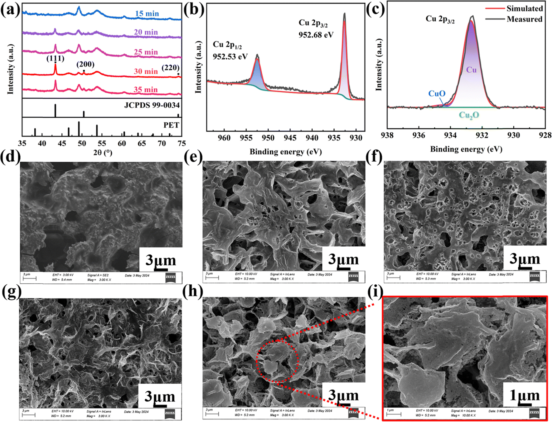 | ||
| Fig. 3 (a) XRD results of the copper films plasma-sintered for different time, (b) and (c) XPS results of the copper film plasma-sintered for 30 minutes, and SEM results of the copper films plasma-sintered for (d) 15, (e) 20, (f) 25, (g) 30, and (h) and (i) 35 minutes. | ||
When the sintering time is shorter than 15 minutes, only the diffraction peaks of the PET substrate are visible, indicating that the copper–alkanolamine complex has not been decomposed or reduced to metal copper. In other words, the energy provided by the shorter sintering duration is not enough to break down the complex or initiate crystallization of copper.
As the sintering time increases to 20–30 minutes, distinctive diffraction peaks emerge at 2θ values of 43.316°, 50.448°, and 74.124°. These peaks correspond to the (111), (200), and (220) planes of the face-centered cubic (FCC) structure of copper, as indexed by the Joint Committee on Powder Diffraction Standards (JCPDS) 99-0034. This demonstrates that the copper–alkanolamine complex has been transformed to copper crystals.
However, when the sintering time exceeds a certain threshold, such as 35 minutes, the benefits of increased time plateau. Prolonged sintering may result in excessive grain growth, potentially causing defects such as grain boundary coarsening or unwanted oxidation at the surface, which could degrade the film's overall structural integrity. Consequently, the XRD peaks show a slight reduction in intensity due to these effects, indicating that an optimal sintering time is crucial for achieving the best crystallinity and minimizing defects. In our case, it is 30 minutes.
Considering the limits of XRD in detecting amorphous oxides, XPS analysis was performed on the film sintered with plasma for 30 minutes to confirm whether copper oxides are present. As shown in Fig. 3b, the Cu 2p1/2 and Cu 2p3/2 peaks of the film exhibits satellite peaks, indicating the presence of copper in different valence states. Further peak fitting on the spectrum of Cu 2p3/2 was performed to separate the contribution of metallic copper (Cu0), cuprous (Cu+), and cupric (Cu2+) states, with fitted peaks at 932.711 eV, 933.262 eV and 934.533 eV, respectively (Fig. 3c). The film's composition was eventually determined to be 97.29% metallic copper (Cu0), 0.01% cuprous oxide (Cu2O), and 2.70% cupric oxide (CuO), indicating that it is mainly composed of copper. This also demonstrates the advantage of plasma in copper paste sintering. The presence of small amounts of copper oxides may be attributed to human error during sample handling. Specifically, if the sample is removed from the plasma chamber before it reaches an appropriate cooling temperature, minimal oxidation of the surface can occur.
SEM analysis was conducted to investigate the microstructure of copper films sintered for different times. As shown in Fig. 3d, after 15 minutes of sintering, the film was composed of a large number of colloidal substances. Combined with the paste recipe and XRD results, it can be inferred that these substances were undecomposed copper–alkanolamine complexes. As the sintering time increases from 20 to 30 minutes (Fig. 3e–g), the colloidal substance became less and the remaining colloidal particles (the copper–alkanolamine complexes) gradually aggregated to form a three-dimensional network film structure in which copper particles were produced. Further increasing the sintering time to 35 min resulted in a flake-belt integrated morphology (Fig. 3h and i), which was composed of two distinct segments: belts with a shot diameter and irregular flakes consisting of spherical copper particles. The junction of these two different segments located at the edge. This is quite different from the microstructure of the copper film derived from thermal-sintered copper–alkanolamine complexes.47,59,79 Compared to single spherical or flaky particles, this flake-belt integrated morphology is helpful in improving electrical properties at low temperatures.
Semi-quantitative EDS analysis was also conducted on samples sintered for 20, 25, 30, and 35 minutes. Three elements, Cu, O and C, were detected. The mass percentage of Cu in the film sintered for 30 minutes reach up to 95.13% (Fig. 4a and b), which is consistent with the XPS results. Samples sintered for 20 and 25 minutes have relatively high O and C contents, indicating the presence of incompletely decomposed copper–alkanolamine complexes, which verifies the previous analyses. When the sintering time is increased to 35 minutes, the mass percentage of Cu decreases, while the mass percentage of O increases, perhaps from the oxidation of copper film. These results demonstrate that plasma sintering time has a significant impact on the purity and composition of copper film. Shorter sintering time fails to completely decompose the copper–alkanolamine complex, whereas longer times cause the film to densify less. A sintering time of 30 minutes is ideal, as it ensures the adequate decomposition of the copper–alkanolamine complex while also facilitating the copper film formation with three-dimensional network structure.
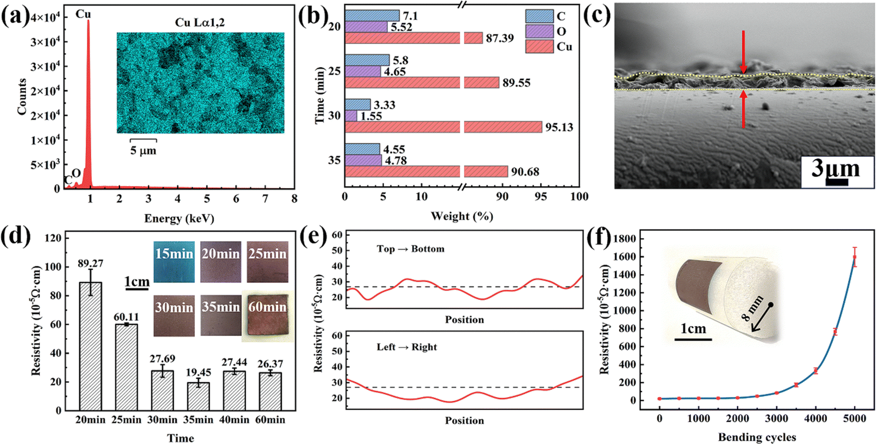 | ||
| Fig. 4 (a) and (b) EDS mapping results, (c) cross-section of the copper film plasma-sintered for 30 minutes, (d) resistivity against the sintering time of the copper films, (e) surface electrical properties across different locations of the copper films and (f) bendability of the copper film plasma-sintered for 30 minutes. | ||
The resistivities of copper films at different sintering times were also explored. The average thickness of the copper films was about 1.54 ± 0.5 μm (Fig. 4c). The resistivity of the films sintered for different times were calculated using the measured sheet resistance and thickness. When the sintering time was less than 15 minutes, the film was not totally dry and showed blue color in appearance (inset of Fig. 4d) with no or very few copper particles produced (not detected by XRD in Fig. 3a). Therefore, it exhibited a high resistivity that exceeded the measurement range of the four-probe instrument. As the sintering time increased, the copper–alkanolamine complex decomposed and copper nanocrystals were produced to create a conductive net structure, thereby resulting a decrease in resistivity (19.45 × 10⁻⁵ Ω cm).
The improvement in conductivity with the time can be easily understood. For copper precursor paste, its electrical performance of copper precursor pastes is principally determined by three factors: particle size, the degree of organic residues, and film density. As the treatment duration increases, the plasma can provide sufficient thermal energy to enable adequate decomposition of the Cuf–AMP complexes and AMP, as well as promote the growth, better connection and aggregation of generated copper particles, thereby resulting in an increased conductivity. However, further increasing the plasma treatment time will not lead to a significant improvement in the electrical properties of the film since a conductive path has been formed. Instead, a prolonged treatment time will damage the PET substrate. In our experiments, after 60 minutes of sintering, the PET substrate of the copper film has deformed and turned yellow in appearance. Therefore, after consideration, 30 minutes was finally determined to be the optimal sintering time, which can ensure the required electrical properties without damaging the PET substrate.
Additionally, to analyze the uniformity of the printed copper patterns, surface electrical properties across different locations of the copper films sintered for 30 minutes were measured (Fig. 4e). The resistivity of the film at the center is lower than that at the edges, indicating that the copper film's uniformity is not consistent across its surface. This variation suggests that the sintering process may have been more effective in the center, which is associated with the shrinkage effect of AMP during the sintering process.
Here, we also assessed the bendability of the printed copper film. The tests were performed by compressing the film at a given radius of curvature (r = 8 mm). As seen in Fig. 4f, the film's resistivity increases slightly after 3000 bending cycles, suggesting an acceptable flexibility for various applications. When bending cycles approach 5000, the film's resistivity increases to 15 times its initial value, possibly due to decreased contact between copper nanoparticles in the film.
In summary, the above analyses show that sintering time has an important influence on the decomposition of copper–alkanolamine complex and the formation of copper grains. After 30 minutes of plasma sintering, a copper film with good electrical properties and three-dimensional network structure was obtained.
3.5 Plasma activation mechanism
Plasma sintering is a promising technique for rapid densification of advanced new materials with various applications. However, limited data are available on the sintering mechanism of copper complex pastes. A popular view is that during the plasma sintering process, a higher pulse current is applied to the electrode, and microscopic discharges in the gaps between powder particles generate plasma, thereby causing sintering.80,81Here, MS analysis was employed to gain a better understanding of the plasma-sintering mechanism of the as-prepared copper precursor paste. In combination with the microstructure of the sintered films in Fig. 3d–i, a possible sintering mechanism was proposed.
The sintering of copper precursor paste is considered as a type of solventless particle synthesis process. In the initial stage, an electric field in the gaps between copper–alkanolamine complex was created and high-temperature plasmas were excited under the action of a pulse current so that it caused a discharge between adjacent complex particles, leading to a local heating on the surface of these complexes. When the sinter time is shorter than 15 minutes, the heat creates a temperature insufficient to cause decomposition of the Cuf–AMP complex and access AMP but could cause the shrinkage and aggregation of complexes, thus resulting in a partly dry blue film with a high resistivity (Fig. 5a and 4d).
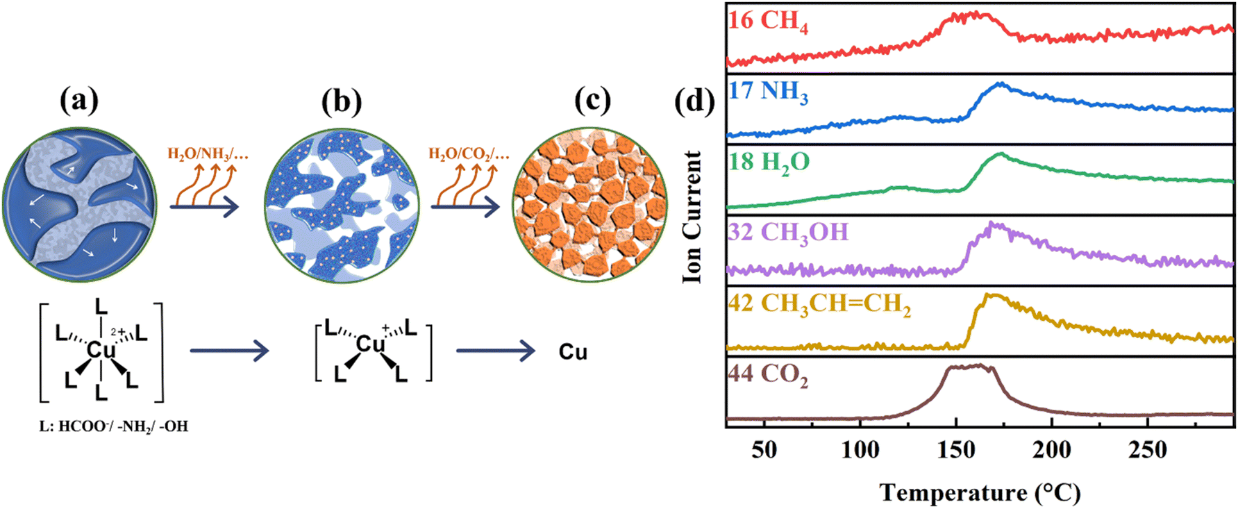 | ||
| Fig. 5 Plasma activation mechanism of the copper precursor paste: (a–c) Copper paste state in early, mid, and late sintering stages, and (d) corresponding MS results. | ||
When the sintering time is longer than 20 minutes, evaporation and decomposition of AMP and the Cuf–AMP complex occurred due to the heat accumulation. The vapor recoiling force push the paste into isolated islands, eventually forming clusters of various sizes with the final loss of the liquids. Since the temperature generated by local heating reaches the decomposition temperature of the copper complex at this time (Fig. 5b), copper particles were produced in these islands and forms a three-dimensional network as proved by Fig. 3a, e–g.
As the sintering time increases to 35 minutes, undecomposed Cuf–AMP complexes are sputtered onto the surfaces of adjacent copper particles produced at high speed under the action of an electric field, and are decomposed to produce copper particles to form connections. At this time, due to the local temperature caused by the discharge effect is higher than the decomposition end temperature of the copper complex, thereby leading to a film with a robust three-dimensional network structure and lower resistivity (Fig. 5c, 3h and i).
In combination with the MS results during the heating in Fig. 5d, it can be inferred that the following chemical reactions occur during the plasma sintering process. Reactions (1) took place in 15 minutes (below 120 °C), while reactions (2) and (3) occurred after 20 minutes (above 175 °C).
 | (1) |
 | (2) |
 | (3) |
4. Antenna applications
A compact, flexible UWB copper antenna with notch properties was proposed on a PET substrate to prove the possibilities of the prepared copper complex paste in wireless electronics applications. The antenna was designed to operate at frequencies ranging from 2.9 to 14 GHz, with two notch characteristics that suppress the signals in the Indian National Satellite (INSAT) band (4.5–4.8 GHz) and the International Telecommunication Union (ITU) band (8.025–8.4 GHz). It consists of a radiating patch, a microstrip line, and a grounding plate, with a total dimension of 22 × 15 × 0.12 mm3. The radiating patch is composed of a circle and a rectangle. A 50 Ω microstrip line is employed to feed the antenna. Fig. 6 depicts the structure of the designed antenna, and the values for each parameter are presented in Table 1. More information on the antenna structure design and structural parameter optimization procedure can be seen in ESI.† | ||
| Fig. 6 Schematic view of the designed antenna. | ||
| Parameter | Value | Parameter | Value | Parameter | Value |
|---|---|---|---|---|---|
| W | 15 | W1 | 10 | W2 | 6 |
| W3 | 0.64 | W4 | 0.43 | W5 | 6 |
| W6 | 1.4 | W7 | 6.4 | L | 22 |
| L1 | 6.8 | L2 | 7.1 | L3 | 4.75 |
| L4 | 2.2 | L5 | 6.6 | L6 | 7.11 |
| L7 | 6 | L8 | 0.65 | R1 | 6.1 |
| R2 | 2.5 |
The antenna prototype was fabricated on a PET substrate by screen printing of the as-prepared copper complex paste (Fig. 7a), and its actual performance was tested on a vector network analyzer (Fig. 7b). The printed antenna exhibits a brick-red color and a compact structure. The measured S11 values and radiation pattern (Fig. 7c and d) show that the antenna operates in a range of 2.9 to 14.0 GHz, covering the desired UWB frequency band with one desired notch property. Failure to achieve the second notch may be associated with the properties of copper complex paste and printing quality. The antenna pattern has a conductivity one order of magnitude lower than an ideal copper conductor, a porous surface structure caused by the gas releases during the decomposition process, and a printed size that deviates slightly from the designed one. Overall, the antenna fabricated achieves the ultra-wideband performance and has certain notch characteristics, demonstrating the feasibility of the copper complex paste in wireless electronics applications.
 | ||
| Fig. 7 (a) Fabrication processes of antenna prototype, (b) photo of the antenna prototype under the measurement, and (c) and (d) the measured S11 values and radiation patterns at 3.5 GHz. | ||
In addition to wireless electronic applications, this antenna design can be utilized in various fields, including Internet of Things (IoT) devices, medical telemetry, smart textiles, and automotive applications. Its flexibility allows for seamless integration into wearable technology, enhancing communication and data transmission in dynamic environments. For instance, Geyikoglu et al. reported a UWB flexible antenna with dual notch bands for wearable biomedical devices.82 The proposed antenna is printed on a 12.5 μm thick Kapton substrate, featuring circular radiating elements and square-shaped slits in the ground plane to achieve dual notch bands. Its efficient performance, simple fabrication, flexibility, and thin profile make it suitable for integration into flexible and wearable biomedical devices. We are currently exploring wearable applications for these antennas, as their compact design makes them ideal for smart clothing and health monitoring devices. This integration could improve the functionality of wearables by ensuring reliable wireless communication while maintaining comfort and convenience. For this paper, our research primarily focuses on the development of cost-effective materials suitable for antenna fabrication.
We believe that expanding the applications of copper-based conductive paste will enhance the performance and affordability of antennas, making them more accessible for various wearable technologies and improving their integration into smart clothing and health monitoring devices.
5. Conclusions
A copper precursor conductive paste has been developed for the fabrication of printed flexible circuits and wireless electronic devices. The paste was formulated by a facile process using copper(II) formate as a precursor and AMP as ligand, which can decompose to copper by low temperature plasma sintering. It displays good fluidity on PET substrates, allowing for pattern formation via screen printing. The influences of sintering time on the physical phase, composition, microstructure and electrical properties of the copper film from the prepared copper paste were investigated, and correlations between them were established. A possible plasma activation mechanism was proposed: the high-temperature spark plasma was generated in the gaps between complexes at the beginning of sintering, fast, efficient sintering is then achieved under the combined action of Joule heating and electrical diffusion in the sintering process. A flexible UWB antenna with notch properties was finally fabricated on a flexible PET substrate by screen-printing of the as-prepared copper precursor paste, demonstrating its feasibility in wireless electronics applications.Author contributions
Dr Wendong Yang conceived the idea and wrote the draft of the manuscript. Mr Zihao Guo carried out the preparation and characterization of the copper paste, as well as the design, fabrication and performance assessment of the antenna. All authors analyzed the data, discussed the results and commented on the manuscript.Data availability
All relevant data are within the manuscript and its Additional files.Conflicts of interest
All authors declare that they have no conflict of interest.Acknowledgements
The authors express their gratitude for the funds from the Department of Science & Technology of Liaoning Province (No. 2022-BS-329), CSC scholarship (No. 202308210202) and Liaoning Technical University (Grant No. 21-1039). The authors thank Hangzhou Yanqu Information Technology Co. Ltd for their assistance in the characterization of the copper paste and films. This work was completed in the Liaoning Key Laboratory of Radio Frequency and Big Data for Intelligent Applications and the framework of the Joint Lab GEN_FAB.References
- L. Wang, F. Xia, W. Xu, G. Wang, S. Hong, F. Cheng, B. Wu and N. J. A. F. M. Zheng, Adv. Funct. Mater., 2023, 33, 2215127 CrossRef CAS.
- Y. Khan, A. Thielens, S. Muin, J. Ting, C. Baumbauer and A. C. Arias, Adv. Mater., 2020, 32, 1905279 CrossRef CAS.
- K. Liu, B. Ouyang, X. Guo, Y. Guo and Y. Liu, npj Flexible Electron., 2022, 6, 1 CrossRef CAS.
- S. Bi, B. Gao, X. Han, Z. He, J. Metts, C. Jiang and K. Asare-Yeboah, Sci. China: Technol. Sci., 2023, 1–24 Search PubMed.
- Y. Li, M. Misra and S. Gregori, IEEE Trans. Compon., Packag., Manuf. Technol., 2018, 8, 1307–1315 CAS.
- H. Abdolmaleki, P. Kidmose and S. Agarwala, Adv. Mater., 2021, 33, 2006792 CrossRef CAS.
- Y. Wang, H. Guo, J.-j Chen, E. Sowade, Y. Wang, K. Liang, K. Marcus, R. R. Baumann and Z.-s Feng, ACS Appl. Mater. Interfaces, 2016, 8, 26112–26118 CrossRef CAS.
- A. Komolafe, R. Torah, Y. Wei, H. Nunes-Matos, M. Li, D. Hardy, T. Dias, M. Tudor and S. Beeby, Adv. Mater. Technol., 2019, 4, 1900176 CrossRef CAS.
- X. Ji, W. Liu, Y. Yin, C. Wang and F. Torrisi, J. Mater. Chem. C, 2020, 8, 15788–15794 RSC.
- R. Rai, D. Mantione, T. A. Gazis, A. J. Cartlidge and P. D. Matthews, J. Mater. Chem. C, 2023, 100, 11325–11332 Search PubMed.
- Y. Liang, C. Liu, M. Zhao, R. Wang, D. Zhang, C. Wang, L. Zhou, L. Wang, Z. Xie and J. Peng, ACS Appl. Mater. Interfaces, 2020, 12, 20714–20721 CrossRef CAS.
- Y. Jiang, Q. Ma and S. Dong, Appl. Mater. Today, 2024, 37, 102119 CrossRef.
- D. H. Shin, J. H. Kim, J. H. Kim, C. W. Jang, S. W. Seo, H. S. Lee, S. Kim and S.-H. Choi, J. Alloys Compd., 2017, 715, 291–296 CrossRef CAS.
- M. Rawat, E. Jayaraman, S. Balasubramanian and S. S. K. Iyer, Adv. Mater. Technol., 2019, 4, 1900184 CrossRef CAS.
- X. Yang, J. Gui, C. Dong, J. Zhao and R. Xu, ACS Appl. Nano Mater., 2023, 6, 21679–21687 CrossRef CAS.
- Z. Wu, X. Yang and J. Wu, ACS Appl. Mater. Interfaces, 2021, 13, 2128–2144 CrossRef CAS PubMed.
- C. Mackin, V. Schroeder, A. Zurutuza, C. Su, J. Kong, T. M. Swager and T. s Palacios, ACS Appl. Mater. Interfaces, 2018, 10, 16169–16176 CrossRef CAS.
- X. Fan, X. Zhang, Y. Li, H. He, Q. Wang, L. Lan, W. Song, T. Qiu and W. Lu, Nanoscale Horiz., 2023, 8, 309–319 RSC.
- I. Ibanez-Labiano, M. S. Ergoktas, C. Kocabas, A. Toomey, A. Alomainy and E. Ozden-Yenigun, Appl. Mater. Today, 2020, 20, 100727 CrossRef.
- Z. Li, S. K. Sinha, G. M. Treich, Y. Wang, Q. Yang, A. A. Deshmukh, G. A. Sotzing and Y. Cao, J. Mater. Chem. C, 2020, 8, 5662–5667 RSC.
- E. Sowade, F. Göthel, R. Zichner and R. R. Baumann, Appl. Surf. Sci., 2015, 332, 500–506 CrossRef CAS.
- W. Yang, H. Sun, Z. Guo and X. Zhao, ACS Appl. Nano Mater., 2023, 6, 9628–9638 CrossRef CAS.
- J. Zhu, Z. Hu, S. Zhang, X. Zhang, H. Zhou, C. Xing, H. Guo, D. Qiu, H. Yang and C. Song, ACS Appl. Mater. Interfaces, 2022, 14, 12855–12862 CrossRef CAS.
- Y. Zhang, Y. Tan, J. Lao, H. Gao and J. Yu, ACS Nano, 2023, 17, 9681–9693 CrossRef CAS PubMed.
- S. Huang, Y. Liu, Y. Zhao, Z. Ren and C. F. Guo, Adv. Funct. Mater., 2019, 29, 1805924 CrossRef.
- Y. Zhang, L. Zhang, K. Cui, S. Ge, X. Cheng, M. Yan, J. Yu and H. Liu, Adv. Mater., 2018, 30, 1801588 CrossRef.
- Z. Wu, Y. Wang, X. Liu, C. Lv, Y. Li, D. Wei and Z. Liu, Adv. Mater., 2019, 31, 1800716 CrossRef.
- K. Arapov, E. Rubingh, R. Abbel, J. Laven, G. de With and H. Friedrich, Adv. Funct. Mater., 2016, 26, 586–593 CrossRef CAS.
- S. Hong, C. Liu, S. Hao, W. Fu, J. Peng, B. Wu and N. Zheng, npj Flexible Electron., 2022, 6, 17 CrossRef CAS.
- Q. Lin, F. Zhang, X. Xu, H. Yang, Q. Mao, D. Xian, K. Yao and Q. Meng, Nanomaterials, 2023, 13, 2630 CrossRef CAS.
- L. Liu, Z. Shen, X. Zhang and H. Ma, J. Colloid Interface Sci., 2021, 582, 12–21 CrossRef CAS PubMed.
- J. Zhu, W. Song, J. Peng, Y. Yin, B. Xu and C. Wang, J. Coat. Technol. Res., 2022, 1–9 Search PubMed.
- F. Zhao, H. Quan, S. Zhang, Y. Xu, Z. Zhou, G. Chen and Q. Li, Polymers, 2023, 15, 356 CrossRef CAS.
- D. Hu, W. Zhu, Y. Peng, S. Shen and Y. Deng, J. Mater. Sci. Technol., 2017, 33, 1113–1119 CrossRef CAS.
- N. A. Vacirca, J. K. McDonough, K. Jost, Y. Gogotsi and T. P. Kurzweg, Appl. Phys. Lett., 2013, 103 Search PubMed.
- V. D. Phadtare, V. G. Parale, G. K. Kulkarni, N. B. Velhal, H.-H. Park and V. R. Puri, Ceram. Int., 2017, 43, 4612–4617 CrossRef CAS.
- X. Tang, K. Wu, X. Qi, H.-j Kwon, R. Wang, Z. Li, H. Ye, J. Hong, H. H. Choi and H. Kong, ACS Appl. Nano Mater., 2022, 5, 4801–4811 CrossRef CAS.
- H. Yuk, B. Lu, S. Lin, K. Qu, J. Xu, J. Luo and X. Zhao, Nat. Commun., 2020, 11, 1604 CrossRef CAS.
- T. Chen, Q. Chen, G. Liu and G. Chen, J. Appl. Polym. Sci., 2018, 135, 45943 CrossRef.
- K.-Y. Shin, M. Kim, J. S. Lee and J. Jang, Sci. Rep., 2015, 5, 13615 CrossRef PubMed.
- J. S. Lee, M. Kim, J. Oh, J. Kim, S. Cho, J. Jun and J. Jang, J. Mater. Chem. A, 2015, 3, 7029–7035 RSC.
- T. Inui, H. Koga, M. Nogi, N. Komoda and K. Suganuma, Adv. Mater., 2014, 27, 1112–1116 CrossRef.
- D. Shukla, Y. Liu and Y. Zhu, Nanoscale, 2023, 15, 2767–2778 RSC.
- C. K. Lim, Y. S. Lee, S. H. Choa, D. Y. Lee, L. S. Park and S. Y. Nam, Int. J. Polym. Sci., 2017, 2017, 9623620 Search PubMed.
- Z. Li, X. Zhang, J. Shan, C. Liu, X. Guo, X. Zhao and H. Yang, Mater. Res. Express, 2022, 9, 066401 CrossRef CAS.
- Y. Chen, X. Wang, B. Zhang, W. Ma and W. Chen, J. Mater. Sci.: Mater. Electron., 2021, 32, 22119–22128 CrossRef CAS.
- Y. Farraj, M. Grouchko and S. Magdassi, Chem. Commun., 2015, 51, 1587–1590 RSC.
- A. Yabuki and N. Arriffin, Thin Solid Films, 2010, 518, 7033–7037 CrossRef CAS.
- W. Li, W. Li, J. Wei, J. Tan and M. Chen, Mater. Chem. Phys., 2014, 146, 82–87 CrossRef CAS.
- K.-Y. Shin, J. S. Lee, J.-Y. Hong and J. Jang, Chem. Commun., 2014, 50, 3093–3096 RSC.
- Q. Huang and Y. Zhu, Adv. Mater. Technol., 2019, 4, 1800546 CrossRef.
- M. Park, J. Im, M. Shin, Y. Min, J. Park, H. Cho, S. Park, M.-B. Shim, S. Jeon and D.-Y. Chung, Nat. Nanotechnol., 2012, 7, 803–809 CrossRef CAS.
- N. Komoda, M. Nogi, K. Suganuma, K. Kohno, Y. Akiyama and K. Otsuka, Nanoscale, 2012, 4, 3148–3153 RSC.
- Y. Liu, J. Hao, X. Zheng, C. Shi and H. Yang, J. Mater. Chem. C, 2023, 11, 5009–5017 RSC.
- H. Hong, J. Hu and X. Yan, ACS Appl. Mater. Interfaces, 2019, 11, 27318–27326 CrossRef CAS.
- L. Song, A. C. Myers, J. J. Adams and Y. Zhu, ACS Appl. Mater. Interfaces, 2014, 6, 4248–4253 CrossRef CAS.
- J. Liang, K. Tong and Q. Pei, Adv. Mater., 2016, 28, 5986–5996 CrossRef CAS PubMed.
- S. Wu, H. Qin and P. Li, J. Univ. Sci. Technol. Beijing, 2006, 13, 250–255 CrossRef CAS.
- D.-H. Shin, S. Woo, H. Yem, M. Cha, S. Cho, M. Kang, S. Jeong, Y. Kim, K. Kang and Y. Piao, ACS Appl. Mater. Interfaces, 2014, 6, 3312–3319 CrossRef CAS.
- S. Wünscher, R. Abbel, J. Perelaer and U. S. Schubert, J. Mater. Chem. C, 2014, 2, 10232–10261 RSC.
- W. Li, Q. Sun, L. Li, J. Jiu, X.-Y. Liu, M. Kanehara, T. Minari and K. Suganuma, Appl. Mater. Today, 2020, 18, 100451 CrossRef.
- H. Naderi-Samani, R. S. Razavi and R. Mozaffarinia, Heliyon, 2022, 8, e12624 CrossRef CAS PubMed.
- S. K. Tam, K. Y. Fung and K. M. Ng, J. Mater. Sci., 2017, 52, 5617–5625 CrossRef CAS.
- C. Cano-Raya, Z. Z. Denchev, S. F. Cruz and J. C. Viana, Appl. Mater. Today, 2019, 15, 416–430 CrossRef.
- W. Yang, X. Zhao, Z. Guo, H. Sun and E. J. List-Kratochvil, Sci. Rep., 2024, 14, 11407 CrossRef CAS.
- Y. Gao, H. Zhang, J. Jiu, S. Nagao, T. Sugahara and K. Suganuma, RSC Adv., 2015, 5, 90202–90208 RSC.
- T. S.-W. Leung, E. Ramon and C. Martínez-Domingo, Adv. Eng. Mater., 2023, 25, 2200834 CrossRef CAS.
- N. Wang, Y. Liu, W. Guo, C. Jin, L. Mei and P. Peng, Nanotechnology, 2020, 31, 305301 CrossRef CAS.
- S. Wünscher, S. Stumpf, J. Perelaer and U. S. Schubert, J. Mater. Chem. C, 2014, 2, 1642–1649 RSC.
- W. Yang, F. Hermerschmidt, F. Mathies and E. J. List-Kratochvil, J. Mater. Sci.: Mater. Electron., 2021, 32, 6312–6322 CrossRef CAS.
- Y.-T. Kwon, Y.-I. Lee, S. Kim, K.-J. Lee and Y.-H. Choa, Appl. Surf. Sci., 2017, 396, 1239–1244 CrossRef CAS.
- C. E. Knapp, E. A. Metcalf, S. Mrig, C. Sanchez-Perez, S. P. Douglas, P. Choquet and N. D. Boscher, ChemistryOpen, 2018, 7, 850–857 CrossRef CAS PubMed.
- X. Lu, Z. Lv, Y. Sun, M. Murugesan, C. Zhou, X. Zhang and J. Liu, J. Electron. Mater., 2022, 51, 6310–6319 CrossRef CAS.
- F. M. Wolf, J. Perelaer, S. Stumpf, D. Bollen, F. Kriebel and U. S. Schubert, J. Mater. Res., 2013, 28, 1254–1261 CrossRef CAS.
- N. Alayli, F. Schoenstein, A. Girard, K.-L. Tan and P.-R. Dahoo, Mater. Chem. Phys., 2014, 148, 125–133 CrossRef CAS.
- A. M. Marindra, P. Pongpaibool, W. Wallada and S. Siwamogsatham, Int. J. Microw. Wirel. Technol., 2017, 9, 469–479 CrossRef.
- Y. Dong, Z. Lin, X. Li, Q. Zhu, J.-G. Li and X. Sun, J. Mater. Chem. C, 2018, 6, 6406–6415 RSC.
- C. Paquet, T. Lacelle, X. Liu, B. Deore, A. J. Kell, S. Lafrenière and P. R. Malenfant, Nanoscale, 2018, 10, 6911–6921 RSC.
- W. Yang, Z. Guo, X. Zhao, X. Zhang and E. J. List-Kratochvil, Langmuir, 2024, 40, 7095–7105 CrossRef CAS.
- S.-X. Song, Z. Wang and G.-P. Shi, Ceram. Int., 2013, 39, 1393–1396 CrossRef CAS.
- Z.-H. Zhang, Z.-F. Liu, J.-F. Lu, X.-B. Shen, F.-C. Wang and Y.-D. Wang, Scr. Mater., 2014, 81, 56–59 CrossRef CAS.
- M. Dilruba Geyikoglu, Analog Integr. Circuits Signal Process., 2023, 1–12 Search PubMed.
Footnote |
| † Electronic supplementary information (ESI) available. See DOI: https://doi.org/10.1039/d4tc03346a |
| This journal is © The Royal Society of Chemistry 2025 |