
 Open Access Article
 This Open Access Article is licensed under a Creative Commons Attribution-Non Commercial 3.0 Unported Licence
Enhancing the efficiency of non-fullerene organic solar cells by using a volatilizable solid additive system†
Walia Binte
Tarique
 *,
Ashraful Hossain
Howlader
,
Shahriyar Safat
Dipta
,
Ayush
Pratik
and
Ashraf
Uddin
*
*,
Ashraful Hossain
Howlader
,
Shahriyar Safat
Dipta
,
Ayush
Pratik
and
Ashraf
Uddin
*
School of Photovoltaic and Renewable Energy Engineering, University of New South Wales, Sydney, NSW 2052, Australia. E-mail: w.binte_tarique@unsw.edu.au; a.uddin@unsw.edu.au
First published on 7th March 2025
Abstract
The morphology of the active layer mostly affects the photovoltaic efficiency of organic solar cells (OSCs). Optimizing the configuration of the bulk heterojunction (BHJ) is a very effective approach to enhancing the donor–acceptor network in the active layer. This work aims to examine the influence of a gallium (Ga) doped ZnO electron transport layer (ETL) and a solid additive 1,4-diiodobenzene (DIB) on the nanomorphology and performance of an inverted OSC. Nevertheless, the challenge of selecting appropriate solid additives for device optimization is arduous due to the extensive range of organic photovoltaic materials obtainable. This study presents the utilization of DIB as a solid additive to enhance the efficiency of OSCs. The utilization of modified ETL and DIB as solvent additives has been found to enhance the development of a desirable nanomorphology characterized by a bi-continuous interpenetrating network of donor and acceptor. Devices treated with DIB have significantly enhanced performance compared to control devices. In the case of non-fullerene OSCs, the power conversion efficiency (PCE) achieved a value of 16.67%. Additionally, employing DIB in the production of OSCs results in enhanced charge transport and extraction, improved crystallinity, reduced charge recombination, and superior phase separation. We provide evidence that the utilization of additive engineering is a very efficient approach for improving the efficiency of organic solar cells.
1. Introduction
Organic solar cells (OSCs) continue to be appealing to proponents of renewable energy due to the fact that they are lightweight, versatile, affordable, and have the capability to be treated at low temperatures.1–6 Through much dedication, non-fullerene (NFA) bulk heterojunction (BHJ) cells have attained an impressive certified power conversion efficiency (PCE) of 20%.7,8 This achievement was accomplished with a significant amount of devotion. However, when compared to silicon solar cells that are available for commercial use, organic solar cells have a performance that is noticeably lower in terms of efficiency. There is a significant drawback associated with organic solar cells, which is their limited chemical stability. This is because the interfaces inside the device are susceptible to oxidation as a result of the presence of oxygen and moisture.9In order for OSCs to achieve excellent efficiency, they require an electron transport layer (ETL) that possesses high carrier mobility, remarkable transparency, and proper energy level alignment with the surrounding layers. Scientists frequently use metal oxides, such as titanium dioxide (TiO2) or zinc oxide (ZnO), as an ETL in organic solar cells.10,11 Zinc oxide (ZnO) is notable among other metal oxides due to its exceptional transparency, excellent electrical conductivity, extraordinary environmental stability, efficient hole-blocking properties, and low cost.12–15 Adding gallium (Ga) to ZnO is an appealing method since their ionic radii have a small difference, with Ga measuring 0.62 Å and ZnO measuring 0.74 Å. Moreover, the bond lengths of Ga–O and Zn–O, which are well aligned at 1.91 Å, indicate a substantial level of structural concord and durability.16
The morphology of the photoactive layer in the BHJ OSC is a crucial factor, as it entails the integration of electron donor (D) and acceptor (A) materials to produce nanoscale phase separation. The efficient production and transportation of electric charges in the active layer can be attributed to the nanoscale structure, which is affected by the limited distance that excitons can travel in active layer materials.17,18 The performance of bulk heterojunction (BHJ) OSC is optimized by several key parameters. These include the affinity of the photoactive layer for mixing donor![[thin space (1/6-em)]](https://www.rsc.org/images/entities/char_2009.gif) :acceptor (D:A) materials, the presence of phase-separated domains, the crystalline nature of these domains, the high purity of the domains, the formation of a well-connected interpenetrating network, and the presence of percolation pathways. The parameters mentioned are essential for attaining optimal performance in bulk heterojunction organic solar cells.19,20 An optimal BHJ morphology requires a structure in which two materials, one that donates electrons and one that accepts electrons, construct a network that is both interpenetrating and bi-continuous. This structure should possess a larger interfacial area in order to enhance activities such as exciton dissociation, photoinduced charge transfer, and charge collection towards the corresponding electrodes.21,22 Different techniques can affect the nanomorphology of the photoactive layer in BHJ. Commonly reported techniques involve adjusting the ratio of donor and acceptor materials in the photoactive layer, choosing an appropriate solvent for the photoactive layer, utilizing various morphologies of the ETL, applying solvent and thermal annealing to the photoactive layer, and incorporating solvent additives.23,24
:acceptor (D:A) materials, the presence of phase-separated domains, the crystalline nature of these domains, the high purity of the domains, the formation of a well-connected interpenetrating network, and the presence of percolation pathways. The parameters mentioned are essential for attaining optimal performance in bulk heterojunction organic solar cells.19,20 An optimal BHJ morphology requires a structure in which two materials, one that donates electrons and one that accepts electrons, construct a network that is both interpenetrating and bi-continuous. This structure should possess a larger interfacial area in order to enhance activities such as exciton dissociation, photoinduced charge transfer, and charge collection towards the corresponding electrodes.21,22 Different techniques can affect the nanomorphology of the photoactive layer in BHJ. Commonly reported techniques involve adjusting the ratio of donor and acceptor materials in the photoactive layer, choosing an appropriate solvent for the photoactive layer, utilizing various morphologies of the ETL, applying solvent and thermal annealing to the photoactive layer, and incorporating solvent additives.23,24
Most high-efficiency NFA OSCs achieve their performance by including solvent additives, such as 1-chloronaphthalene (CN) or 1,8-diiodooctane (DIO).25–27 Nevertheless, achieving precise control over the ratio of these additives presents a difficulty in replicating the device's functionality. In addition, it should be noted that DIO and CN were initially developed for use in OSCs based on fullerene, where the separation of the donor and acceptor components exhibits distinct behavior compared to non-fullerene OSCs.18,28,29 Moreover, the limited volatility of these additives has the potential to negatively impact the stability of the device as a result of the deterioration of solvent additive remnants.30–32 Therefore, these additives may not be the most suitable choice for the recently developed high-performance NFA OSCs. Therefore, it is essential to investigate novel additives that are particularly formulated for NFA OSCs.
Recent advancements have shown that solid additives have a considerable influence on the self-assembly characteristics of photoactive materials.33 Solid additives are classified into two primary categories: volatile and non-volatile. Researchers have shown that both categories of solid additives can enhance charge transport efficiency and diminish the occurrence of excessive phase aggregations; however, the development of the film is contingent upon the volatility of the additive. Volatile additives will eventually evaporate from the photoactive layer, whereas non-volatile additives will remain and become incorporated into the photoactive layer. Gan et al. a conjugated molecule INMB-F that can interact with BDT-based polymer donors conjugated main chains via electrostatic force, to improve intermolecular interactions. INMB-F stabilizes the active layer, preventing donor/acceptor intermixing, and significantly improves structural order by reducing donor π–π stacking distance.34 In 2024, Chen et al.35 demonstrated that the use of the volatile additive 2,5-dichloro-3,4-diiodothiophene may enhance both the PCE and stability of PM6:Y6-based organic solar cells. Chen et al.36 used benzoylacetate (BA), as a solid additive, resulting in a notable PCE of 18.5% and an amazing fill factor (FF) of 79%, which may be attributed to a well-defined morphology. These findings emphasize the necessity of developing a successful approach to boost the composition of BHJ materials, hence enhancing the efficiency of OSCs even further. However, it is crucial to highlight that there is presently a lack of research about specific solid additives.
To address these issues, we suggested a dual strategy: firstly, we made changes to the ZnO ETL by adding Ga-doped (GZO), and secondly, we included a solid additive in the blend of PM6:Y6 active layer. A little modification in the blend formulation technique results in a PCE of 14.94%, which is further enhanced to 16.67% by utilizing GZO as an electron transport layer.
This work demonstrates the integration of a volatile solid additive, specifically DIB, into the fabrication process of organic solar cells composed of a combination of PM6 and Y6. Our research revealed that the DIB may completely evaporate out of the PM6:Y6 blend film without requiring any heat treatment. Furthermore, the enhanced FF and short-circuit current density (Jsc) contribute to achieving a PCE of 16.67%. The FF has a value of 71.92% and the Jsc has a value of 28.88 mA cm−2. The enhancements can be ascribed to improved carrier transport, prolonged charge lifetime, enhanced charge extraction, diminished charge recombination, and enhanced balance in carrier mobility. Furthermore, the iodine compounds included in DIB may significantly improve the PCE of organic solar cells based on PM6:Y6. This enhancement is comparable to the improvement observed in devices treated with other solid additives containing halogens. The DIB additives, which do not need post-treatment, show great potential as candidates for the future large-scale manufacture of organic solar cells.
2. Results and discussion
2.1. The device performances
Fig. 1a illustrates the chemical compositions of PM6, Y6, CN, and DIB. It has been confirmed that DIB can completely evaporate from the active layer without the need for annealing treatment. Fig. 1b exhibits two absorption peaks at 610 and 815 nm, which correspond to the highest absorption wavelengths of PM6 and Y6, respectively.37,38 The active layers of PM6:Y6, which included CN and DIB, displayed nearly identical absorption ranges. However, the addition of DIB increased the relative absorption, perhaps due to improved crystalline packing in the active layer.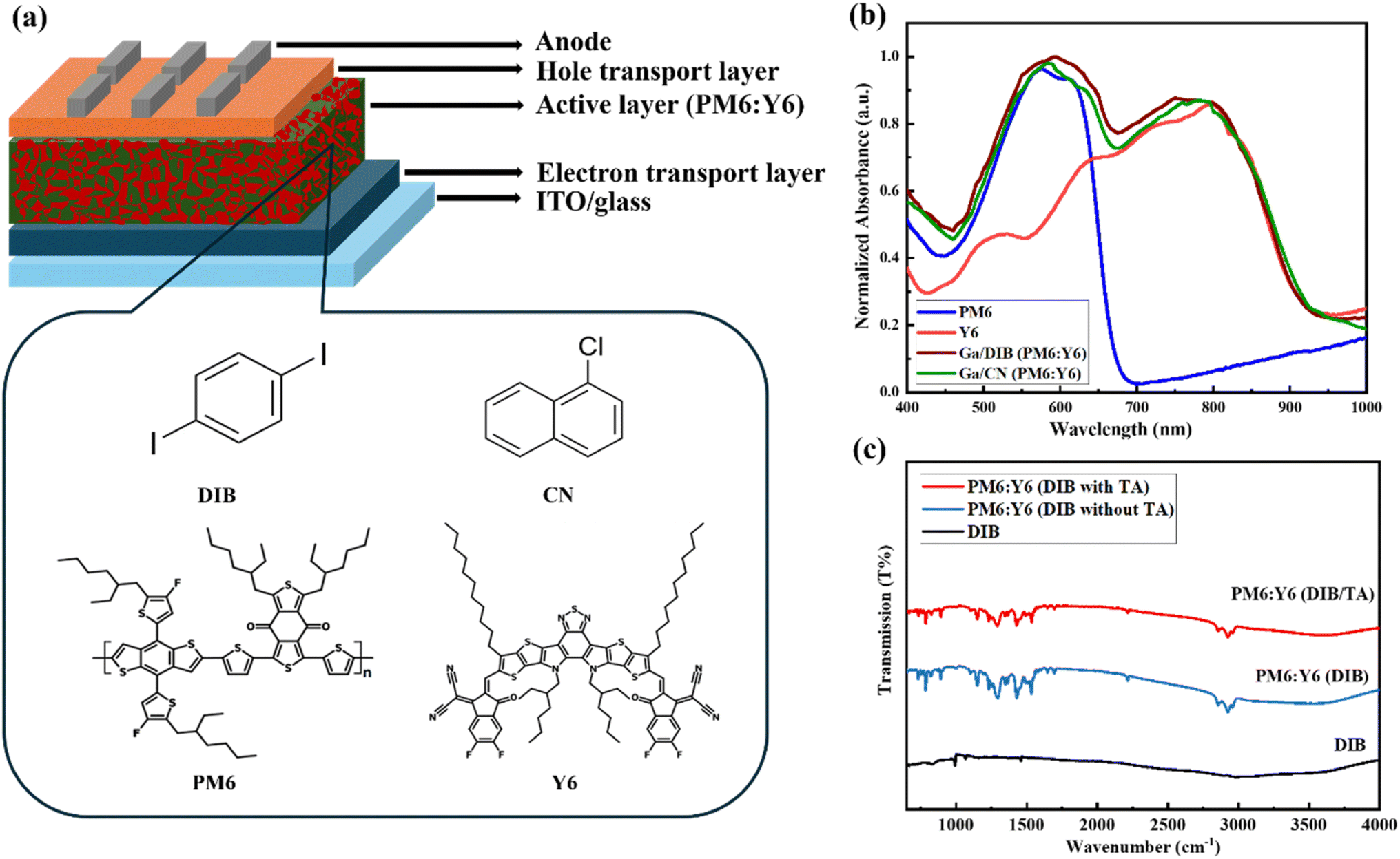 | ||
| Fig. 1 (a) Schematic diagram of the inverted device structure of non-fullerene OSCs, and chemical structures of additives, donor materials, and acceptor materials (b) absorption spectra of PM6, Y6, Ga/DIB (PM6:Y6) and Ga/CN (PM6:Y6). (c) Fourier transform infrared spectroscopy (FTIR) transmission spectra of DIB with and without thermal annealing. | ||
Fourier transform infrared spectroscopy (FTIR) measurements were used to provide stronger evidence that DIB was evaporated in the PM6:Y6 blend without undergoing thermal annealing (TA) treatment. Fig. 1c shows the FTIR spectra of the DIB solid additive and PM6:Y6 (DIB) active layer with and without thermal annealing films. The peaks associated with the DIB vanished in the FTIR spectra of the PM6:Y6 (DIB) blend film when thermal annealing (TA) was not performed. The FTIR results indicated that the DIB was completely evaporated from the active layer. Similarly, the PM6:Y6 (CN) active layer film regardless of whether it was treated with TA or not, had distinct peaks of CN at 765 cm−1, as seen in Fig. S1 of the ESI.† These findings indicate that there was still a tiny quantity of CN present in the active layer, and it was challenging to completely eliminate it using the TA approach.39
As seen in Fig. 1a, the OSCs were processed using an inverted device structure made of indium tin oxide (ITO) glass/ZnO/PM6:Y6/MoO3/Ag. The ESI† explains the device's fabrication process, including the chemical details and the characterisation formula. It was discovered that the ideal concentration of the additive DIB was 12 mg mL−1, whereas the ideal concentration of gallium in ZnO was found to be 6%. The utilization of ZnO as an ETL with the inclusion of the solvent additive CN and the solid additive DIB, also known as devices D1 and D3, was examined in this work. Additionally, the D2 and D4 devices, with the addition of CN and DIB, respectively, correspond to GZO ETL. The J–V characteristics of the best PM6:Y6 devices, with or without the solid additive DIB, are shown in Fig. 2a. Table 1 shows the parameters of the devices that are related to each other. The films that developed by combining PM6 and Y6, then subjected to CN treatment, had a maximum PCE of 14.94%. These films also had an open-circuit voltage (Voc) of 0.82 V, a short-circuit current (Jsc) of 26.43 mA cm−2, and a (FF) of 68.44%. These values are similar to those published in the literature.27 In addition, the efficiency of the devices improved when utilized GZO ETL compared to ZnO ETL. As a result, the devices with CN additive achieved an efficiency of 16.08%. The application of 1,4-DIB resulted in a notable PCE of 16.67%, accompanied by a voltage open circuit (Voc) of 0.82 V. Additionally, there was an improvement in the short-circuit (Jsc) to 28.88 mA cm−2, and a large rise in the (FF) to 71.92%. Thermal annealing and other post-treatments were not used in this case.
 | ||
| Fig. 2 (a) Current density versus voltage (J–V) characteristics of the best-performed devices based on PM6:Y6 with solvent additive CN and solid additive DIB. (b) EQE spectra of PM6:Y6 with solvent additive CN and solid additive DIB [here, ZnO as an electron transport layer (ETL) with the addition of the solvent additive CN and the solid additive DIB, referred to as devices D1 and D3. Also, devices D2 and D4 correspond to GZO ETL with the addition of CN and DIB, respectively]. | ||
| Devices | PCE (%) | V oc (V) | J sc (mA cm−2) | FF (%) |
|---|---|---|---|---|
| D1-ZnO/PM6:Y6 (CN) | 14.94 | 0.82 | 26.43 | 68.44 |
| D2-Ga:ZnO/PM6:Y6 (CN) | 15.43 | 0.82 | 26.62 | 69.13 |
| D3-ZnO/PM6:Y6 (DIB) | 16.08 | 0.82 | 27.76 | 69.88 |
| D4-Ga:ZnO/PM6:Y6 (DIB) | 16.67 | 0.82 | 28.88 | 71.92 |
We measured the external quantum efficiency (EQE) of the best-performing devices with and without 1,4-DIB in order to confirm the Jsc, as Fig. 2b illustrates. The EQE between 400 and 700 nm is mostly influenced by PM6, whereas the EQE between 700 and 950 nm is predominantly affected by Y6. In comparison to devices with ZnO ETL, those treated with DIB and GZO as the ETL exhibited improved EQE in the 450–900 nm wavelength range. Values obtained from the integration of the EQE spectra closely matched the measured values. Furthermore, the UV-vis absorption of the PM6:Y6 blended films is shown in Fig. 1b. It is noteworthy to notice that PM6 and Y6 are responsible for the two peaks that appear at 610 nm and 815 nm, respectively. It is anticipated that the addition of DIB to the PM6:Y6 mix film increased the absorption peak. This increase could be ascribed to the enhanced stacking of Y6 molecules, compatible with the EQE data.40 We investigated UV-vis spectroscopy on various concentrations of Ga doping in the ETL and presented the resultant Tauc plot in Fig. S2† for pure ZnO-based ETL and at 6%Ga doped ZnO ETL. The measured bandgap for pure ZnO and 6%Ga doped ZnO were 3.34 eV and 3.38 eV respectively. Due to the Burstein–Moss effect, and the additional electron generated when the Zn2+ ion in the ZnO lattice is replaced by Ga3+, the bandgap improvement in the 6%Ga doped ZnO layer causes an increase in charge carrier concentrations.41 Furthermore, Fig. S3† illustrates the X-ray diffraction (XRD) patterns of both the ZnO and the Ga-doped ETL. The XRD patterns show a complete match between the observed diffraction peaks with the hexagonal wurtzite structure of ZnO, indicating that Ga has completely replaced Zn in the ZnO lattice.
Furthermore, to gain insight into the surface chemical bonding of the films of ZnO and GZO with XPS spectra has also been examined, as shown in Fig. S4.† The XPS survey spectra of the samples confirms the existence of O, Zn, and/or Ga elements which proves that Ga is incorporated in the film. In the XPS spectra of the GZO ETLs, the peaks at 1118 eV and 1144 eV correspond to the electronic states of Ga 2p3/2 and Ga 2p1/2, respectively. The Ga peaks in the GZO film indicate the successful doping of Ga atoms into the ZnO lattices.42
The work function of ZnO ETL and GZO ETL were measured by ultraviolet photoelectron spectroscopy (UPS) (Fig. S5†). He I (21.2 eV) was utilized as a photon source for the UPS measurement. The work function, an essential surface property, governs the formation of the Schottky barrier for non-ohmic connections and the degree of charge transfer between the organic layer and the transparent conductive oxide. The measured work functions for ZnO ETL and GZO ETL are 4.18 and 4.02, respectively. The decrease in the work function (WF) of the GZO ETL can promote a more efficient energy level alignment within the solar cell and improve charge extraction. Therefore, the Jsc of the GZO devices 28.88 mA cm−2 is much higher than the Jsc of the ZnO-based devices 26.43 mA cm−2.6,43
To assess the efficacy of DIB in devices, we developed twenty devices that were treated with CN and DIB. We then prepared a statistical distribution diagram to visualize the fluctuations in Voc, Jsc, FF, and PCE, as shown in Fig. S6a–d.† In terms of device parameters, the devices that were treated with DIB showed the most remarkable outcomes, as shown in Fig. S6a–d.† Therefore, the utilization of DIB in OSCs contributed to significant uniformity and helped reduce variations across various batches.
2.2. The charge transport, recombination, and extraction properties of the devices
Fig. 3a depicts the J–V curves of devices based on CN and DIB additives under dark conditions. The intersection of the dark J–V curve with the y-axis under reverse bias indicates the leakage current of the device.44 It suggested that devices based on DIB can result in improved charge transportation and limited charge recombination for devices based on GZO ETL.45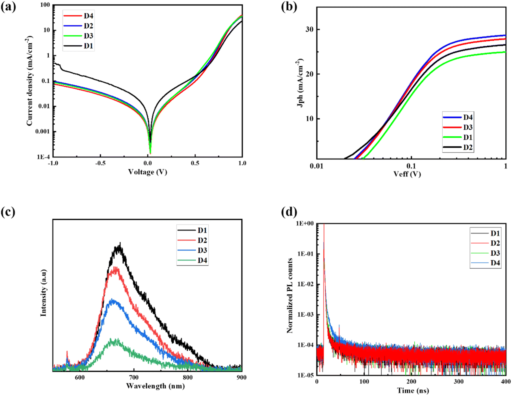 | ||
| Fig. 3 (a) Dark current–voltage characteristics of the fabricated solar cells for CN and DIB-based devices. (b) Variations of photocurrent (Jph) with an effective bias voltage (Veff) in OSCs for CN and DIB-based devices with different ETL. (c and d) PL and TRPL spectra for CN and DIB-based devices with different ETL. | ||
The photoluminescence (PL) intensity is closely correlated with the Jsc value of the solar cell. A high PL intensity signifies the presence of a significant number of excitons in the active layer.46,47 PL quenching refers to the reduction in PL intensity that happens when excitons are effectively separated.48,49 A higher PL intensity indicates a less effective charge dissociation process. In this experiment, the highest PL intensity of the films showed a substantial increase when compared to films treated with ZnO ETL. Fig. 3c demonstrates that the films treated with CN and DIB for the ETL comprising GZO exhibit a negligible increase in the PL intensity. This results indicates that the devices treated with CN and DIB show an inadequate charge dissociation process in ZnO ETL-based devices, however, this is not true for GZO ETL-based devices. Fig. 3c demonstrates that the device exposed to DIB and GZO treatment exhibited the least PL intensity. The primary factor responsible for the decline in Jsc in CN-based devices is their reduced capacity to dissociate excitons. The addition of the DIB solid additive to the PM6:Y6 blend enhances the carrier's effective lifetime, as seen by the TrPL in Fig. 3d.
We conducted a charge extraction possibility (P) study for devices based on CN and DIB additives for both with/without modified ETLs by combining J–V characterisation and dark J–V measurement. The research focuses on two main parameters: photocurrent density (Jph) and effective voltage (Veff). Fig. 3b depicts the basic correlation between the Jph and the Veff. The Jph is the quantitative measure of the difference between the photocurrent density observed under illumination conditions (JL) and the photocurrent density observed under dark conditions (JD). The equation to compute the effective voltage (Veff) is Veff = Voc − Vapp, where Voc represents the compensating voltage when Jph is equal to zero, and Vapp is the applied voltage.50 In order to calculate the charge collection probability Pdiss, we standardized the values of Jph and Jsat. The term “Jsat” refers to the saturation current, which signifies the complete separation and conversion of all generated excitons into free charge carriers. These carriers are then transferred and accumulated at either the positive or negative electrode of the device. The results showed that the devices treated with DIB had a higher Pdiss value of 97.5%, while the CN-based devices had a value of 96.6% under short-circuit conditions (Veff = Voc). The improved photovoltaic performance of the devices based on DIB can be due to the combined effects of reduced recombination, balanced and increased mobilities, and greater charge-collecting efficiency.
To do a more comprehensive investigation of the electrical properties of the device, capacitance–voltage (C–V) measurements were conducted on both CN and DIB-based devices. Fig. 4b exhibits the Mott Schottky (MS) diagrams for devices utilizing CN and DIB additives, measured at a frequency of 100 kHz.51 Through the analysis of the MS plots, we can calculate the built-in potential (Vbi) by locating the point at which the curve meets the x-axis. The value of Vbi directly affects the voltage and charge transfer properties of the device. Inadequate Vbi commonly leads to subpar performance in organic solar cells. When the device is biased in the forward direction, if the applied voltage is greater than the Vbi value, the overall electrical field within the device will change direction, which will impede the movement and transfer of charges.52,53 It is clear that when the rise happened, the Vbi of the DIB-based device showed a steadily increasing trend in comparison to the other devices. Utilizing the solid additive DIB can enhance the Vbi of the gadget, elevating it from 0.67 V to 0.85 V. The observed variance in the built-in voltage (Vbi) remains consistent across all device types, as evidenced by the Voc values derived from the J–V characterization.
 | ||
| Fig. 4 (a) Impedance analysis of the best-performed devices based on PM6:Y6 with solvent additive CN and solid additive DIB. (b) Capacitance–voltage plot of PM6:Y6 with solvent additive CN and solid additive DIB. | ||
Electrochemical impedance spectroscopy (EIS) was used to further investigate the electrical properties of the devices by introducing solid additive DIB. Fig. 4a displays the Nyquist plots of the CN and DIB-treated devices with ZnO and Ga:ZnO-based ETL. The fitted equivalent circuit model reveals that the starting points in Nyquist plots represent the internal series resistance (RS), while the sizes of the semicircles show the values of the charge transfer resistance (RCT) in devices. Both the CN and DIB-processed devices display minor series resistance (RS) when using GZO ETL. However, the device treated with DIB shows better charge transport characteristics compared to CN-based devices (Table ST1†), which aligns with the enhanced FF and Jsc.6,54,55
2.3. The morphology of the active layer
Films surface morphology plays a crucial role in determining the performance of OSCs. Atomic force microscopy (AFM) and scanning electron microscopy (SEM) characterization were carried out to understand the effect of DIB and GZO on the film surface. The enhanced crystallinities of the GZO and DIB based active layer films surface have been observed from the SEM and AFM images. SEM studies indicate that a well-connected network can yield qualitative insights into the crystallinity of the BHJ film. The root mean square (RMS) surface roughness first decreases until it reaches a specific doping concentration, at which point it starts to increase. The finding is consistent with the SEM images in Fig. S7,† which show that the grain sizes grow as the Ga doping concentration increases. This helps create a smooth network that is crucial for the efficient flow of electric charge.10,56,57 Further to understand the effect of DIB on the surface morphology of the film, AFM measurements were carried out.58,59 Then, we investigated the films developed from CN and DIB using a GZO ETL. The correlation between the DIB solid additive and PM6:Y6 blends is illustrated by the notable enhancement in the aggregation morphology and the increased Rq value of the DIB film, as observed in Fig. 5 and Table 2, respectively. The films based on CN have a comparable pattern but are less pronounced than the ones based on DIB. Upon the formation of the blend film, the application of solid additive DIB treatment enhances the vertical phase alignment of the surface morphology (Fig. 5). We predict that DIB interacts with the materials in the active layer and affects the process of crystallization and molecular packing. | ||
| Fig. 5 Atomic force microscopy (AFM) images of PM6:Y6 with solvent additive CN and solid additive DIB-based films respectively. | ||
| Additive | R rms (nm) | Average (nm) |
|---|---|---|
| CN | 1.915 | 9.51 |
| DIB | 2.213 | 9.71 |
The utilization of GZO ETL and DIB may effectively inhibit the excessive self-aggregation of the Y6 molecule, hence preventing inadequate phase separation and oversized domains in the active layer film. Based on our findings, we predicted that the active layer film experiences a molecular arrangement optimization throughout the post-treatment process, particularly when removing the DIB solid additive. This optimization results in a well-organized phase separation inside the active layer.60,61 Hence, the incorporation of both Ga in ZnO ETL and DIB additives in the PM6:Y6 active layer film guarantees an enhanced PCE in organic solar cells, as shown by PL data.
2.4. The stability of the devices
The stability of OSCs is a critical factor that must be addressed for successful commercialization. Hence, it is important to elucidate the variables that impact the efficiency of solar cells and the longevity of the devices. In this case, the effectiveness is reduced when using both CN and DIB-based devices. Fig. 6 demonstrates that the devices treated with DIB exhibit good stability when placed in a glovebox filled with N2. After 30 days of storage, the devices retained 92% of their initial efficiency. Similar to the PCE, other photovoltaic parameters such as Jsc, Voc, and FF also exhibit good stability in DIB-treated devices compared to CN-based devices. The initial decline in photovoltaic performance for both CN and DIB-based systems was attributed to burn-in degradation.44 | ||
| Fig. 6 Normalised PCE for CN and DIB-based devices with GZO ETL with time. | ||
To present the extensive application of volatile solid additives in improving photovoltaic performance, we employed DIB additive in a different combination containing non-fullerene PTB7-Th:IEICO-4F (D/A) active layer. The J–V curves are illustrated in Fig. S8,† and the corresponding device parameters are provided in Table ST2.† The device achieved an approximate PCE of 11% using a binary blend of PTB7-Th and IEICO-4F. Furthermore, the stability of the devices associated with the DIB solid additive was evaluated, as seen in Fig. S9.† The DIB solid additive treated devices exhibit superior power conversion efficiency, as well as better (FF) and photostability, in comparison to the equivalent CN-processed devices. The results suggest that the DIB solid additive, which is extremely volatile, has the ability to be a versatile solid additive for improving the solar efficiency of OSCs.
Therefore, we propose that the halogen bond established between the iodine atom in DIB and the cyano group in Y6 should be considered as the intrinsic catalyst for enhancing denser molecular stacking and a more structured molecular arrangement in the mutually advantageous interpenetrating donor/acceptor domains. Owing to its suitable volatility, the residual DIB residue could be removed without requiring a thermal annealing procedure, leading to an ideal morphology and efficient molecular arrangement. This leads to a notable enhancement in performance compared to CN based devices. DIB also exhibits greater tolerance to variations in concentration, which is advantageous for ensuring the repeatability and industrial applicability of the device.
3. Conclusion
To summarize, we effectively included Ga-doped ZnO as an electron transport layer and solid additive DIB into binary devices, resulting in high-performance non-fullerene OSCs. The blend of PM6:Y6 treated with DIB, together with GZO ETL, exhibited better and well-balanced mobility, reduced charge recombination, and effective charge extraction. These enhancements can be attributed to the improved morphology of the film. The superior performance of the PM6:Y6-based devices was attributed to their improved crystallinity and molecular packing, as seen by their slightly higher Jsc (28.88 mA cm−2), greatly enhanced FF (71.92%), and much better PCE (16.67%) compared to 14.94% for the control device. The devices developed with DIB exhibit exceptional repeatability and stability, omitting the requirement for thermal annealing in PM6:Y6-based OSCs. Incorporating DIB additive into the active layer is a simple but highly efficient approach to improve OSC performances and paves the way for further additive advancements.Data availability
All relevant data are within the manuscript and its ESI.†Conflicts of interest
The authors declare no conflict of interest.Acknowledgements
This study was funded by the Discovery Project (DP210100904) of the Australian Research Council (ARC). The authors express their gratitude for the constant support provided by the personnel of the Photovoltaic and Renewable Energy Engineering School, the Electron Microscope Unit, and the Solid State and Elemental Analysis Unit in the Mark Wainwright Analytical Centre at the University of New South Wales.References
- X. Li, F. Pan, C. Sun, M. Zhang, Z. Wang, J. Du, J. Wang, M. Xiao, L. Xue, Z.-G. Zhang, C. Zhang, F. Liu and Y. Li, Nat. Commun., 2019, 10, 519 CrossRef CAS PubMed.
- S. Juillard, E. Planes, M. Matheron, L. Perrin, S. Berson and L. Flandin, ACS Appl. Mater. Interfaces, 2018, 10, 29805–29813 CrossRef CAS PubMed.
- R. Bashir, M. Kashif Bilal, A. Bashir, J. Zhao, S. Ullah Asif, W. Ahmad, J. Xie and W. Hu, Nanoscale, 2021, 13, 12991–12999 RSC.
- J. Dong, J. Guo, X. Wang, P. Dong, Z. Wang, Y. Zhou, Y. Miao, B. Zhao, Y. Hao, H. Wang, B. Xu and S. Yin, ACS Appl. Mater. Interfaces, 2020, 12, 46373–46380 CrossRef CAS PubMed.
- L. Chang, M. Sheng, L. Duan and A. Uddin, Org. Electron., 2021, 90, 106063 CrossRef CAS.
- M. B. Upama, N. K. Elumalai, M. A. Mahmud, C. Xu, D. Wang, M. Wright and A. Uddin, Sol. Energy Mater. Sol. Cells, 2018, 187, 273–282 CrossRef CAS.
- C. Chen, L. Wang, W. Xia, K. Qiu, C. Guo, Z. Gan, J. Zhou, Y. Sun, D. Liu, W. Li and T. Wang, Nat. Commun., 2024, 15, 6865 CrossRef CAS PubMed.
- Y. Sun, L. Wang, C. Guo, J. Xiao, C. Liu, C. Chen, W. Xia, Z. Gan, J. Cheng, J. Zhou, Z. Chen, J. Zhou, D. Liu, T. Wang and W. Li, J. Am. Chem. Soc., 2024, 146, 12011–12019 CrossRef CAS PubMed.
- W. B. Tarique and A. Uddin, Mater. Sci. Semicond. Process., 2023, 163, 107541 CrossRef CAS.
- W. B. Tarique, M. H. Rahaman, S. S. Dipta, A. H. Howlader and A. Uddin, Nanomanufacturing, 2024, 4, 81–98 CrossRef.
- J. Sun, S. Yu, Q. Zheng, S. Cheng, X. Wang, H. Zhou, Y. Lai and J. Yu, J. Mater. Sci.: Mater. Electron., 2017, 28, 2272–2278 CrossRef CAS.
- N. Zhou, X. Guo, R. P. Ortiz, S. Li, S. Zhang, R. P. H. Chang, A. Facchetti and T. J. Marks, Adv. Mater., 2012, 24, 2242–2248 CrossRef CAS PubMed.
- J. Huang, Z. Yin and Q. Zheng, Energy Environ. Sci., 2011, 4, 3861–3877 RSC.
- M. A. Mahmud, N. K. Elumalai, M. B. Upama, D. Wang, K. H. Chan, M. Wright, C. Xu, F. Haque and A. Uddin, Sol. Energy Mater. Sol. Cells, 2017, 159, 251–264 CrossRef CAS.
- M. B. Upama, N. K. Elumalai, M. A. Mahmud, M. Wright, D. Wang, C. Xu, F. Haque, K. H. Chan and A. Uddin, Appl. Surf. Sci., 2017, 416, 834–844 CrossRef CAS.
- S. K. Swami, N. Chaturvedi, A. Kumar, V. Kumar, A. Garg and V. Dutta, Sol. Energy, 2022, 231, 458–463 CrossRef CAS.
- P. R. Berger and M. Kim, J. Renewable Sustainable Energy, 2018, 10, 013508 CrossRef.
- C. Yan, S. Barlow, Z. Wang, H. Yan, A. K.-Y. Jen, S. R. Marder and X. Zhan, Nat. Rev. Mater., 2018, 3, 18003 CrossRef CAS.
- G. Chai, Y. Chang, J. Zhang, X. Xu, L. Yu, X. Zou, X. Li, Y. Chen, S. Luo, B. Liu, F. Bai, Z. Luo, H. Yu, J. Liang, T. Liu, K. S. Wong, H. Zhou, Q. Peng and H. Yan, Energy Environ. Sci., 2021, 14, 3469–3479 RSC.
- Q. An, J. Wang, X. Ma, J. Gao, Z. Hu, B. Liu, H. Sun, X. Guo, X. Zhang and F. Zhang, Energy Environ. Sci., 2020, 13, 5039–5047 RSC.
- R. Sorrentino, E. Kozma, S. Luzzati and R. Po, Energy Environ. Sci., 2021, 14, 180–223 RSC.
- J. Singh, M. Narayan, D. Ompong and F. Zhu, J. Mater. Sci.: Mater. Electron., 2017, 28, 7095–7099 CrossRef CAS.
- W. Kim, J. K. Kim, E. Kim, T. K. Ahn, D. H. Wang and J. H. Park, J. Phys. Chem. C, 2015, 119, 5954–5961 CrossRef CAS.
- X. Xu, T. Yu, Z. Bi, W. Ma, Y. Li and Q. Peng, Adv. Mater., 2018, 30, 1703973 CrossRef PubMed.
- J. Fu, P. W. K. Fong, H. Liu, C.-S. Huang, X. Lu, S. Lu, M. Abdelsamie, T. Kodalle, C. M. Sutter-Fella, Y. Yang and G. Li, Nat. Commun., 2023, 14, 1760 CrossRef CAS PubMed.
- W. Xu, M. Zhang, J. Xiao, M. Zeng, L. Ye, C. Weng, B. Zhao, J. Zhang and S. Tan, Polym. Chem., 2020, 11, 6178–6186 RSC.
- J. Yuan, Y. Zhang, L. Zhou, G. Zhang, H.-L. Yip, T.-K. Lau, X. Lu, C. Zhu, H. Peng, P. A. Johnson, M. Leclerc, Y. Cao, J. Ulanski, Y. Li and Y. Zou, Joule, 2019, 3, 1140–1151 CrossRef CAS.
- S. Dai, S. Chandrabose, J. Xin, T. Li, K. Chen, P. Xue, K. Liu, K. Zhou, W. Ma, J. M. Hodgkiss and X. Zhan, J. Mater. Chem. A, 2019, 7, 2268–2274 RSC.
- M. Li, K. Gao, X. Wan, Q. Zhang, B. Kan, R. Xia, F. Liu, X. Yang, H. Feng, W. Ni, Y. Wang, J. Peng, H. Zhang, Z. Liang, H.-L. Yip, X. Peng, Y. Cao and Y. Chen, Nat. Photonics, 2017, 11, 85–90 CrossRef CAS.
- W. Yang, Z. Luo, R. Sun, J. Guo, T. Wang, Y. Wu, W. Wang, J. Guo, Q. Wu, M. Shi, H. Li, C. Yang and J. Min, Nat. Commun., 2020, 11, 1218 CrossRef CAS PubMed.
- D. Yang, F. C. Löhrer, V. Körstgens, A. Schreiber, S. Bernstorff, J. M. Buriak and P. Müller-Buschbaum, ACS Energy Lett., 2019, 4, 464–470 CrossRef CAS.
- Y. Jiang and Z. Li, Synth. Met., 2023, 299, 117480 CrossRef CAS.
- Y.-F. Ma, Y. Zhang and H.-L. Zhang, J. Mater. Chem. C, 2022, 10, 2364–2374 RSC.
- Z. Gan, L. Wang, J. Cai, C. Guo, C. Chen, D. Li, Y. Fu, B. Zhou, Y. Sun, C. Liu, J. Zhou, D. Liu, W. Li and T. Wang, Nat. Commun., 2023, 14, 6297 CrossRef CAS PubMed.
- T. Chen, Y. Bai, X. Ji, W. Feng, T. Duan, X. Jiang, Y. Yi, J. Yu, G. Lu, X. Wan, B. Kan and Y. Chen, Nano Energy, 2024, 125, 109604 CrossRef CAS.
- Y. Chen, C. Han, X. Xia, L. Yu, X. Guo and M. Zhang, Org. Electron., 2024, 125, 106975 CrossRef CAS.
- Z.-C. Wen, H. Yin and X.-T. Hao, Surf. Interfaces, 2021, 23, 100921 CrossRef CAS.
- J. Yang, X. Wang, X. Yu, J. Liu, Z. Zhang, J. Zhong and J. Yu, Nanomaterials, 2023, 13, 2899 CrossRef CAS PubMed.
- Y. Xie, H. S. Ryu, L. Han, Y. Cai, X. Duan, D. Wei, H. Y. Woo and Y. Sun, Sci. China:Chem., 2021, 64, 2161–2168 CrossRef CAS.
- S. Shoaee, H. M. Luong, J. Song, Y. Zou, T.-Q. Nguyen and D. Neher, Adv. Mater., 2024, 36, 2302005 CrossRef CAS PubMed.
- K. G. Saw, N. M. Aznan, F. K. Yam, S. S. Ng and S. Y. Pung, PLoS One, 2015, 10, e0141180 CrossRef CAS PubMed.
- A. Khorsand Zak, N. S. Abd Aziz, A. M. Hashim and F. Kordi, Ceram. Int., 2016, 42, 13605–13611 CrossRef CAS.
- H. W. Lee, S. Biswas, H. Choi, Y. Lee and H. Kim, Appl. Surf. Sci., 2024, 659, 159930 CrossRef CAS.
- L. Duan, M. Guli, Y. Zhang, H. Yi, F. Haque and A. Uddin, Energy Technol., 2020, 8, 1901401 CrossRef CAS.
- M. F. Albab, M. Jahandar, Y. H. Kim, Y.-K. Kim, M. Shin, A. Prasetio, S. Kim and D. C. Lim, Nano Energy, 2024, 121, 109219 CrossRef CAS.
- S. Siebentritt, T. P. Weiss, M. Sood, M. H. Wolter, A. Lomuscio and O. Ramirez, J. Phys.: Mater., 2021, 4, 042010 CAS.
- K. Öğütman, K. O. Davis, E. Schneller, V. Yelundur and W. V. Schoenfeld, Sol. Energy, 2017, 158, 869–874 CrossRef.
- X. Geng, Y. Liu, X. Zou, E. M. J. Johansson and J. Sá, Phys. Chem. Chem. Phys., 2023, 25, 22607–22613 RSC.
- L. Benatto, M. de J. Bassi, L. C. W. de Menezes, L. S. Roman and M. Koehler, J. Mater. Chem. C, 2020, 8, 8755–8769 RSC.
- P. W. M. Blom, V. D. Mihailetchi, L. J. A. Koster and D. E. Markov, Adv. Mater., 2007, 19, 1551–1566 CrossRef CAS.
- N. Tokmoldin, C. Deibel, D. Neher and S. Shoaee, Adv. Energy Mater., 2024, 14, 2401130 CrossRef CAS.
- Y. Wang, Q. Chen, Z. Liu, F. Yu, W. Su, Z. Cai, W. Guan, Y. Li, L. Sheng, Z. Qi, E. Wang and L. Hou, Chem. Eng. J., 2023, 452, 139479 CrossRef CAS.
- O. Almora, C. Aranda, E. Mas-Marzá and G. Garcia-Belmonte, Appl. Phys. Lett., 2016, 109, 173903 CrossRef.
- F. Igbari, M. Li, Y. Hu, Z.-K. Wang and L.-S. Liao, J. Mater. Chem. A, 2016, 4, 1326–1335 RSC.
- L. Duan, Y. Zhang, M. He, R. Deng, H. Yi, Q. Wei, Y. Zou and A. Uddin, ACS Appl. Mater. Interfaces, 2020, 12, 27433–27442 CrossRef CAS PubMed.
- M. Thambidurai, J. Y. Kim, J. Song, Y. Ko, H. Song, C. Kang, N. Muthukumarasamy, D. Velauthapillai and C. Lee, J. Mater. Chem. C, 2013, 1, 8161–8166 RSC.
- J. You, C.-C. Chen, L. Dou, S. Murase, H.-S. Duan, S. A. Hawks, T. Xu, H. J. Son, L. Yu, G. Li and Y. Yang, Adv. Mater., 2012, 24, 5267–5272 CrossRef CAS PubMed.
- X. Zhu, B. Guo, J. Fang, T. Zhai, Y. Wang, G. Li, J. Zhang, Z. Wei, S. Duhm, X. Guo, M. Zhang and Y. Li, Org. Electron., 2019, 70, 25–31 CrossRef CAS.
- R. Yu, H. Yao, L. Hong, Y. Qin, J. Zhu, Y. Cui, S. Li and J. Hou, Nat. Commun., 2018, 9, 4645 CrossRef PubMed.
- J. Qin, Q. Yang, J. Oh, S. Chen, G. O. Odunmbaku, N. A. N. Ouedraogo, C. Yang, K. Sun and S. Lu, Adv. Sci., 2022, 9, e2105347 CrossRef PubMed.
- J. Fu, H. Chen, P. Huang, Q. Yu, H. Tang, S. Chen, S. Jung, K. Sun, C. Yang, S. Lu, Z. Kan, Z. Xiao and G. Li, Nano Energy, 2021, 84, 105862 CrossRef CAS.
Footnote |
| † Electronic supplementary information (ESI) available. See DOI: https://doi.org/10.1039/d4se01240b |
| This journal is © The Royal Society of Chemistry 2025 |