
 Open Access Article
 This Open Access Article is licensed under a
 Creative Commons Attribution 3.0 Unported Licence
Pt-free MoS2 co-catalyst enables record photocurrent density in Sb2Se3 photocathodes for highly efficient solar hydrogen production†
Munir
Ahmad
 a,
Anadil
Gul
b,
Hafiz Sartaj
Aziz
a,
Tahir
Imran
a,
Muhammad
Ishaq
a,
Muhammad
Abbas
a,
Zhenghua
Su
a and
Shuo
Chen
*a
a,
Anadil
Gul
b,
Hafiz Sartaj
Aziz
a,
Tahir
Imran
a,
Muhammad
Ishaq
a,
Muhammad
Abbas
a,
Zhenghua
Su
a and
Shuo
Chen
*a
aInstitute of Thin Film Physics and Applications, Shenzhen Key Laboratory of Advanced Thin Films and Applications, Key Laboratory of Optoelectronic Devices and Systems of Ministry of Education and Guangdong Province, State Key Laboratory of Radio Frequency Heterogeneous Integration, College of Physics and Optoelectronic Engineering, Shenzhen University, Shenzhen, 518060, China. E-mail: chensh@szu.edu.cn
bCollege of Health Science and Environmental Engineering, Shenzhen Technology University, Shenzhen, 518118, China
First published on 16th April 2025
Abstract
Antimony selenide (Sb2Se3) emerges as a potential light-absorbing material for thin film photovoltaics and photoelectrochemical (PEC) water-splitting devices, due to its earth-abundant constituents and excellent photoelectric properties. However, losses caused by corrosion and sluggish charge transfer at the semiconductor/electrolyte interface require a co-catalyst to enhance these kinetic factors. In this study, MoS2 is employed as a cost-effective, noble-metal-free catalyst to enhance the photocurrent density (Jph), half-cell solar-to-hydrogen (HC-STH) conversion efficiency and stability of Sb2Se3-based photocathodes. Optimized thermodynamic/kinetic physical vapor deposition of MoS2 substantially improves PEC performance, resulting champion Mo/Sb2Se3/CdS/MoS2 photocathode that achieves a record Jph of 31.03 mA cm−2 at 0 VRHE and the highest HC-STH efficiency of 3.08%, along with stability for over 5 hours in an acidic (pH 1) buffer solution. It is systematically revealed that MoS2 reduces the photo-corrosion effect, decreases electron–hole recombination, and provides a significant increase in charge transfer efficiency at the semiconductor/electrolyte interface. This work highlights the potential of cost-effective, high-performance Sb2Se3-based photocathodes in advancing efficient PEC devices for solar hydrogen production.
1. Introduction
Hydrogen production by solar-driven water splitting in photoelectrochemical (PEC) devices is one of the most attractive strategies to convert clean and abundant radiation into non-polluting and storable chemical fuels.1 Hydrogen energy is a carbon-free fuel that can be used in various industries, transportation, and heating applications. Currently, burning fossil fuels produces the majority of hydrogen, which leads to serious carbon emission problems.2 Production of green hydrogen energy through sunlight harvesting is a highly efficient approach for overcoming worldwide environmental problems and energy shortages; however, it remains challenging.3 Recently, different research groups have focused on introducing new photocatalysts or advanced methods to produce hydrogen energy through water splitting. Among these technologies, PEC solar water splitting is a clean, sustainable, and cost-effective, technique to produce hydrogen from solar irradiation.4 Some well-studied oxides, for example, CuFeO25 and Cu2O,6 and different chalcogenides like CuInS2,7 CuGaSe2,8 and CuIn1−xGaxSe2 (ref. 9 and 10) as well as newly emerging materials like Cu2ZnSn(S,Se)4,2 Cu2BaSn(S,Se)4![[thin space (1/6-em)]](https://www.rsc.org/images/entities/char_2009.gif) 11 and Sb2Se3 12–14 are studied as photocathode materials.
11 and Sb2Se3 12–14 are studied as photocathode materials.
Among the materials for hydrogen production, Sb2Se3 has emerged as an excellent light-absorbing material for PEC applications because of its earth-abundant elements, low-cost, eco-friendly, high absorption coefficient (>105 cm−1), suitable bandgap (∼1.2 eV), and remarkable photoelectric properties. Additionally, Sb2Se3 exhibits intrinsic stability in neutral and acidic electrolytes, with negligible self-reduction or photo-corrosion, making it a suitable material for efficient PEC photocathodes.15 Despite these advantages, Sb2Se3-based photocathodes face many challenges such as surface corrosion caused by multiple functional layers, electron–hole non-radiative recombination caused by defects, and sluggish charge transfer at the semiconductor/electrolyte interface, which limit their PEC efficiency and long-term stability. To address these challenges, employing a suitable co-catalyst on the photocathode surface is very important. Noble metals like platinum (Pt) have been widely used as co-catalysts in Sb2Se3-based photocathodes, but their high cost and rare availability limit their commercial applications.16,17 Hence, the search for cost-effective and non-toxic alternative co-catalysts is highly desirable for developing efficient Sb2Se3-based photocathodes.
Recently, the development of co-catalysts like metal alloys, carbides, phosphides, nitrides, borides, and chalcogenides for the representative hydrogen evolution reaction (HER) has made significant progress.18,19 Among them, molybdenum sulfide (MoS2) has gained attention as a promising noble-metal-free co-catalyst. As a transition metal dichalcogenide (TMD), MoS2 possesses a suitable 2D layered structure, excellent chemical stability, and favorable band alignment for inducing the HER.20,21 Additionally, amorphous MoS2 has a high concentration of active sites at the edge layers, which enhances its electrocatalytic activity as compared to the crystalline form.22 A solution-based approach to synthesize MoS2 (crystalline/amorphous) has been used in different photocathodes (e.g., Cu2O, Cu2ZnSnS4, and Sb2Se3).23,24 Actually, it still encounters challenges in terms of scalability, thickness uniformity, and composition variability.24 In contrast, physical vapor deposition (PVD) techniques, such as sputtering, provide a suitable preparation method for producing uniform, large-scale, and stable MoS2 thin film co-catalysts; however, this approach remains underexplored.25
This work started the preparation of eco-friendly Sb2Se3 light-harvesting films with favorable growth orientation and large crystal grains through an efficient combination reaction involving pre-sputtered and post-selenized Sb metallic precursors. After CdS buffer layer deposition, the binary compound MoS2 was sputtered as a co-catalyst instead of using noble-metal Pt, with a focus on MoS2 co-catalyst thickness engineering to enhance both light-harvesting efficiency and HER activity. In short, the introduction of optimized MoS2 could significantly alleviate the photo-corrosion effect, suppress charge carrier recombination loss, and reduce the charge transfer resistance at the semiconductor/electrolyte interface. Moreover, the MoS2 incorporation contributed to a favorable surface wettability with more reaction sites and favorable surface band bending with accelerated photoelectron transfer characteristics. As a result, the champion MoS2-modified Pt-free Sb2Se3 photocathode exhibited a record photocurrent density (Jph) of 31.03 mA cm−2 at 0 V versus the reversible hydrogen electrode (RHE, VRHE), and the highest half-cell solar-to-hydrogen (HC-STH) conversion efficiency of 3.08% in a pH 1 acid buffer solution. Furthermore, the device exhibited a significant improvement in long-term stability as compared to its Pt-involved counterpart. This work highlights the potential of PVD-processed MoS2 as a cost-effective and highly-efficient co-catalyst, advancing the development of efficient and stable Sb2Se3-based photocathodes for solar hydrogen production.
2. Experimental section
2.1. Preparation of Sb2Se3/CdS/MoS2 photocathodes
The Sb2Se3 light-absorbing layer and CdS buffer layer were sequentially deposited on a Mo-coated soda lime glass substrate according to our previously reported work.26 After the deposition of Sb2Se3 and CdS, the MoS2 layer with different thicknesses ranging from 20 to 40 nm was deposited as a co-catalyst by RF (radio frequency) magnetron sputtering using a MoS2 target. It was carried out with a 50 W sputtering power, an Ar gas flow of 50 sccm, and a working pressure of 2 Pa. The MoS2 layer thickness was controlled by sputtering deposition times of 400 s, 600 s, and 800 s, yielding 20, 30, and 40 nm MoS2 layers based on a 0.05 nm s−1 deposition rate, and the corresponding samples were labelled as M-20, M-30, and M-40 respectively. Finally, the Mo layer was exposed at the thin film edge to achieve a conductive back contact, and Ag colloids were deposited on its surface by thermal evaporation. The schematic of the synthesis process of glass/Mo/Sb2Se3/CdS/MoS2 photocathode is shown in Fig. S1 (ESI).†2.2. Characterization
The crystallinity of Sb2Se3-based photocathodes was studied by X-ray diffraction (XRD) using an Ultima-IV diffractometer with Cu Kα radiation. The morphologies of the surface, cross-section, and structure were acquired using a scanning electron microscope (SEM, Zeiss SUPRA 55) and the corresponding elemental composition was studied by using an energy dispersive spectroscope (EDS, BRUKER QUANTAX 200). The valence states of the involved elements were studied using X-ray photoelectron spectroscopy (XPS, Thermo Scientific ESCALAB 250Xi). In situ sputter etching was performed using a 10 kV Gas Cluster Ion Beam (GCIB) with a 6 × 6 mm2 surface treatment area during the XPS measurement. Atomic force microscopy (AFM) operated, via NT-MDT spectrum instruments in semi-contact mode, was used for the investigation of thin film morphology and surface roughness. Surface potential and topography characterization were further analyzed through a Kelvin probe force microscope (KPFM, Bruker Dimension ICON). Raman spectroscopy (Renishaw, InVia) was used for studying bonding information. PEC performance characterization was performed with an electrochemical workstation (CHI660e) under a three-electrode configuration, i.e., Ag/AgCl electrode as the reference electrode, Pt-wire as the counter electrode, and the as-fabricated photocathode as the working electrode. All tests were performed in acid electrolyte under simulated sunlight illumination (AM 1.5G) at a calibrated light intensity of 100 mW cm−2. Photoelectrochemical impedance spectroscopy (PEIS) was performed under simulated sunlight illumination in a 10−1 to 102 kHz frequency range at 0 VRHE. Mott–Schottky (M–S) experiments were performed in the dark using a 30 mV AC amplitude, scanning voltage between −0.5 and 0.1 V and a frequency of 104 Hz.3. Results and discussion
Mo/Sb2Se3/CdS/MoS2 thin-film photocathodes with different MoS2 co-catalyst loading amounts (i.e., 20 nm, 30 nm, and 40 nm) were prepared and studied; the corresponding devices were labelled as M-20, M-30, and M-40, respectively. Their PEC performance was measured using a classical 3-electrode PEC workstation, as shown in Fig. 1a. Upon light illumination, continuous visible hydrogen bubbles were observed on the photocathode surface, which migrated toward the acidic electrolyte (i.e., 0.5 M H2SO4), indicating the efficient HER through water splitting (Fig. 1b). The as-prepared Sb2Se3 photocathodes of area 2 × 2 cm2 were quasi-homogenous, as shown in Fig. 1b (inset), suggesting great potential in scalable applications. Before performing PEC measurements, a defined active area of 0.95 cm2 was exposed using a water-resistant, light-resistant glue to ensure accurate and reproducible performance evaluation. Generally, the thickness of both the light-absorbing layer (Sb2Se3) and co-catalysts (MoS2) is very important for balancing charge carrier generation and HER activity. The current density–potential (J–V) curves of the M-20, M-30, and M-40 photocathodes under chopped light illumination and continuous light illumination are depicted in Fig. 1c and d, respectively. The M-20 photocathode with a 20 nm MoS2 layer exhibited relatively low PEC performance, with a low Jph of ∼21.93 mA cm−2 at 0 VRHE. Moreover, its unsatisfactory HC-STH conversion efficiency of 2.22% was measured using the following equation:2| HC-STH (%) = Jph × (VRHE − VH+/H2)/PSUN × 100% | (1) |
 | ||
| Fig. 1 (a) Schematic diagram of a typical three-electrode PEC measurement system. (b) A picture of hydrogen bubbles originating from the surface of the photocathode and moving towards the electrolyte; (inset) photograph of a typical Sb2Se3 photocathode. J–V curves of the photocathodes under dark conditions and chopped sunlight illumination (c), and under dark conditions and continuous sunlight illumination (d). (e) The obtained HC-STH conversion efficiencies. (f and g) A comparison of our work with some state-of-the-art chalcogenide-based photocathodes. Statistical plots of M-20, M-30, and M-40 photocathodes, i.e., (h) Jph, (i) Von, and (j) HC-STH conversion efficiencies. | ||
| Photoelectrode | HER co-catalyst | Buffer solution | J ph (mA cm−2) | V on (VRHE) | HC-STH (%) | Stability (time, remain) | Reference |
|---|---|---|---|---|---|---|---|
| Sb 2 Se 3 | MoS 2 | pH 1 | 31.03 | 0.43 | 3.08 | 5 h, 90% | This work |
| Sb2Se3 | MoSx | pH 1 | 27 | 0.40 | 2.6 | 1.5 h, 93% | 28 |
| Sb2Se3 | MoSx | pH 0 | 16 | 0.25 | N/A | 2 h, 70% | 29 |
| Sb2Se3 | MoSx | pH 1 | 4.8 | 0.15 | N/A | N/A | 30 |
| Sb2Se3 | MoS2 | pH 6.5 | 10 | 0.5 | N/A | N/A | 20 |
| CZTS | MoSx | pH 3 | 18 | 0.60 | 3.0 | 10 h, 70% | 27 |
| Si | MoS2 | pH 0 | 17.6 | 0.25 | N/A | 3 h, 78% | 31 |
| GaP | MoSx | pH 0 | 6.4 | 0.71 | 1.50 | N/A | 32 |
| p-Si | MoS2 | pH 1 | 42.3 | 0.72 | 0.64 | 15 h | 33 |
| n+n p+-Si | MoS2 | pH 1 | 36.34 | 0.5 | 5.5 | 10 h | 34 |
| InP | MoS3 | pH 0 | 22 | 0.6 | 6.4 | 1 h, 90% | 35 |
A detailed morphological and structural investigation was first carried out to validate the quality of the Sb2Se3 light-absorbing thin film, the interface modification via MoS2 as a co-catalyst, and its impact on PEC performance of the device. The XRD patterns of the pure Sb2Se3 and Sb2Se3/CdS/MoS2 thin films are presented in Fig. 2a. The high purity and crystallinity of the as-deposited Sb2Se3 films are confirmed by the presence of four major diffraction peaks, corresponding to the (211), (221), (321), and (002) planes, consistent with the standard Sb2Se3 (JCPDS Card No. 15-0861). These distinct peaks suggest the formation of a highly crystalline light-absorbing layer, which is crucial for minimizing defect states and optimizing charge carrier mobility within the film. After deposition of CdS and MoS2, two additional peaks appear at 24.97° and 58.9° corresponding to the (111) plane of CdS and (110) plane of MoS2, according to JCPDS Card No. 41-1049 and JCPDS Card No. 37-1492, respectively. The peak observed for MoS2 is assigned to pure MoS2 highlighted in Fig. S4a,† while its compact granular structure can also be observed from the SEM image of MoS2 in Fig. S4d†. The (111) plane of CdS, known for its optimal electron transport properties, combined with the catalytic (110) plane of MoS2, suggests, improved charge transfer and catalytic activity at the semiconductor/electrolyte interface, likely contributing to enhanced PEC performance observed in the Sb2Se3/CdS/MoS2 photocathode.36 The obtained results were further confirmed by analyzing the texture coefficient (TC) to examine the preferred orientation in Sb2Se3 and Sb2Se3/CdS/MoS2 thin films, using the following equation:37
 | (2) |
 | ||
| Fig. 2 (a) XRD, (b) texture coefficient of XRD peaks, and (c) Raman spectra of bare Sb2Se3 and Sb2Se3/CdS/MoS2 samples. (d) XPS survey graph of Sb2Se3/CdS/MoS2, the binding energy displacement of (e) Sb and (f) Se. XPS spectra for (g) Cd 3d, (h) S 2p, and (i) Mo 3d. | ||
X-ray photoelectron spectroscopy (XPS) investigations were performed to better understand the chemical composition. Fig. 2d shows the XPS survey spectra of Sb2Se3/CdS/MoS2. Fig. 2e demonstrates the Sb 3d spectra with binding energies b/w 525 and 545 eV for both bare Sb2Se3 and Sb2Se3/CdS/MoS2. The separation between the peaks of Sb 3d doublet pairs was retained at 9.58 eV.40 It was also confirmed from the Se spectra shown in Fig. 2f, that two doublets of Se (3d5/2 and 3d3/2), separated by 0.78 eV energy, showing the presence of Se2−. Moreover, Fig. 2e reveals a prominent shift in the Sb 3d peak toward lower binding energy in the case of Sb2Se3/CdS/MoS2. As an explanation, at the Sb2Se3/CdS/MoS2 interface, the higher Fermi levels of n-type CdS and MoS2 cause electron flow to p-type Sb2Se3 until equilibrium is reached, resulting in band bending, with Sb2Se3 bands shifting upward and the CdS/MoS2 bands bending downward, also confirming the favorable formation of the Sb2Se3/CdS/MoS2 junction. Two notable peaks positioned at 412.2 eV and 405 eV (shown in Fig. 2g) are assigned to Cd 3d3/2 and 3d5/2 respectively. Fig. 2h shows two distinguished peaks located at 162.8 eV and 161.5 eV, which correspond to S 2p1/2 and S 2P3/2 respectively. The Mo 3d and S 2s core level regions, with binding energies ranging from 222 to 242 eV, are depicted in Fig. 2i. The Mo 3d doublet peaks demonstrating the presence of Mo4+ (Mo 3d5/2 and Mo 3d3/2) appear around 229 and 232 eV, respectively. These peaks are characteristic of the MoS2 structure, confirming that Mo occurs primarily in its active Mo4+ state, which is important for promoting efficient charge transfer and catalyzing the HER. Furthermore, the S 2s peak around 226 eV confirms the presence of sulfur (S2−) in the MoS2 layer.41 The Mo 3d third peak around 235 eV corresponding to the Mo6+ state of MoO3 shows the presence of a Mo oxide state in MoS2. The presence of MoO3 shows the oxidation of the MoS2 layer, which may results from sulfur vacancies during deposition or exposure to air, where sulfur vacancies react with oxygen, or from interactions between Mo and the substrate surface.42
Scanning electron microscopy (SEM) images show the surface morphologies of Sb2Se3, Sb2Se3/CdS and Sb2Se3/CdS/MoS2 thin films depicted in Fig. 3a–c. Additionally, the corresponding energy dispersive spectroscopy (EDS) information is presented in Fig. S5a–c,† which supports the elemental composition. The smooth surface morphology of pristine Sb2Se3 becomes rougher gradually after the deposition of the CdS and MoS2 layers. This enhanced surface roughness indicates the successful deposition of CdS and MoS2 layers and is predicted to have an impact on the photocathode's light absorption and charge carrier dynamics. The cross-sectional SEM images (Fig. 3d–f) confirm the compact deposition of all three layers. MoS2 forms a conformal layer over the CdS-coated Sb2Se3 surface, potentially covering grain boundaries and interfaces without significantly altering the surface topography. This homogeneous distribution of MoS2 is very important for enhancing charge separation and creating efficient electron transport pathways, thus enhancing PEC performance.27 Wettability is an important parameter assessed by measuring the contact angle (CA) between solid and fluid surfaces and can be classified as completely wettable (CA = 0°), hydrophobic or poorly wettable (CA > 90°) and hydrophilic or partially wettable (CA < 90°).40 The wettability of Sb2Se3, Sb2Se3/CdS, and Sb2Se3/CdS/MoS2 (M-30) samples was examined through CAs formed between the sample surfaces and H2SO4 electrolyte droplets. According to Fig. 3g–i, the Sb2Se3, Sb2Se3/CdS, and Sb2Se3/CdS/MoS2 (M-30) sample surfaces exhibit hydrophilic nature with CAs of 88.6°, 79.5°, and 69.8°, respectively. To further validate this, the CAs of 89.2°, 67.6°, and 56.3° for the same samples were also measured by using glycerol droplets which display similar trends as depicted in Fig. S7a–c.† Importantly, the M-30 sample depicts the minimum CA, demonstrating a significant enhancement in wettability after MoS2 deposition. Additionally, the M-20 and M-40 samples display higher CAs values of 76.9° and 72.2° (Fig. S6a and b†), respectively, which are still lower than that of Sb2Se3/CdS but higher than that of the M-30 sample which suggests that the M-30 sample achieves optimal wettability among the other samples. This variation is closely related to changes in roughness, surface tension of liquids, free energy, and grain size of the solid surface. Such enhanced wettability improves the PEC performance of photocathodes by increasing the number of exposed reaction sites and enabling photoelectron transfer.26 The roughness and surface morphologies of the corresponding Sb2Se3, Sb2Se3/CdS, and Sb2Se3/CdS/MoS2 thin films were studied using atomic force microscopy (AFM) (Fig. 3j–l). Additionally, 2D and 3D images of the pure MoS2 thin film are shown in Fig. S9a and b.† The average root mean square (RMS) surface roughness value of Sb2Se3 is 105 nm, followed by 117 nm for Sb2Se3/CdS, and 154 nm for the Sb2Se3/CdS/MoS2 (M-30) thin film surface. Notably, the M-20 and M-40 samples exhibit RMS roughness values of 129 nm and 146 nm, respectively (Fig. S8a and b†), which are lower than that of the M-30 sample. This indicates that the M-30 sample has the most textured surface among the MoS2-coated samples, which may contribute to its higher PEC performance. Thus, it can be speculated that the improvement in wettability of Sb2Se3/CdS/MoS2 might be result from the evolution of surface roughness, which matches well with the roughness-dependent wettability model presented by Wenzel, i.e., the roughness will make a naturally hydrophilic surface more hydrophilic.43
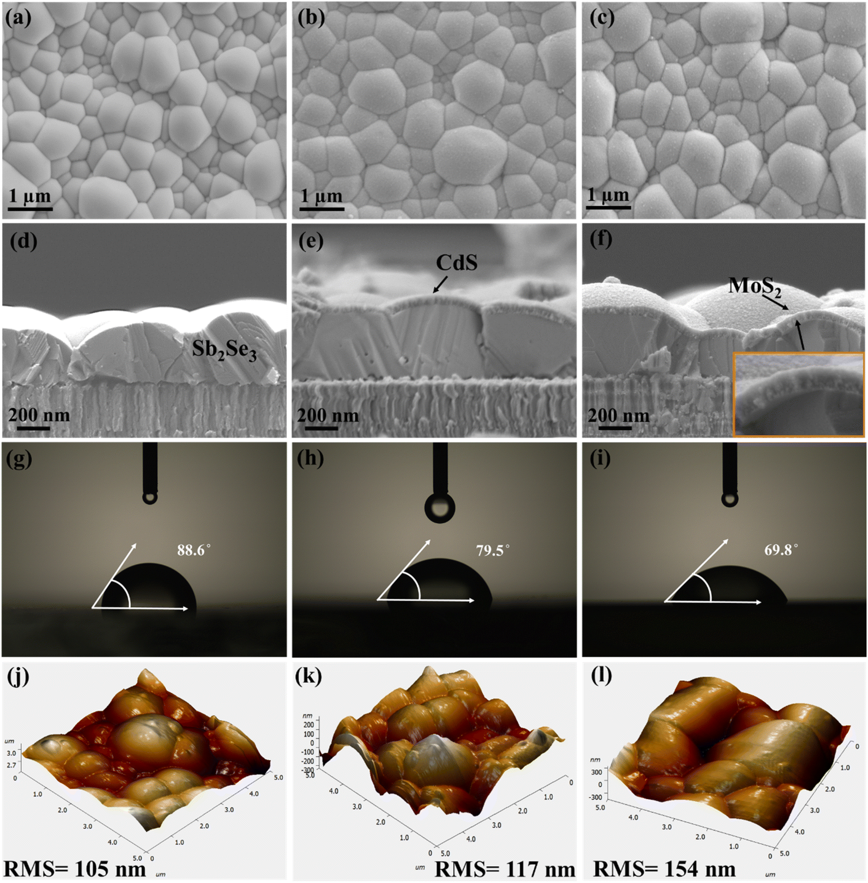 | ||
| Fig. 3 SEM micrographs of (a) Sb2Se3, (b) Sb2Se3/CdS, and (c) Sb2Se3/CdS/MoS2 samples. (d–f) The corresponding cross-sectional SEM images. (g–i) The measured CAs (using H2SO4 electrolyte droplets) of the samples, and (j–l) AFM images of the sample surfaces. | ||
Kelvin probe force microscopy (KPFM) analysis was then performed; this advanced technique allowed us to study the topography and contact potential difference (VCPD) across thin films, providing critical insights into their surface properties. Fig. 4a, e and i show the micrographs, and Fig. 4b, f, and j show the surface potential distributions for Sb2Se3, Sb2Se3/CdS, and Sb2Se3/CdS/MoS2 samples, respectively. The AFM images indicate that the surface morphology of the Sb2Se3 thin films remains consistent across different layer depositions, which correlates well with the top-view SEM micrographs (Fig. 3a–c). The pronounced contrast in CPD between grain interiors and boundaries indicates a strong intergranular carrier extraction, which facilitates efficient charge separation and carrier transport, contributing to enhanced PEC performance. The white arrow line scans, which show CPD variations for Sb2Se3, Sb2Se3/CdS, and Sb2Se3/CdS/MoS2 (M-30), are depicted in Fig. 4c, g, and k, and those for M-20 and M-40 are shown in Fig. S10a and b,† respectively; these scans show the electronic landscape of the samples. The CPD values for Sb2Se3, Sb2Se3/CdS, and Sb2Se3/CdS/MoS2 samples lie in the range of −50 to 30 mV, and a similar decrease in CPD from the grain interior (GI) to the grain boundary (GB) can be observed. This indicates that the sample work function at the GB is lower, i.e., the Fermi energy level EF at the GB is closer to the vacuum level, leading to a downward band bending at the GB. The corresponding schematic diagrams of the energy band structure are presented in Fig. 4d, h and l. Upon further comparison, the average potential difference between the GB and GI for Sb2Se3, Sb2Se3/CdS, and Sb2Se3/CdS/MoS2 are 23, 35, and 45 mV, respectively. Thus, the increased band bending after the deposition of CdS and MoS2 would effectively separate electron–hole pairs by attracting electrons (minority carriers) towards the GBs while promoting holes (majority carriers) to flow into GIs. This mechanism is very important for improving electron extraction and minimizing electron–hole recombination, as well as guiding the charge carriers towards the interface to improve photocurrent generation. Thus, it is predicted to contribute to a higher Jph in photocathode, improving the PEC performance.44
 | ||
| Fig. 4 KPFM scanning surface topography and CPD maps for (a and b) Sb2Se3, (e and f) Sb2Se3/CdS, and (i and j) Sb2Se3/CdS/MoS2 samples, respectively. (c, g and k) The corresponding topography and potential line scans acquired from the white arrow lines. (d, h and l) Schematic of the energy band structure and CPD near the GBs, where “e−” represents electrons; “h+” represents holes. | ||
The photocurrent response and charge transport kinetics of the Sb2Se3-based photocathodes were thoroughly examined. In Fig. 5a, the transient photocurrent decay spectra show that M-20 and M-40 photocathodes exhibited a prominent “spike-like” transient behavior upon light illumination, indicating substantial charge carrier recombination since the temporarily accumulated photoelectrons might easily recombine before reaching a steady state. Conversely, the M-30 photocathode exhibits a very small “spike-like” transient, suggesting reduced charge recombination and improved carrier transport, which is closely related to its optimized surface co-catalyst coverage and photoelectron transport.26 Specifically, the charge transfer efficiency (ηtran) is defined as the ratio of the steady-state photocurrent density (Jss) to the instantaneous photocurrent density (Jinst). The charge separation efficiency (ηsep) can also be obtained using the following equations:26,45
 | (3) |
| Jph = Jabs × ηtran × ηsep | (4) |
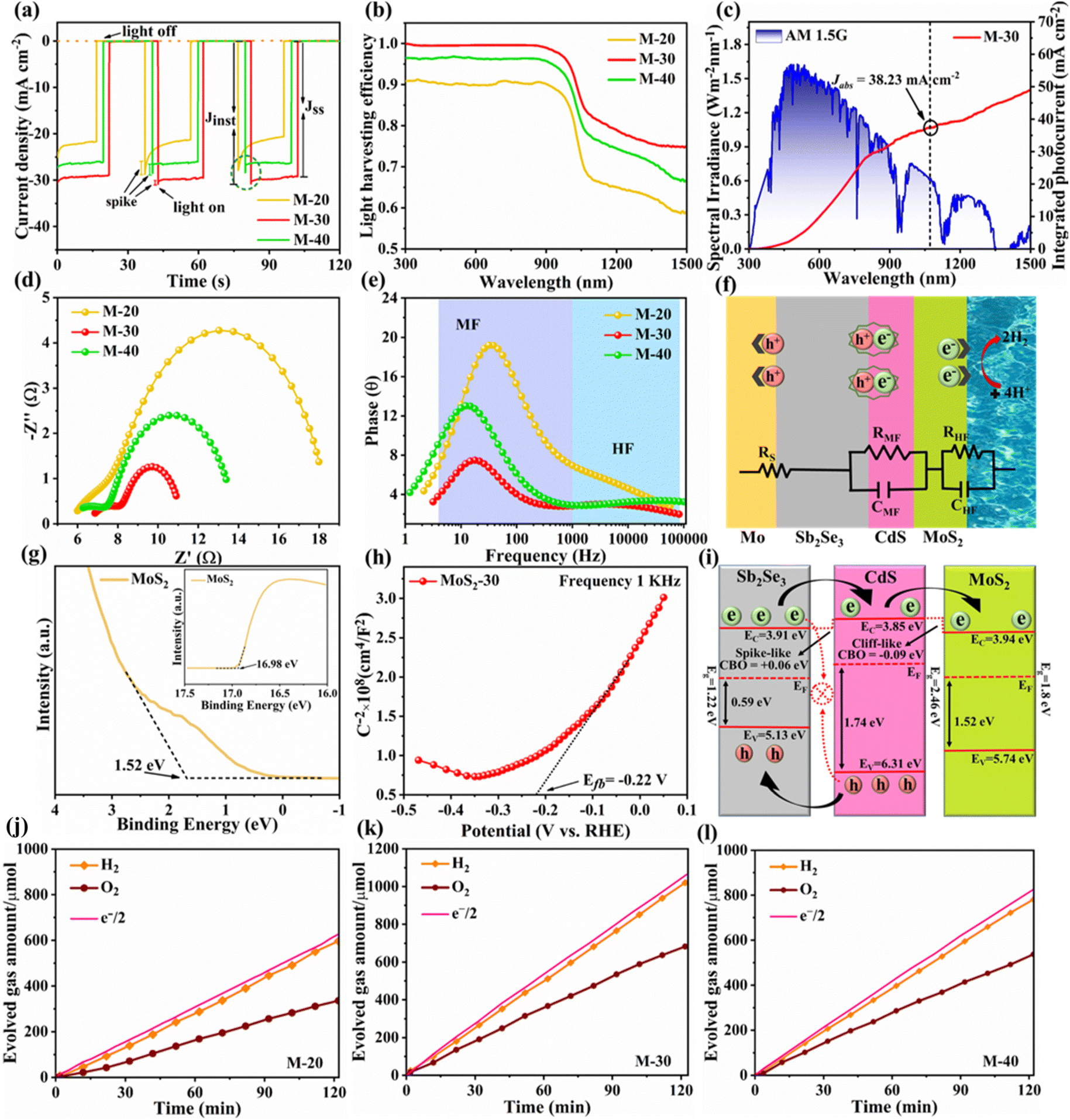 | ||
| Fig. 5 (a) Transient photocurrent response of M-20, M-30, and M-40 photocathodes. (b) Light harvesting efficiency (LHE) of M-20, M-30 and M-40 photocathodes. (c) Energy density flux for the AM 1.5G standard solar spectrum and integrated Jph of the M-30 sample. (d) Nyquist plots and (e) the equivalent Bode plots of M-20, M-30, and M-40 photocathodes. (f) Schematic diagram along with the corresponding equivalent circuit system related to charge carrier dynamics procedures. (g) UPS characterization derived VB positions and SEC edges of the MoS2 thin film. (h) M–S plots of the pure MoS2-30 thin film at a frequency of 1 kHz. (i) Schematic energy band alignment of the Sb2Se3/CdS/MoS2 photocathode. H2 generation amount as a function of AM 1.5G solar light illumination time over the (j) M-20, (k) M-30, and (l) M-40 photocathodes at 0 VRHE for 2 h in pH 1 buffer solution. | ||
As a result, the M-30 photocathode achieved the highest ηtran of 97.31%, as compared to 81.39% and 93.05% for M-20 and M-40, respectively. In parallel, the ηsep for M-30 was also the highest at 82.04%, while M-20 and M-40 exhibited lower values of 51.42% and 69.74%, respectively. The optimized M-30 device simultaneously achieved high charge separation and transport, resulting in improved PEC performance. The theoretical Jph (i.e., Jabs) of the Sb2Se3-based photocathodes was also calculated (Fig. 5b, c, S11a, b and Note S1, ESI†) by using the standard solar spectrum (AM 1.5G) and wavelength-dependent light harvesting efficiency (LHE), and assuming 100% conversion of the absorbed photons to current density. Since λe is ≈1070 nm, the calculations show that the M-30 photocathode achieves a theoretical Jabs of 38.23 mA cm−2 (Fig. 5c), which is the highest among the three samples (Jabs values of 30.04 mA cm−2 and 33.82 mA cm−2 for M-20 and M-40, respectively). The enhanced Jabs for M-30 can be attributed to its ideal MoS2 thickness and light absorption capacity. Photoelectrochemical impedance spectroscopy (PEIS) investigation of Sb2Se3-based photocathodes was conducted to evaluate the charge transfer resistance and specific charge carrier recombination mechanisms within the system. Fig. 5d represents the Nyquist plots for M-20, M-30, and M-40 photocathodes, displaying two distinct arcs for each sample, consistent with the corresponding Bode plots shown in Fig. 5e. The Bode diagram illustrates two different regions, covering the low and high frequencies in the range of 1 to 100 kHz. The PEIS data were fitted using an equivalent circuit model consisting of a series resistance (RS) and two pairs of parallel resistor–capacitor (R–C) elements, as shown in Fig. 5f. The as-fitted results for M-20, M-30, and M-40 photocathodes are presented in Table S1.† In Fig. 5f, RS represents the series resistance at the Mo/Sb2Se3 back contact interface, and the comparable RS values (≈5–6 Ω) across the device indicated a well-established and favorable back interface contact. The high-frequency arc-derived RHF and CHF reflect the charge transfer resistance at the semiconductor heterojunction interface and the associated capacitance within the space charge region. In contrast, RLF and CLF (low frequency arc derivatives) represent the electrochemical charge transfer/reaction resistance within the Helmholtz layer at the electrode–electrolyte interface, along with the corresponding interface/surface-states capacitance.46 Notably, the smaller CHF value (5.03 × 10⁻⁶ F) for the M-30 photocathode implies a shorter charge accumulation time, while the reduced RHF value suggests less interface defects and more effective charge carrier transport and separation efficiencies at the Sb2Se3/CdS heterojunction interface. Furthermore, the minimum RLF value of 4.599 Ω for M-30 as compared to 16.955 Ω for M-20 and 7.929 Ω for M-40 counterparts indicates more efficient HER at the electrode–electrolyte interface under suitable MoS2 co-catalyst loading.
Bulk and interface charge carrier dynamic characteristics strongly affect the PEC performance of the Sb2Se3-based thin films photocathodes. Therefore, ultraviolet photoelectron spectroscopy (UPS) characterization was performed to examine the energy band alignment of the Sb2Se3 absorber, CdS buffer layer (Fig. S11c and d†) and MoS2 (Fig. 5g) thin films to further understand the recombination, transport and separation of charge carriers. According to the secondary electron cut-off (SEC) edge and valence band (VB) position, the conduction band (EC) of MoS2 is −3.94 eV. Compared with the normal hydrogen electrode (NHE), it is −0.50 VNHE, with the conversion implemented by using the following formula:47
| Energy = −eEappl(vs. NHE) − 4.44 eV | (5) |
The conduction band minimum (CBM) of the MoS2 thin film is located above the hydrogen reduction potential, which thermodynamically enhances water reduction with hydrogen evolution through solar water splitting, resulting in an enhanced Jph. Mott–Schottky (M–S) measurements were further performed to investigate the capacitance of MoS2 thin films by examining film capacitance (C) at the semiconductor/electrolyte interface as a function of the applied potential (V). Fig. 5h, S12a and b† demonstrate that 1/C2 increases with potential V in the presence of the space charge region (SCR), demonstrating evident n-type characteristics for MoS2 films.48 Furthermore, the acceptor density (NA) and flat band potential (Efb) were calculated using the following equation:2
 | (6) |
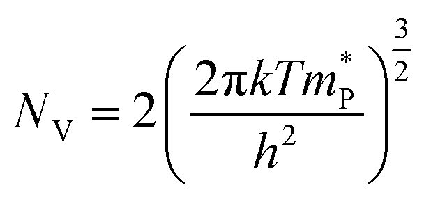
 , and valence band effective density of states function (Nv), by using the following formula:49
 | (7) |
 | (8) |
The MoS2 thin film possesses a similar EV value (−5.74 eV), which matches well with the UPS-derived EV (−5.74 eV). Finally, band bending and energy band alignment for Sb2Se3/CdS/MoS2 are depicted in Fig. 5i. The CdS and MoS2 thin films exhibit stronger n-type conductive characteristics, suggesting that MoS2 would increase the electron carrier density. The valence band offset (VBO) values for n-CdS/p-Sb2Se3 and n-CdS/n-MoS2 are 1.18 eV and 0.57 eV, respectively, which are similar to those reported in previous work (1.14 ± 0.10 eV);50 these values provide the required energy barrier that efficiently stops photo-generated holes from moving toward the electrode–electrolyte interface for recombination. The conduction band alignment between Sb2Se3 and CdS exhibits a “spike-like” band alignment, with a positive conduction band offset (CBO of +0.06 eV), which falls within the optimal range of 0–0.4 eV, suitable for high quality semiconductor heterojunctions. This band alignment decreases energy barriers, enhances charge carrier separation and transport while reducing recombination. After that, the electrons migrate from CdS to the MoS2 layer, which has a slightly higher conduction band edge, further facilitating electron flow. MoS2 acts as a co-catalyst and provides active sites for the HER at the photocathode surface. This layered band structure, with suitable band-bending, confirms efficient electron transport from Sb2Se3 through CdS to MoS2, while holes are directed toward the back contact. Thus, the MoS2 layer improves charge separation and enables effective utilization of photo-generated carriers for hydrogen production, increasing overall PEC efficiency.
Gas chromatography (GC) was used to in situ measure the production of H2 and O2, and then evaluate the photon utilization capability and faradaic efficiency. As shown in Fig. 5j–l, the champion M-30 photocathode demonstrated continuous H2 and O2 evolution at rates of 8.50 and 5.68 μmol min−1, respectively, which are higher than those of M-20 (4.97 and 2.79 μmol min−1) and M-40 (6.51 and 4.47 μmol min−1) photocathodes. Faradaic efficiencies of 91%, 94% and 92% (calculated from the ratio of H2 to e−/2) were obtained for M-20, M-30, and M-40 photocathodes, indicating minimal side reactions or competing redox processes on the photoelectrode surface. After 2 h of continuous irradiation, approximately 1020 μmol of H2 and 682 μmol of O2 were generated by the champion M-30 photocathode, further confirming the durability and versatility of the champion M-30 device for PEC processed solar water splitting. The recorded video in 0.5 M H2SO4 buffer solution under AM 1.5G continuous sunlight irradiation during operation shows continues hydrogen production (Movie S1, ESI†), confirming the excellent PEC performance of the device.
After the successful demonstration of MoS2 as an efficient HER co-catalyst, its secondary role as a protective layer was also examined. The current density–time (J–T) curves for those three devices are shown in Fig. 6a, S13a and b,† under AM 1.5G simulated sunlight illumination at 0 VRHE. As illustrated in Fig. 6a, when the light was switched on, the Jph of M-30 quickly increased from 0 mA cm−2 to 31.03 mA cm−2, and when the light was turned off, it quickly returned to its initial value. This fast and stable response demonstrates the excellent reversibility and stability of the MoS2-based Sb2Se3 photocathodes. In addition to developing a highly efficient photocathode, assessing its real long-term PEC stability is also crucial for practical applications. Fig. 6b displays the photocurrent stability of the champion device (M-30) over 5 h at 0 VRHE under AM 1.5G continuous light irradiation in an H2SO4 buffer solution (pH 1), while Fig. S14a and b† show the stability tests for M-20 and M-40 devices. The thinner MoS2 layer in M-20 likely provides insufficient surface protection due to limited surface coverage to directly expose part of the underlying Sb2Se3/CdS layer to the electrolyte, leading to a higher rate of photo-corrosion and reduced PEC stability. By contrast, the champion M-30 photocathode demonstrated remarkable stability over the 5 h testing period, retaining approximately 90% of its initial Jph under continuous light irradiation. The LSV curves and PEC performance before and after the stability test are shown in Fig. S14c, d and Movie S2.† Its excellent stability is closely related to the MoS2 layer with appropriate thickness, which effectively protects the Sb2Se3/CdS surface, avoiding localized dissolution that could induce thermodynamic photo-corrosion and degradation during prolonged operation. This finding is consistent with other studies in which Sb2Se3 photocathodes were protected by additional layers like C60 or TiO2 to prevent CdS degradation.26 Table S2† presents a comparative analysis of the PEC performance and stability of Sb2Se3-based photocathodes using MoS2 and Pt as co-catalysts. This comparison highlights the effectiveness of MoS2 as a low-cost alternative to noble metal catalysts while maintaining competitive PEC activity and durability. To further evaluate the intrinsic stability and lifespan of the Sb2Se3 absorber (Fig. S13c†), bare MoS2 film (Fig. S13d†), and M-30 thin-film photocathode (Fig. 6c), a photo-corrosion stress test was conducted using cyclic voltammetry. No significant photo-corrosion currents or redox peaks were observed in any of the samples after 100 cycles, strongly suggesting their exceptional tolerance to photo-corrosion during practical PEC applications. As shown in Fig. 6d–g, the PEC performance and stability of the champion M-30 photocathode also varies significantly across different pH buffer solutions. Specifically, it exhibited a Jph of 31.01, 19.67, and 9.60 mA cm−2, and HC-STH efficiencies of 3.06%, 1.67%, and 0.75% in pH 1, pH 3, and pH 6.5 buffer solutions, respectively, confirming the faster and more efficient HER in acidic buffer solution. Moreover, its photocurrent stability (3 h duration) under acidic conditions (pH 1) is superior to that in neutral (pH 6.5) electrolytes. It is similar to some previous reports, e.g., MoSx co-catalyst modified CZTS and InP photocathodes, both of which exhibit high photocurrent and good stability in acidic conditions as compared to neutral buffer solution.29,35 As shown in Fig. 6h, this behavior can be described by the fact that, in acidic environments with a higher concentration of H+ ions, photo-excited electrons can more easily and efficiently combine ionically to produce hydrogen gas.51 The rapid transport of photo-excited electrons in an acidic buffer solution could also mitigate the photo-corrosion of the photoelectrode, and hence increase the PEC stability of the photocathode.3 These findings are particularly important for optimizing photocathode design for practical solar-driven hydrogen production applications. The enhanced PEC performance under acidic conditions expands the potential applications of these photocathodes to electrocatalysis, sensors, and environmental remediation, where stability under harsh conditions is often a critical requirement.
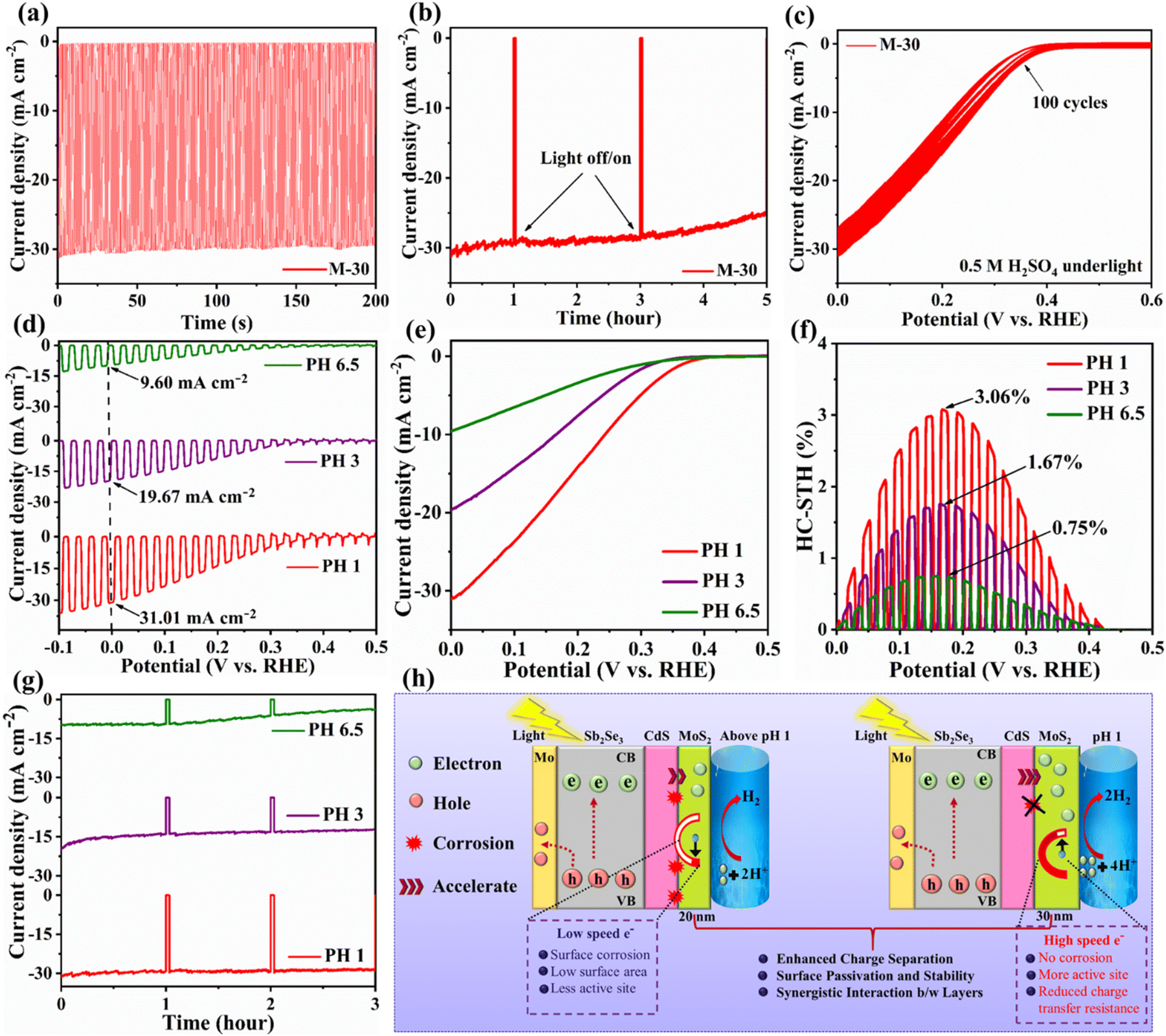 | ||
| Fig. 6 (a) J–T curve of the M-30 photocathode at 0 VRHE under AM 1.5G simulated solar irradiation. (b) Photocurrent stability experiment of the champion M-30 photocathode at 0 VRHE under continuous sunlight illumination within 5 hours. (c) CV measurement of the M-30 photocathode in 0.5 M H2SO4 under illumination. J–V curves of the M-30 photocathode at different pH solution, and (d) under chopped light, and (e) under continuous light irradiation. (f) The calculated HC-STH conversion efficiencies. (g) Stability of M-30 photocathodes in pH 1, pH 3, and pH 6.5 solution under AM 1.5G simulated light irradiation. (h) Mechanism schematic representation of the PEC performance Mo/Sb2Se3/CdS/MoS2 photocathodes. | ||
4. Conclusion
In this work, we successfully demonstrated the enhancement of Sb2Se3-based photocathodes for solar hydrogen generation by the introduction of MoS2 as a cost-effective, noble-metal-free co-catalyst. The optimized Sb2Se3/CdS/MoS2 photocathode achieved a record Jph of 31.03 mA cm−2 at 0 VRHE and a HC-STH efficiency of 3.08% in a pH 1 buffer solution. The MoS2 co-catalyst played an important role in increasing the overall performance by decreasing photo-corrosion, electron–hole recombination, and charge transfer resistance at the semiconductor/electrolyte interface. Our systematic investigation shows that MoS2 not only facilitated efficient charge carrier transport but also improved light-harvesting efficiency by optimizing the band alignment at the Sb2Se3/CdS interface. This dual function of MoS2, as a co-catalyst and a protective layer, contributed to a stable, high-performance photocathode capable of sustained hydrogen evolution over extended periods under acidic conditions. Additionally, the photocathode exhibited improved stability and performance across a range of pH conditions, making it a promising candidate for practical applications in solar hydrogen production. In short, the combination of Sb2Se3 and MoS2 offers a feasible, eco-friendly alternative to Pt-based devices, advancing the development of efficient and cost-effective photocathodes for hydrogen production.Data availability
The data supporting this article have been included as part of the ESI.†Author contributions
Munir Ahmad: data curation, investigation, methodology, conceptualization, writing – original draft. Anadil Gul: methodology, investigation. Hafiz Sartaj Aziz: methodology, investigation. Tahir Imran: data curation, formal analysis. Muhammad Ishaq: data curation, investigation. Muhammad Abbas: data curation, investigation. Zhenghua Su: methodology, investigation. Shuo Chen: conceptualization, formal analysis, writing – review & editing, supervision, funding acquisition.Conflicts of interest
The authors declare no conflict of interest.Acknowledgements
This work was supported by the National Natural Science Foundation of China (No. 62474114), Guangdong Basic and Applied Basic Research Foundation (2023A1515011256), China, Science and Technology plan project of Shenzhen (JCYJ20240813141620027), China. The authors are grateful to Prof. Yu-Jia Zeng for assistance with KPFM characterization, at Shenzhen University.References
- Y. Xia, M. Zhu, L. Qin, C. Zhao, D. Hong, Y. Tian, W. Yan and Z. Jin, Energy Mater., 2023, 3, 300004 CrossRef CAS.
- G. Liang, Z. Li, M. Ishaq, Z. Zheng, Z. Su, H. Ma, X. Zhang, P. Fan and S. Chen, Adv. Energy Mater., 2023, 13, 2300215 CrossRef CAS.
- J. Tan, W. Yang, Y. Oh, H. Lee, J. Park, R. Boppella, J. Kim and J. Moon, Adv. Energy Mater., 2019, 9, 1900179 CrossRef.
- T. Zhou, S. Chen, J. Wang, Y. Zhang, J. Li, J. Bai and B. Zhou, Chem. Eng. J., 2021, 403, 126350 CrossRef CAS.
- C. M. Jiang, S. E. Reyes-Lillo, Y. Liang, Y.-S. Liu, G. Liu, F. M. Toma, D. Prendergast, I. D. Sharp and J. K. Cooper, Chem. Mater., 2019, 31, 2524–2534 CrossRef CAS.
- C. Li, T. Hisatomi, O. Watanabe, M. Nakabayashi, N. Shibata, K. Domen and J. J. Delaunay, Appl. Phys. Lett., 2016, 109, 033902 CrossRef.
- J. Zhao, T. Minegishi, H. Kaneko, G. Ma, M. Zhong, M. Nakabayashi, T. Hisatomi, M. Katayama, N. Shibata and T. Yamada, Chem. Commun., 2019, 55, 470–473 RSC.
- A. D. DeAngelis, K. Horsley and N. Gaillard, J. Phys. Chem. C, 2018, 122, 14304–14312 CrossRef CAS.
- M. Chen, Y. Liu, C. Li, A. Li, X. Chang, W. Liu, Y. Sun, T. Wang and J. Gong, Energy Environ. Sci., 2018, 11, 2025–2034 RSC.
- B. Koo, D. Kim, P. Boonmongkolras, S. R. Pae, S. Byun, J. Kim, J. H. Lee, D. H. Kim, S. Kim and B. T. Ahn, ACS Appl. Energy Mater., 2020, 3, 2296–2303 CrossRef CAS.
- J. Song, B. Teymur, Y. Zhou, E. Ngaboyamahina and D. B. Mitzi, ACS Appl. Energy Mater., 2021, 4, 81–87 CrossRef CAS.
- J. Tan, B. Kang, K. Kim, D. Kang, H. Lee, S. Ma, G. Jang, H. Lee and J. Moon, Nat. Energy, 2022, 7, 537–547 CrossRef CAS.
- J. Tan, W. Yang, H. Lee, J. Park, K. Kim, O. S. Hutter, L. J. Phillips, S. Shim, J. Yun and Y. Park, Appl. Catal., B, 2021, 286, 119890 CrossRef CAS.
- W. Yang, J. H. Kim, O. S. Hutter, L. J. Phillips, J. Tan, J. Park, H. Lee, J. D. Major, J. S. Lee and J. Moon, Nat. Commun., 2020, 11, 861 CrossRef CAS.
- S. Zhang, M. Long, P. Zhang, J. Wang, H. Lu, H. Xie, A. Tang and H. Yang, Chem. Eng. J., 2022, 429, 132091 CrossRef CAS.
- L. Zhang, Y. Li, C. Li, Q. Chen, Z. Zhen, X. Jiang, M. Zhong, F. Zhang and H. Zhu, ACS Nano, 2017, 11, 12753–12763 CrossRef CAS.
- W. Yang, J. Park, H. C. Kwon, O. S. Hutter, L. J. Phillips, J. Tan, H. Lee, J. Lee, S. D. Tilley, J. D. Major and J. Moon, Energy Environ. Sci., 2020, 13, 4362–4370 RSC.
- P. C. Vesborg, B. Seger and I. Chorkendorff, J. Phys. Chem. Lett., 2015, 6, 951–957 CrossRef CAS PubMed.
- Y. Li, S. Wang, J. Chen, O. Lin, Z. Yin, C. Yang and A. Tang, J. Semicond., 2023, 44, 122701 CrossRef CAS.
- L. Guo, P. S. Shinde, Y. Ma, L. Li, S. Pan and F. Yan, Sol. RRL, 2020, 4, 1900442 CrossRef CAS.
- X. Chen, J. Zhao, G. Li, D. Zhang and H. Li, Energy Mater., 2022, 2, 200001 CAS.
- M. Medina, P. G. Corradini and L. H. Mascaro, J. Braz. Chem. Soc., 2019, 30, 2210–2218 CAS.
- P. Shinde, P. Fontenot, J. Donahue, J. Waters, P. Kung, L. McNamara, N. Hammer, A. Gupta and S. Pan, J. Mater. Chem. A, 2018, 6, 9569–9582 RSC.
- C. G. Morales-Guio, S. D. Tilley, H. Vrubel, M. Grätzel and X. Hu, Nat. Commun., 2014, 5, 3059 CrossRef PubMed.
- J.-H. Huang, H. H. Chen, P. S. Liu, L.-S. Lu, C. T. Wu, C. T. Chou, Y. J. Lee, L. J. Li, W. H. Chang and T. H. Hou, Mater. Res. Express, 2016, 3, 065007 CrossRef.
- G. Liang, T. Liu, M. Ishaq, Z. Chen, R. Tang, Z. Zheng, Z. Su, P. Fan, X. Zhang and S. Chen, Chem. Eng. J., 2022, 431, 133359 CrossRef CAS.
- K. Feng, D. Huang, L. Li, K. Wang, J. Li, T. Harada, S. Ikeda and F. Jiang, Appl. Catal., B, 2020, 268, 118438 CrossRef CAS.
- C. Liu, T. Liu, Y. Li, Z. Zhao, D. Zhou, W. Li, Y. Zhao, H. Yang, L. Sun and F. Li, J. Mater. Chem. A, 2020, 8, 23385–23394 RSC.
- R. R. Prabhakar, W. Septina, S. Siol, T. Moehl, R. Wick-Joliat and S. D. Tilley, J. Mater. Chem. A, 2017, 5, 23139–23145 RSC.
- J. Tan, W. Yang, Y. Oh, H. Lee, J. Park and J. Moon, ACS Appl. Mater. Interfaces, 2018, 10, 10898–10908 CrossRef CAS PubMed.
- Q. Ding, F. Meng, C. R. English, M. Cabán-Acevedo, M. J. Shearer, D. Liang, A. S. Daniel, R. J. Hamers and S. Jin, J. Am. Chem. Soc., 2014, 136, 8504–8507 CrossRef CAS PubMed.
- A. Standing, S. Assali, L. Gao, M. A. Verheijen, D. Van Dam, Y. Cui, P. H. Notten, J. E. Haverkort and E. P. Bakkers, Nat. Commun., 2015, 6, 7824 CrossRef CAS.
- T. C. Dang, T. Dai Nguyen, T. H. Truong, M. T. Man, T. T. H. Bui, T. K. C. Tran, P. D. Truong, C. K. Nguyen, V. C. Nguyen and D. B. Seo, Mater. Sci. Semicond. Process., 2021, 121, 105308 CrossRef CAS.
- A. Alarawi, V. Ramalingam, H. C. Fu, P. Varadhan, R. Yang and J. H. He, Opt. Express, 2019, 27, A352–A363 CrossRef CAS PubMed.
- L. Gao, Y. Cui, J. Wang, A. Cavalli, A. Standing, T. T. Vu, M. A. Verheijen, J. E. Haverkort, E. P. Bakkers and P. H. Notten, Nano Lett., 2014, 14, 3715–3719 CrossRef CAS.
- W. Gu, F. Yang, C. Wu, Y. Zhang, M. Shi and X. Ma, Nanoscale Res. Lett., 2014, 9, 1–6 CrossRef CAS PubMed.
- G. J. Chen, R. Tang, S. Chen, Z. H. Zheng, Z. H. Su, H. L. Ma, X. H. Zhang, P. Fan and G.-X. Liang, ACS Appl. Mater. Interfaces, 2022, 14, 31986–31997 CrossRef CAS PubMed.
- N. B. Shinde and S. K. Eswaran, J. Phys. Chem. Lett., 2021, 12, 6197–6202 CrossRef CAS PubMed.
- Z. Wei, W. Mao, J. Liu, Y. Xiao, M. Zhu and Y. Tian, J. Mater. Sci.: Mater. Electron., 2020, 31, 4574–4581 CrossRef CAS.
- J. Chastain and R. C. King Jr, Handbook of X-ray photoelectron spectroscopy, Perkin-Elmer Corporation, 1992, vol. 40, p. 221 Search PubMed.
- M. B. Costa, F. W. Lucas, M. Medina and L. H. Mascaro, ACS Appl. Energy Mater., 2020, 3, 9799–9808 CrossRef CAS.
- Y. T. Ho, C. H. Ma, T. T. Luong, L. L. Wei, T. C. Yen, W. T. Hsu, W. H. Chang, Y. C. Chu, Y. Y. Tu and K. P. Pande, Phys. Status Solidi RRL, 2015, 9, 187–191 CrossRef CAS.
- F. Foadi, G. H. ten Brink, M. R. Mohammadizadeh and G. Palasantzas, J. Appl. Phys., 2019, 125, 244307 CrossRef.
- P. Luo, T. Imran, D. L. Ren, J. Zhao, K. W. Wu, Y. J. Zeng, Z. H. Su, P. Fan, X. H. Zhang and G. X. Liang, Small, 2024, 20, 2306516 CrossRef CAS PubMed.
- J. H. Kim and J. S. Lee, Adv. Mater., 2019, 31, 1806938 CrossRef.
- W. Yang, T. Moehl, E. Service and S. D. Tilley, Adv. Energy Mater., 2021, 11, 2003569 CrossRef CAS.
- R. Beranek, Adv. Phys. Chem., 2011, 2011, 786759 CrossRef.
- K. Sun, C. Yan, F. Liu, J. Huang, F. Zhou, J. A. Stride, M. Green and X. Hao, Adv. Energy Mater., 2016, 6, 1600046 CrossRef.
- M. D. Bhatt and J. S. Lee, J. Mater. Chem. A, 2015, 3, 10632–10659 RSC.
- C. Yan, F. Liu, N. Song, B. K. Ng, J. A. Stride, A. Tadich and X. Hao, Appl. Phys. Lett., 2014, 104, 173901 CrossRef.
- Q. Ding, B. Song, P. Xu and S. Jin, Chem, 2016, 1, 699–726 CAS.
Footnote |
| † Electronic supplementary information (ESI) available. See DOI: https://doi.org/10.1039/d5sc01663k |
| This journal is © The Royal Society of Chemistry 2025 |