
 Open Access Article
 This Open Access Article is licensed under a Creative Commons Attribution-Non Commercial 3.0 Unported Licence
A Zn-doped Sb2Te3 flexible thin film with decoupled Seebeck coefficient and electrical conductivity via band engineering†
Zi-long
Zhang
,
Wen-yu
Yang
,
Bo
Wu
,
Mohammad
Nisar
,
Fu
Li
 ,
Guang-xing
Liang
,
Jing-ting
Luo
,
Yue-xing
Chen
and
Zhuang-hao
Zheng
*
,
Guang-xing
Liang
,
Jing-ting
Luo
,
Yue-xing
Chen
and
Zhuang-hao
Zheng
*
Shenzhen Key Laboratory of Advanced Thin Films and Applications, Key Laboratory of Optoelectronic Devices and Systems of Ministry of Education and Guangdong Province, State Key Laboratory of Radio Frequency Heterogeneous Integration, College of Physics and Optoelectronic Engineering, Shenzhen University, Shenzhen, Guangdong 518060, China. E-mail: zhengzh@szu.edu.cn
First published on 22nd January 2025
Abstract
Sb2Te3-based flexible thin films can be utilized in the fabrication of self-powered wearable devices due to their huge potential in thermoelectric performance. Although doping can significantly enhance the power factor value, the process of identifying suitable dopants is typically accompanied by numerous repeating experiments. Herein, we introduce Zn doping into thermally diffused p-type Sb2Te3 flexible thin films with a candidate dopant validated using the first-principles calculations. Subsequent experiments further corroborated the successful introduction of a Zn dopant and the improvement of thermoelectric performance. Specifically, p-type doping and the increase in the calculated effective mass can significantly increase the Seebeck coefficient, achieving the decoupling of the Seebeck coefficient and electrical conductivity in Sb2Te3 flexible thin films. An outstanding power factor of ∼22.93 μW cm−1 K−2 at room temperature can be obtained in the 0.58% Zn doped Sb2Te3 sample with significant flexibility. The subsequent fabrication of a flexible thermoelectric generator provides the maximum output voltage and output power of ∼53.0 mV and ∼1100 nW with a temperature difference of 40 K, respectively, pointing out the huge potential of Zn-doped Sb2Te3 materials for thermoelectric applications in self-powered wearable devices.
1. Introduction
To meet the increasing requirement of self-powered wearable devices, flexible thermoelectric generators (F-TEGs) have been investigated deeply because of their unique capability that can convert heat energy to electricity based on the temperature difference.1–3 Suitable F-TEGs for wearable devices should possess high thermoelectric (TE) performance and flexibility. Generally, the TE performance of a material can be evaluated by using a dimensionless figure of merit, ZT = S2σT∕κ, where S, σ, T and κ are the Seebeck coefficient, electrical conductivity, absolute temperature and total thermal conductivity, respectively.4–7 To achieve a higher TE performance, a higher power factor (PF = S2σ) and lower κ should be considered with a relevant carrier concentration (n).8,9 However, the increase in n leads to an increase in σ and a decrease in S. Thus, the decoupling of S and σ is one of the most attractive topics in the research field of TE materials. Generally, since κ is hard to measure in thin films, the improvement of PF is more vital in improving TE performance. Recently, flexible thin films were gradually attracting researchers' attention, since they exhibit high TE properties and flexibility simultaneously.10Antimony telluride (Sb2Te3) is one of the most investigated TE materials near room temperature in the recent decades, possessing a narrow band gap (Eg ∼ 0.161 eV) without toxicity.11–14 Typically, TE materials with a narrow band gap provide huge potential for TE improvement, especially the Seebeck coefficient and electrical conductivity.15,16 In recent years, multiple methods were used to improve the TE performance of bulk Sb2Te3, especially doping methods.17,18 Kim et al.19 introduced dense dislocation arrays at the grain boundaries of Bi0.5Sb1.5Te3 through liquid-phase Te extrusion, achieving an increase in the ZT value of 1.86 ± 0.15 at 320 K. This significant ZT value provides sufficient material performance (ZT > 1) for the application of TEGs. However, the TE performance of thin films is typically lower than that of bulk materials. Currently, there are multiple types of methods to enhance the TE performance of thin films, such as the synthesis method,20,21 doping,22,23 ferroelectric polarization,24 and annealing.25,26 Tan et al.27 combined thermal evaporation deposition, post-annealing treatment and the Bi doping method together, obtaining a Bi0.5Sb1.5Te3 thin film with an ultrahigh ZT value of ∼1.5 and PF of ∼36 μW cm−1 K−2 near room temperature. According to our previous studies, Bi-doped Sb2Te3 thin films can achieve a ZTmax of ∼1.11 at 393 K and PF of ∼21 μW cm−1 K−2 near room temperature, using a novel fabrication process of the directed thermal diffusion method.28 This significant improvement of TE performance and the directed thermal diffusion method demonstrate the success of the control of n via the doping method, and the maturity of the fabrication procedure.
Since pristine Sb2Te3 shows p-type semiconductor behavior, the carrier (hole) concentration should be improved by p-type doping. Thus, a candidate element with a 1+ or 2+ cation valence state should be introduced into Sb2Te3 for Sb vacancies (VSb). Thus, the first-principles calculation of the band structure using density functional theory (DFT) was conducted to simulate the band structure development after p-type doping. To consider the candidate dopants scientifically, we would like to first narrow down the potential dopants to cations only, and further verify their feasibility before fabrication via DFT calculations, which saves time and cost for experiments on dopant selection. In this work, we first evaluated the change in the Fermi level in Zn-doped p-type Sb2Te3, with a significant decreasing at the top of the valence band, which illustrates the successful introduction of p-type doping. We then prepared Zn-doped p-type Sb2Te3 thin films using the same fabrication procedure according to our previous work, which is the directional thermal diffusion method. The schematic diagrams of the fabrication procedure are shown in Fig. 1(d)–(f). The crystal structure, valence state, and lattice morphology characterization results showed the successful introduction of Zn, and Zn replaces the Sb sites. The σ, S and PF values are enhanced after Zn-doping due to the improvement of n, which also supports that p-type doping occurred in p-type Sb2Te3 thin films via DFT calculations. The increased calculated effective mass also provides evidence that S can be improved by Zn-doping, achieving the decoupling of S and σ. An outstanding PF value of 22.93 μW cm−1 K−2 near room temperature can be achieved in the Zn 0.58% sample with significant mechanical flexibility. The subsequent f-TEG with Zn 0.58% sample as the p-leg provides the maximum output voltage and output power of ∼53.0 mV and ∼1100 nW at a temperature difference of 40 K. Compared to our previous work which outstandingly achieved a PF of ∼21 μW cm−1 K−2 at room temperature, this work provides significant reduction in time and cost but higher TE performance via the evaluation of computational calculations.
 | ||
| Fig. 1 (a) Comparison of PF values with those in the references; calculated band structures of the (b) pristine and (c) Zn-doped Sb2Te3 material by DFT calculations; (d) schematic diagram of the fabrication process of a Sb/Zn precursor thin film by magnetron sputtering; (e) schematic diagram of the fabrication process of a Te precursor thin film by thermal evaporation; (f) schematic diagram of the thermal diffusion process using Sb/Zn and Te precursor thin films. | ||
2. Experimental details
2.1 Thin film fabrication
Zn-Doped Sb2Te3 thin films were prepared on polyimide (PI) substrates by the thermal diffusion method using a Sb/Zn precursor thin film and Te precursor thin film. At first, the PI substrate was cut into 20 mm × 20 mm × 0.12 mm, and then ultrasonically cleaned by using deionized water, ethanol and finally acetone one by one for 20 minutes. Second, the Sb/Zn precursor thin film was deposited on a PI substrate using the magnetron sputtering technique. As Fig. 1(d) shows, both the Sb target material (99.99% purity) and Zn target material (99.99% purity) were placed in a vacuum chamber. The vacuum degree of the chamber was set as 3.0 × 10⁻³ Pa. The working pressure of Sb/Zn precursor thin film fabrication is 0.5 Pa with an argon (Ar) flow of 40 sccm. The Zn target was deposited on a PI substrate by direct current magnetron sputtering with a current power of 15 W. The change in deposition time on the Zn target resulted in different Zn doping contents. In contrast, the Sb target was deposited on a PI substrate by radio frequency magnetron sputtering with a current power of 60 W. The deposition time of the Sb target was around 7 minutes. For the synthesis of Te precursor thin films, Te powders (99.99% purity) were placed in a vacuum deposition chamber of a tantalum reaction boat on a PI substrate, as shown in Fig. 1(e). The vacuum degree of the deposition chamber was set as 4.5 × E−5 mTorr. The current power of the evaporation was 20 W, increasing at a rate of 2 W min−1. The deposition time was around 12 minutes, and the thickness of the Te precursor thin film was around 480 nm. Finally, the Sb/Zn and Te precursor thin films were in close contact in a mold, and then heat treatment was performed in a vacuum at 360 °C for 30 minutes, as shown in Fig. 1(f). The Te precursor thin film part was closer to the heat source under the mold. Thus, Zn/Sb and Te precursor thin films were diffused in the mold under heat and pressure, and formed a Sb2Te3 thin film with Zn doping. In contrast to the traditional co-sputtering or co-evaporation methods, which control thin film compositions through annealing or in situ heating, the thermal diffusion process can precisely control the composition of thin films by adjusting the thickness of precursor layers.2.2 Characterization
X-ray diffraction (XRD, D/max-2500, Rigaku Corporation) was used to characterize the crystal structure of the synthesized samples with the scanning range of 2θ = 10° to 80°. The distribution and analysis of the valence states of elements was conducted by using an X-ray photoelectron spectroscope (XPS; ESCALAB Xi+, Thermo Fisher, USA). The surface and cross-sectional morphology of the synthesized samples were observed by field-emission scanning electron microscopy (SEM, Supra 55 Sapphire, Zeiss) and the elemental composition was analyzed by using the equipped energy dispersive X-ray spectrometer (EDS, BRUKER QUANTAX 200, Zeiss). The high-resolution nanostructure development of the synthesized samples was observed and analyzed by using a spherical aberration-corrected transmission electron microscope (AC-TEM, FEI, Titan3 Themis G2). The S and σ of the synthesized samples were measured by using SBA apparatus (SBA458, Netzsch). The carrier concentration (n) and carrier mobility (μ) at room temperature were measured by using a Hall measurement system (HL5500PC, Nanometrics). The thickness of the synthesized thin films was measured by using a surface-profile measurement system (Bruker Dektak XT). A home-made automatic bending device was used to investigate the mechanical flexibility and durability of the synthesized thin films with different bending radii. The band structure information of pristine and Zn-doped Sb2Te3 was calculated by the projector augmented wave method as implemented in the VASP code.29 The exchange–correlation functional was approximated using the generalized gradient approximation with Perdew–Burke–Ernzerhof parametrization.30,31 Detailed calculation procedures were illustrated in our previous work.283. Results and discussion
Essentially, because p-type doping leads to an increase in hole concentration which further enhances σ in Sb2Te3 materials, the development of the band structure should be calculated and analyzed by the first principles of DFT. Fig. 1(b) and (c) show the band structure of the pristine and Zn-doped Sb2Te3 material, respectively. Pristine Sb2Te3 possesses a relatively low bandgap of 0.118 eV, which leads to a relatively high S. In addition, the Fermi level of Zn-doped Sb2Te3 shifts to the top pf the valence band compared to that of pristine Sb2Te3. Thus, Zn can be considered as a dopant that can introduce p-type doping to increase the hole concentration in p-type Sb2Te3, and further enhance the σ.Table S1† shows the Sb, Te, and Zn compositions of the synthesized Zn-doped Sb2Te3 thin films. The pristine Sb2Te3 thin film was prepared by using a Sb precursor film. The synthesized Zn-doped samples were named according to the content of Zn, which are 0.21%, 0.58%, 0.73%, and 1.18%, respectively. Fig. 2(a) shows the XRD patterns of Zn doped samples and the pristine sample compared to the standard PDF card (PDF# 15-0874) of Sb2Te3 from 2θ = 10° to 80°. All the synthesized thin film samples possess the same characteristic peaks compared to the standard PDF card. No secondary phases are formed according to the patterns. The main diffraction peaks of all the samples are located at the (015), (1010), (110), and (205) planes. Since the (015) plane has the strongest intensity in the patterns, it can be proved that the synthesized thin film samples exhibit preferential growth along the (015) plane. A careful examination of the (015) diffraction peak in the XRD patterns (Fig. 2(b)) demonstrates that, with increasing Zn content, the (015) diffraction peak shifts to higher angles, indicating a reduction in the lattice volume. To better illustrate the changes in lattice volume, the lattice parameters a and c with varying Zn contents are recorded in Fig. 2(c). Both a and c show a decreasing tendency with the increase in Zn content, pointing out the incorporation of Zn doping into the lattice of Sb2Te3.
 | ||
| Fig. 2 (a) XRD patterns of the synthesized Zn-doped thin film samples with pristine Sb2Te3 from 10° to 80°; (b) the enlarged XRD patterns of the (015) diffraction peak; (c) the development of lattice parameters a and c with increasing Zn content; XPS spectra of Zn-doped Sb2Te3 samples and Gaussian-fitted valence states in XPS spectra: (d) Sb 3d, (e) Te 3d, and (f) Zn 2p. | ||
In addition to XRD, the valence states of the elements in the Zn-doped Sb2Te3 thin film samples were studied by XPS. Fig. 2(d)–(f) show the XPS spectra of Sb, Te, and Zn from the Zn-doped Sb2Te3 samples, respectively. Fig. 2(d) shows that the binding energy of Sb 3d3/2 and Sb 3d5/2 is located at ∼539.88 eV and ∼530.53 eV, which are higher than the standard values of ∼537.6 eV and ∼528.2 eV, respectively. According to the increase in binding energy, Zn doping can effectively introduce p-type doping, lower the Fermi level and induce lattice distortion, which also verifies the hypothesis before the experiments. Fig. 2(e) shows that the binding energy of Te 3d3/2 and Te 3d5/2 is located at ∼583.18 eV and 572.83 eV, which are similar to the standard values of ∼583.3 eV and 572.9 eV. Thus, Sb 3d and Te 3d show the valence states of +3 and −2 in Sb2Te3 materials, respectively. Fig. 2(f) demonstrates that the binding energy of Zn 2p1/2 and Zn 2p3/2 is located at ∼1041.58 eV and 1023.13 eV, which is different from the standard values of ∼1044.8 and ∼1021.8 eV, respectively. After Zn doping, the 3 holes from Sb are substituted by the 2 holes provided by Zn, resulting in p-type doping in Sb2Te3 materials. Combining with the absence of secondary phases in the samples from XRD results, Zn only replaces Sb in Sb2Te3 materials, causing p-type doping and lowering the Fermi level.
To better observe the microstructural development of the Zn-doped thin films, Fig. 3(a)–(d) show the surface morphology of Zn 0.21%, Zn 0.73%, Zn 1.18%, and Zn 0.58% Sb2Te3 thin film samples under SEM, respectively. All the observed areas show a dense Sb2Te3 phase with relatively large grains. Fig. S1(a)–(d)† show the cross-sectional area morphology of Zn 0.21%, Zn 0.58%, Zn 0.73%, and Zn 1.18% thin film samples under SEM. As the figures show, the high crystallinity and highly ordered growth in the vertical direction of the thin film can be observed. The thickness of the synthesized thin film samples is from 550 nm to 610 nm. Fig. 3(e) shows the mapping of the Zn 0.58% sample under EDS scanning with the elemental distribution of Zn-doped Sb2Te3 thin films. As the figure shows, all the elements are distributed uniformly in the observed area of the thin film without any aggregation. The EDS elemental distribution mapping and scanning of the Zn 0.58% sample are shown in Fig. 3(f), showing that all the elements detected are uniformly distributed in the vertical direction of the thin film without any aggregation. Moreover, no obvious secondary phases are formed in all the observed morphologies. Therefore, the SEM images and EDS elemental distributions both indicate the success of the synthesis route of the directional thermal diffusion method, using the precursor thin films prepared by the magnetron sputtering and thermal evaporation methods, with an acceptable thickness of thin film samples.
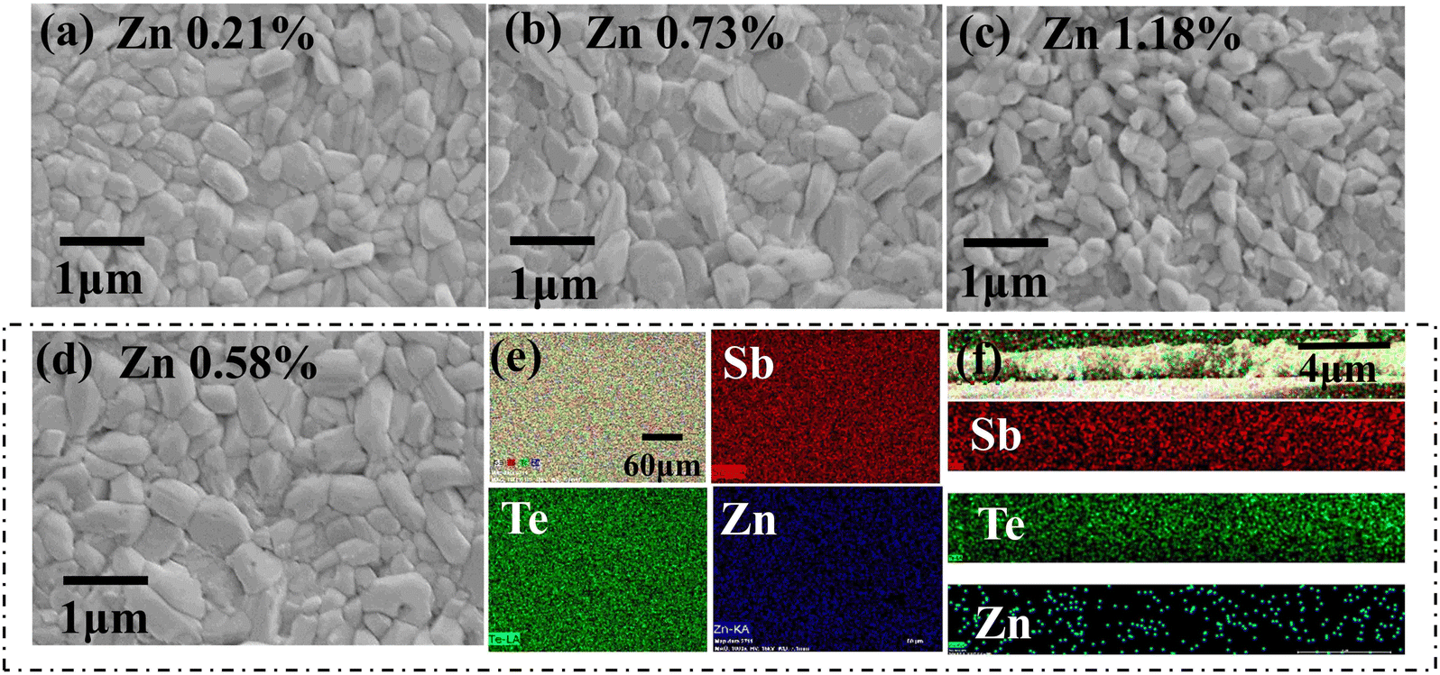 | ||
| Fig. 3 SEM images of the surface morphology in (a) Zn 0.21%, (b) Zn 0.73%, (c) Zn 1.18%, and (d) Zn 0.58% Sb2Te3 thin film samples; (e) EDS mapping image of the Zn 0.58% sample surface with Sb, Te, and Zn and the distribution of all three elements; (f) EDS mapping image of Zn 0.58% sample cross-sectional area with Sb, Te, and Zn and the distribution of all three elements. | ||
To investigate the effect of Zn doping on the nanostructure of Sb2Te3 materials, TEM characterization was conducted. Fig. 4(a) shows a low-resolution TEM image of the Zn 0.58% sample with a well crystallized structure. Fig. 4(b) shows the high resolution high-angle annular dark field (HR-HAADF) image of the blue circled area in Fig. 4(a). As the figures show, the synthesized Zn 0.58% sample possesses a highly ordered Sb2Te3 phase without any impurity phases and clusters. Fig. 4(c) reveals the HR-TEM image of the rectangular area in Fig. 4(b), pointing out that two crystalline phases existed in the Zn 0.58% sample with their corresponding inverse fast Fourier transform (IFFT) images. Since the synthesis method suggests preferential growth along the (015) plane, the (110) plane also existed in the Zn 0.58% sample. A clear boundary can be observed in the figure, showing that anisotropic properties existed in the Sb2Te3 material. Fig. 4(d) demonstrates the HR-TEM image of the red circled area in Fig. 4(a) and (e) shows the atomic scale HR-TEM image of the rectangular area in Fig. 4(d) with the inset of the fast Fourier transform (FFT) image. As the figure shows, the atomic distributions are uniform and neatly organized. The d-spacing of the observed area was calculated to be 3.25 Å, which fits the (015) plane of standard Sb2Te3. Moreover, lattice distortion can be observed in Fig. 4(f), which is the IFFT image of Fig. 4(e). To further investigate the lattice distortion, the geometric phase analysis (GPA) of the observed area in Fig. 4(e) was conducted. The strain/distortion maps showing the distribution of the strain range between ±0.1% with color bars, are displayed in Fig. 4(g). The alternating appearance of the yellow (−0.1%) and blue (0.1%) areas indicates the strain variation and lattice distortion in the synthesized samples, indicating the successful introduction of Zn into the Sb sites. In summary, the above evidence demonstrates the successful introduction of Zn into Sb2Te3, causing lattice distortion in the Sb2Te3 lattice, and the substitution of Zn on the Sb sites.
 | ||
| Fig. 4 (a) Low-resolution TEM image of the Zn 0.58% Sb2Te3 sample; (b) HR-HAADF image of the blue circled area in (a); (c) HR-TEM image of the rectangular area in (b) with the inset of the IFFT images; (d) HR-TEM image of the red circled area in (a); (e) atomic scale HR-TEM image of the rectangular area in (d) with the inset of the FFT image; (f) IFFT image of (e) with lattice distortion; (g) strain/distortion maps by GPA analysis in (e). | ||
Fig. 5(a) shows the temperature dependent σ of all the synthesized Sb2Te3 thin film samples. Since the Sb2Te3 thin film is mostly applied in the near-room-temperature range, the temperature range was set from 30 °C to 210 °C. As the figure shows, the increase in temperature results in a decrease in the σ. For the comparison at room temperature, all the σ of the synthesized Zn-doped samples are higher than that of the pristine sample, pointing out the enhancement of the σ after Zn doping. Besides, the 0.58% Zn sample possesses the highest σ among all the synthesized Sb2Te3 thin film samples. Fig. 5(b) illustrates the S of all the synthesized Sb2Te3 thin film samples with temperature dependence. All the S values in the figure are positive, pointing out the success of fabricating p-type Sb2Te3 thin films. Moreover, all the S values of the synthesized Zn-doped samples are higher than that of the pristine Sb2Te3 thin film sample at room temperature, indicating that Zn doping can enhance the S values in this series. Fig. 5(c) demonstrates the n and μ of the synthesized Sb2Te3 thin film samples with the increase in Zn content. The n is first increased from 11.60 × 1019 cm−3 (for pristine) to 14.80 × 1019 cm−3 (for a Zn doping content of 0.58%), and then decreased. The μ shows a totally different tendency compared to n since the mobility is negatively correlated with the carrier concentration. Thus, the Zn 0.58% content of dopant achieves the most significant enhancement of n. Fig. 5(d) illustrates the PF values of all the synthesized Sb2Te3 thin film samples with temperature dependence. As the figure shows, the PF values show decreasing tendencies when the temperature increased. All the PF values of the synthesized Zn-doped thin films are higher than that of the pristine sample, demonstrating the significant improvement of PF after Zn doping in Sb2Te3 thin films. Besides, the best PF of all the synthesized Zn-doped Sb2Te3 thin film samples is 22.93 μW cm−1 K−2 of the Zn 0.58% sample at room temperature. This outstanding enhancement of PF brings around 43.12% enhancement in Zn doping of the Sb2Te3 thin film, compared to a PF of 16.0 μW cm−1 K−2 for pristine. The best n for the Zn 0.58% sample can also support the result of the best PF values, and further proves the significant role of carrier concentration in TE performance enhancement. Fig. 5(e) illustrates the effective mass m* and deformation potential Edef with the increase in Zn content, calculated by the single parabolic band (SPB) model.32 As the figure shows, m* is first increased and then decreased with increasing Zn content, and Edef is first decreased and then increased with increasing Zn content. The highest m* and the lowest Edef both belong to the Zn 0.58% sample, pointing out the similar variation trend towards n and μ in Fig. 5(c). The significant increase in m* is most likely to lead to an increase in S, achieving the decoupling of S and σ in the Zn-doped Sb2Te3 thin film. Fig. 5(f) exhibits the room-temperature fitted curves of the PF values as a function of n, also calculated using the SPB model, with the experimental PF values for all the synthesized Zn-doped samples. Although the PF values in this work are not located at the highest PF point corresponding with a significant n, they are still in the considerable range for n optimization (∼1 × 1020 cm−3) to obtain an optimized PF value of 22.93 μW cm−1 K−2 in the Zn 0.58% sample at room temperature.
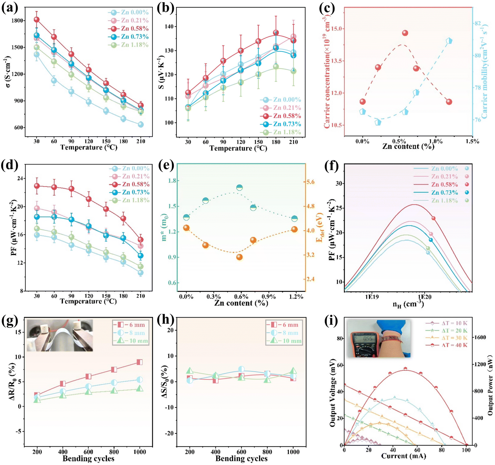 | ||
| Fig. 5 Temperature-dependent (a) electrical conductivity σ, (b) Seebeck coefficient S, and (d) power factor (PF) of the Zn-doped Sb2Te3 samples; (c) carrier concentration (n) and carrier mobility (μ) of the Zn-doped Sb2Te3 samples with increasing Zn content; (e) the effective mass (m*) and deformation potential (Edef) with increasing Zn content calculated by the SPB model; (f) room-temperature fitted curves of the PF values as a function of n with the experimental PF values of the Zn-doped Sb2Te3 samples; the variation of (g) ΔR/R0 and (h) S after different bending times; (i) the output voltage and output power of the fabricated f-TEGs with the increase in current (I). | ||
To investigate the mechanical flexibility of the synthesized Zn-doped Sb2Te3 thin films, the variation of resistance (R) and S is recorded after bending several times. The variation of R is usually recorded as the resistance change rate (ΔR/R0, where ΔR is the difference of the initial resistance and resistance after bending, and R0 is the initial resistance). Fig. 5(g) and (h) illustrate the ΔR/R0 and S after bending several times with 6 mm, 8 mm, 10 mm bending radii by using custom-made bending furniture. The inset photo of Fig. 5(h) is the bending process conducted in the bending furniture. The error bars of both ΔR/R0 and S are 5% according to the measurement errors of the equipment. As shown in Fig. 5(g), the ΔR/R0 increased with the decrease in bending radius after bending 1000 times. The ΔR/R0 is 9%, 5%, and 3.8% when the bending radius is 6 mm, 8 mm, and 10 mm, respectively after bending 1000 times. As sgown in Fig. 5(h), all the S values after bending 1000 times are located at around 110 μV K−1. Thus, bending of the thin film does not introduce cracks or fractures and further influence S, since S is one of the intrinsic properties of the material itself. Therefore, the synthesis of Zn-doped Sb2Te3 thin films leads to outstanding mechanical properties and mechanical durability on a flexible PI substrate. Finally, the Zn 0.58% sample served as the p-leg for f-TEG device fabrication, characterized by using home-made equipment in our previous work. The measured output voltage U and output power P of this device as a function of current (I) with temperature difference ΔT are shown in Fig. 5(i). The U and P were measured by different ΔT values of 10 K, 20 K, 30 K, and 40 K. The maximum U and P reached ∼53.0 mV and ∼1100 nW under a ΔT of 40 K. These results can support that the synthesized f-TEG has great potential for application in self-powered wearable devices.
4. Conclusion
In this work, we identified the appropriate dopant of Zn with the support of theoretical calculations and then successfully synthesized the Zn-doped p-type Sb2Te3 flexible thin films. The DFT calculation of the band structure indicates the shift of the Fermi-level to the top of the valence band by enhancing the hole concentration, and also confirms the significant dopant of Zn among all the p-type doping dopants. The thin film samples were all synthesized by a directional thermal diffusion method, which was thermally connected by the Sb/Zn precursor film (magnetron sputtering method) and Te film (thermal evaporation method). Microstructure characterization showed that the dopant Zn atoms have entered the lattice of Sb2Te3 by XRD, XPS, SEM, EDS, and TEM results, and Zn replaces the Sb sites. Consequently, the σ was enhanced by the improvement of n; however, the S was most likely to be improved by the increase in m*, achieving the decoupling of S and σ in Zn-doped Sb2Te3 thin films. Meanwhile, the synthesized thin films are proved to possess outstanding mechanical flexibility and durability after bending tests. Finally, a significantly high power factor value of 22.93 μW cm−1 K−2 at room temperature in the Zn 0.58% sample was achieved. Thus, this work provides a mature synthesis procedure and significant theoretical calculation guidance for the Sb2Te3 thin film to reach the demand of wearable F-TEGs.Data availability
All data that support the findings of this study are available from the corresponding author upon reasonable request.Author contributions
Zilong Zhang: writing – original draft, data curation, conceptualization. Wenyu Yang: writing – original draft, formal analysis, conceptualization. Mohammad Nisar: methodology, investigation. Bo Wu: investigation, formal analysis. Fu Li: formal analysis, data curation. Guangxing Liang: writing – review & editing. Jingting Luo: methodology, formal analysis. Yuexing Chen: funding acquisition, formal analysis. Zhuanghao Zheng: supervision.Conflicts of interest
There are no conflicts of interest to declare.Acknowledgements
Z. L. Zhang and W. Y. Yang contributed equally. This work was supported by the National Natural Science Foundation of China (62274112), the National Natural Science Foundation of Guangdong province of China (2024B1515020119 and 2022A1515010929), and the Science and Technology Plan Project of Shenzhen (JCYJ20220531103601003).References
- P. P. Murmu, A. Shettigar, S. V. Chong, Z. Liu, D. Goodacre, V. Jovic, T. Mori, K. E. Smith and J. Kennedy, J. Materiomics, 2021, 7, 612–620 CrossRef
.
-
D. M. Rowe, Thermoelectrics Handbook: Macro to Nano, CRC press, 2018 Search PubMed
- L. Miao, S. Zhu, C. Liu, J. Gao, Z. Zhang, Y. Peng, J. L. Chen, Y. Gao, J. Liang and T. Mori, Nat. Commun., 2024, 15, 8516 CrossRef CAS PubMed
- N. Jia, J. Cao, X. Y. Tan, J. Dong, H. Liu, C. K. I. Tan, J. Xu, Q. Yan, X. J. Loh and A. Suwardi, Mater. Today Phys., 2021, 21, 100519 CrossRef CAS
- J. Kennedy, P. P. Murmu, P. Kumar and G. Ramanath, Mater. Res. Bull., 2021, 142, 111426 CrossRef CAS
- T. M. Tritt and M. Subramanian, MRS Bull., 2006, 31, 188–198 CrossRef
- Y. Xiao and L. D. Zhao, Science, 2020, 367, 1196–1197 CrossRef CAS PubMed
- N. Kuang, Z. Zuo, W. Wang, R. Liu and Z. Zhao, Sens. Actuators, A, 2021, 332, 113030 CrossRef CAS
- K. Singkaselit, A. Sakulkalavek and R. Sakdanuphab, Adv. Nat. Sci.:Nanosci. Nanotechnol., 2017, 8, 035002 Search PubMed
- T. Cao, X. L. Shi and Z.-G. Chen, Prog. Mater. Sci., 2023, 131, 101003 CrossRef CAS
- P. Dharmaiah, H. S. Kim, C. H. Lee and S. J. Hong, J. Alloys Compd., 2016, 686, 1–8 CrossRef CAS
- B. Poudel, Q. Hao, Y. Ma, Y. Lan, A. Minnich, B. Yu, X. Yan, D. Wang, A. Muto and D. Vashaee, Science, 2008, 320, 634–638 CrossRef CAS PubMed
- J. Son, M. Oh, B. Kim, S. Park, B. Min, M. Kim and H. Lee, J. Alloys Compd., 2013, 566, 168–174 CrossRef CAS
- L. M. Goncalves, P. Alpuim, A. G. Rolo and J. H. Correia, Thin Solid Films, 2011, 519, 4152–4157 CrossRef CAS
- M. Wei, X. L. Shi, Z. H. Zheng, F. Li, W. D. Liu, L. P. Xiang, Y. S. Xie, Y. X. Chen, J. Y. Duan and H. L. Ma, Adv. Funct. Mater., 2022, 32, 2207903 CrossRef CAS
- D. W. Ao, W. D. Liu, Z. H. Zheng, X. L. Shi, M. Wei, Y. M. Zhong, M. Li, G. X. Liang, P. Fan and Z. G. Chen, Adv. Energy Mater., 2022, 12, 2202731 CrossRef CAS
- O. Yamashita, S. Tomiyoshi and K. Makita, J. Appl. Phys., 2003, 93, 368–374 CrossRef CAS
- R. J. Mehta, Y. Zhang, H. Zhu, D. S. Parker, M. Belley, D. J. Singh, R. Ramprasad, T. Borca-Tasciuc and G. Ramanath, Nano Lett., 2012, 12, 4523–4529 CrossRef CAS PubMed
- S. I. Kim, K. H. Lee, H. A. Mun, H. S. Kim, S. W. Hwang, J. W. Roh, D. J. Yang, W. H. Shin, X. S. Li, Y. H. Lee, G. J. Snyder and S. W. Kim, Science, 2015, 348, 109–114 CrossRef CAS PubMed
- E. M. Vieira, J. Figueira, A. L. Pires, J. Grilo, M. F. Silva, A. M. Pereira and L. M. Goncalves, J. Alloys Compd., 2019, 774, 1102–1116 CrossRef CAS
- D. W. Newbrook, S. P. Richards, V. K. Greenacre, A. L. Hector, W. Levason, G. Reid, C. K. de Groot and R. Huang, ACS Appl. Energy Mater., 2020, 3, 5840–5846 CrossRef CAS
- D. W. Ao, B. Wu, W. D. Liu, X. B. Shen and W. Q. Wei, Rare Met., 2024, 1–9 Search PubMed
- M. Wei, H. Li, M. Nisar, Z. Zhang, F. Li, G. Liang, J. Luo, Z. Zheng, Y. Chen and Z. Zheng, Chem. Eng. J., 2024, 153185 CrossRef CAS
- B. Yang, Y. Luo, C. Li, W. Li, C. Sun, Z. Ma, Y. Qian, X. Zeng, Y. Wei and H. Liu, Chem. Eng. J., 2023, 477, 147005 CrossRef CAS
- J. Kim, M. Zhang, W. Bosze, S. D. Park, J.-H. Lim and N. V. Myung, Nano Energy, 2015, 13, 727–734 CrossRef CAS
- N. Hatsuta, D. Takemori and M. Takashiri, J. Alloys Compd., 2016, 685, 147–152 CrossRef CAS
- M. Tan, W. D. Liu, X. L. Shi, J. Shang, H. Li, X. Liu, L. Kou, M. Dargusch, Y. Deng and Z.-G. Chen, Nano Energy, 2020, 78, 105379 CrossRef CAS
- Z. H. Zheng, Y. M. Zhong, Y. L. Li, M. Nisar, A. Mansoor, F. Li, S. Chen, G. X. Liang, P. Fan and D. Xu, Carbon Energy, 2024, e541 CrossRef CAS
- G. Kresse and D. Joubert, Phys. Rev. B, 1999, 59, 1758 CrossRef CAS
- J. P. Perdew, K. Burke and M. Ernzerhof, Phys. Rev. Lett., 1996, 77, 3865 CrossRef CAS PubMed
- J. P. Perdew, J. Chevary, S. Vosko, K. A. Jackson, M. R. Pederson, D. Singh and C. Fiolhais, Phys. Rev. B:Condens. Matter Mater. Phys., 1993, 48, 4978 CrossRef CAS PubMed
- Z. H. Zheng, X. L. Shi, D. W. Ao, W. D. Liu, M. Li, L. Z. Kou, Y. X. Chen, F. Li, M. Wei and G. X. Liang, Nat. Sustain., 2023, 6, 180–191 CrossRef
Footnote |
| † Electronic supplementary information (ESI) available. See DOI: https://doi.org/10.1039/d4sc07793h |
| This journal is © The Royal Society of Chemistry 2025 |