
 Open Access Article
 This Open Access Article is licensed under a Creative Commons Attribution-Non Commercial 3.0 Unported Licence
Buried interface management toward high-performance perovskite solar cells†
Bin
Du‡
 *a,
Yuexin
Lin‡
b,
Jintao
Ma
a,
Weidan
Gu
a,
Fei
Liu
a,
Yijun
Yao
*c and
Lin
Song
*d
*a,
Yuexin
Lin‡
b,
Jintao
Ma
a,
Weidan
Gu
a,
Fei
Liu
a,
Yijun
Yao
*c and
Lin
Song
*d
aSchool of Materials Science and Engineering, Xi'an Polytechnic University, Xi'an 710048, China. E-mail: dubin@xpu.edu.cn
bMOE Key Laboratory for Nonequilibrium Synthesis and Modulation of Condensed Matter, School of Physics, National Innovation Platform (Center) for Industry-Education Integration of Energy Storage Technology, Xi'an Jiaotong University, Xi'an 710049, P. R. China
cSchool of Textile Science and Engineering, Xi'an Polytechnic University, Xi'an, 710048, Shaanxi, China. E-mail: yaoyj@xpu.edu.cn
dFrontiers Science Center for Flexible Electronics (FSCFE), Institute of Flexible Electronics (IFE), Northwestern Polytechnical University, Xi'an 710072, China. E-mail: iamlsong@nwpu.edu.cn
First published on 18th December 2024
Abstract
The interface between the perovskite layer and the electron transport layer is an extremely important factor that cannot be ignored in achieving high-performance perovskite photovoltaic technology. However, the void defects of the interface pose a serious challenge for high performance perovskite solar cells (PSCs). To address this, we report a polydentate ligand reinforced chelating strategy to strengthen the stability of the buried interface by managing interfacial defects and stress. Gelatin-coupled cellulose (GCC) is employed to manipulate the buried interface. The unique functional groups in GCC synergistically passivate the defects from the surface of SnO2 and the bottom surface of the perovskite layer. Our work demonstrates that by implementing GCC as a buried interface strategy, it is possible to prepare devices with reduced vacancy states, non-radiative recombination suppression, and excellent optoelectronic performance. At the same time, this work improves the efficiency and stability of PSCs and provides greater space for device manufacturing.
1. Introduction
Perovskite solar cells (PSCs) have emerged as a research frontier of photovoltaic technologies with their excellent photovoltaic properties, including long carrier lifetimes, high light absorption coefficients, adjustable band gaps and high defect tolerance.1–5 So far, the highest certified power conversion efficiency (PCE) has exceeded 26%.6–10 However, long-term stability remains a major bottleneck for commercial application, which requires a product lifetime of approximately 20–25 years.11–15 For typical n–i–p PSCs, the electron transport layer (ETL) is an important component of PSCs, responsible for transporting electrons and blocking holes. How to fabricate high-quality ETLs with reduced defects is the key to achieve efficient and stable n–i–p PSCs.16–18 Through the interfaces between adjacent functional layers in PSCs photogenerated carriers complete the extraction, transport, and collection processes during the operation of PSCs.19 The favorable band alignment between the ETL and the perovskite film facilitates charge extraction, charge complex inhibition and long-term device stability.20 Therefore, the resulting performance of PSCs is closely related to the nature of these interfaces. Due to the inconsistent lattice constants of each functional layer within PSCs, defects at the interface tend to be more numerous than those in the perovskite bulk, leading to more severe non-radiative composites.21 As one of the most widely used ETL materials in n–i–p PSCs, tin oxide (SnO2) exhibits various advantages such as high electron mobility, high transmittance, and excellent photostability. Since the deposition of SnO2 is prearranged prior to the preparation of perovskite films in n–i–p structured PSCs, it dominates perovskite crystallization and interfacial charge transport.22–24 Therefore, high-quality SnO2 films are crucial for achieving high-performance PSCs, whereas generally for the surface of SnO2 films prepared by the sol–gel method, there are a large number of defects (e.g., oxygen and tin vacancies and interstitial and antisite defects), which can lead to charge accumulation and interfacial non-radiative recombination loss, limiting the photovoltaic performance and operational stability of PSCs.25,26 In addition, the imperfect band alignment between SnO2 and perovskite exacerbates the hysteresis-induced charge extraction block. The high efficiency of PSCs is achieved by increasing the charge transfer efficiency between the interfaces and reducing non-radiative compounding.27,28 Interfacial engineering aims to passivate interfacial defects or adjust the band alignment by introducing interface layers or improving the interfacial properties to reduce losses.29,30 Therefore, modification of the SnO2/perovskite interface has attracted the attention of many researchers as a simple and feasible strategy that can both passivate interfacial defects efficiently and connect the perovskite layer and lower functional layers, thus enabling the optimization of perovskite crystals at the same time.31–33In this work, gelatin-coupled cellulose (GCC) was first used to modify the SnO2/perovskite interface, which contributes to both interfacial modification and crystalline modulation. The results show that GCC can interact strongly with both SnO2 and perovskite layers, playing a bridge-like role at the buried interface to achieve the improvement of charge transfer and modulation of the energy level structure. Specifically, strong hydrogen bonds will form between –NH2/–NH3+ in GCC and I/I− in PbI2, which can anchor I− on the surface of SnO2 and promote the uniform growth of PbI2 and perovskite. On the other hand, the carbonyl groups in GCC can form chemical bonds with uncoordinated Pb2+ and reduce the bottom defects of the perovskite layer. In addition, cellulose contains a large number of hydroxyl groups that can coordinate with the uncoordinated Sn4+ in SnO2, thereby filling the oxygen vacancies in SnO2 thin films and passivating the surface defects of SnO2. Thus, more matched energy levels can be formed between SnO2, GCC and perovskite layers, which will help in electron extraction and transport. As a result, compared to the initial device (PCE of 21.68%), the GCC-modified device achieves a significant enhancement of PCE to 25.06%. Moreover, the GCC-modified device maintains 91% of the initial PCE without encapsulation after aging under ambient conditions (25 °C, RH = 20–30%) for more than 1080 h. In contrast, the control device only retained 70% of its initial PCE. This excellent stability could be attributed to the high crystallinity of perovskite grains and the defect passivation of GCC between SnO2 and perovskite layers. This work has provided an opportunity to improve the perovskite film's crystal quality, reduce the grain boundary and SnO2 surface defects, modulate the energy level structure of SnO2, and improve the electron transfer ability in PSCs providing a feasible and effective interfacial modification strategy, while the combination of interfacial management and energy level control used for embedding provides new perspectives for achieving high-performance and stable and durable PSCs.
2. Results and discussion
Cellulose is a biological polymer containing plenty of hydroxyl groups, which can coordinate with uncoordinated Sn4+ so that the oxygen vacancy in the SnO2 film is filled, thereby passivating the surface defects of SnO2.34,35 In this paper, in order to enhance interfacial contact between SnO2 and the perovskite layer, modified cellulose, called GCC, has been synthesized (as shown in Fig. S1†), which introduces a small molecule cinnamyl chloride to react with hydroxyl groups of cellulose,36 aiming to anchor carbonyl groups in the side chain of cellulose. These carbonyl groups could form chemical bonds with uncoordinated Pb2+ and reduce the bottom imperfections of the perovskite layer.37,38 The schematic diagram of the mechanism is displayed in Fig. 1.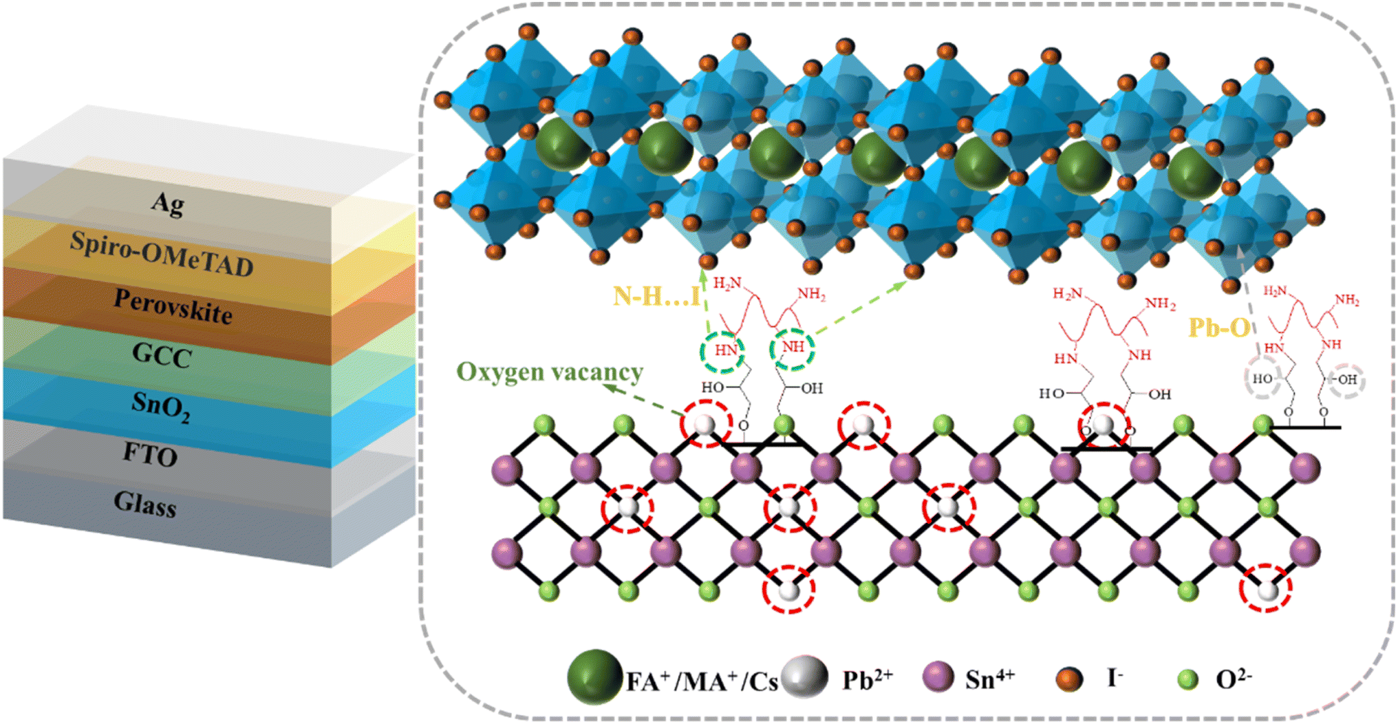 | ||
| Fig. 1 A schematic diagram of the modification mechanism of GCC at the ETL/perovskite interface is proposed. The chemical structure of the GCC molecule is shown in the middle of the diagram. | ||
To gain a deeper understanding of the mechanism between the SnO2 ETL and GCC, X-ray photoelectron spectroscopy (XPS) measurements were performed (as shown in Fig. S2†). As seen from the XPS result in Fig. 2a, the binding energies of Sn 3d3/2 (495.54 eV) and Sn 3d5/2 (487.13 eV) of SnO2 were both shifted to higher binding energies of 495.64 and 487.23 eV after modification with GCC, indicating the strong chemical interaction between the GCC interlayer and SnO2, which may result from the coordination between uncoordinated Sn4+ on the surface of SnO2 and hydroxyl in GCC molecules. The O 1s XPS spectra are shown in Fig. 2b and c. The O 1s characteristic peaks of the original SnO2 and SnO2/GCC films can be convoluted into two sub-peaks which are assigned to the lattice oxygen (OL) and oxygen vacancies (OV) in SnO2, respectively. OL represents the O2− ions combined with the adjacent metal ions in the lattice, and OV represents the O2− ions in the OV region. The OV content in the film can be estimated using the peak area (ROV) of OV. The concentrations of OV and OL can be represented by the corresponding area of OV and OL peaks. The ratio of OV (ROV) was calculated using the formula: ROV = SOV/(SOV + SOL), where SOV and SOL represent the peak area of OV and OL, respectively.39 After calculation, ROV was significantly reduced from 0.3495 (pristine SnO2) to 0.1242 (GCC-treated SnO2). The decrease in ROV represents the reduction of oxygen vacancies in the SnO2 film, indicating that GCC can passivate oxygen-deficient defects of SnO2 films.
 | ||
| Fig. 2 XPS high-resolution spectra of SnO2 and SnO2/GCC for (a) Sn 3d and (b) and (c) O 1s. XPS high-resolution spectra of SnO2/PbI2 and SnO2/GCC/PbI2 for (d) Pb 4f and (e) I 3d. (f) XPS full spectra of SnO2 and SnO2/GCC. | ||
To further study the effect of GCC on the perovskite layer, XPS measurements are also carried out to analyze the perovskite film based on pristine SnO2 and GCC-modified SnO2. As shown in the Pb 4f XPS spectrum in Fig. 2d, the perovskite crystal lattice produced two distinct Pb 4f peaks at 138.40 eV and 143.26 eV, which were attributed to Pb 4f7/2 and Pb 4f5/2, respectively. After GCC treatment, these two main peaks were shifted to higher binding energies at 138.47 eV and 143.36 eV, respectively, which was attributed to the reduction of electrons around Pb atoms when the carbonyl group in GCC electrostatically coupled with the uncoordinated Pb2+. This is due to the reduction of electrons around the Pb atoms when the carbonyl group in GCC is electrostatically coupled to the uncoordinated Pb2+ at the bottom of the perovskite film, which allows the Pb2+ defects in the perovskite film to be passivated effectively.40 Similarly, the electrons around the Pb atoms in the perovskite films attributed to I 3d5/2 and I 3d3/2 also increase from the initial 619.22 eV and 630.73 eV to 619.35 eV and 630.88 eV, respectively, as shown in Fig. 2e. This indicates that GCC also strongly interacts with I− in the perovskite, which reduces the migration of I− and effectively inhibits the formation of I2 defects. In addition, the increase in binding energy is due to the fact that I− can provide additional negative charge to fill the OV through electrostatic coupling, which also verifies the results of the O 1s XPS spectra. The XPS full spectra of SnO2 and SnO2/GCC thin films are shown in Fig. 2f. These XPS characterization results confirm that GCC can be used as an interfacial crosslinker to passivate the defects on the surface of SnO2 films as well as to interact with the bottom of the perovskite layer, which greatly enhances the interfacial contact between the SnO2 ETL and the perovskite film.
We perform ultraviolet photoelectron spectroscopy (UPS) to study the work function (WF) of SnO2 films before and after modification to explain the effect of introducing GCC on the interface energy level structure. Fig. 3a shows the UPS spectra of SnO2 and SnO2/GCC thin films, respectively. The high binding energy edges and low binding energy edges on both sides of the UPS spectrum are referred to as the cut-off edge (Ecutoff) and Fermi edge (EF,edge), respectively.41Fig. 3b and c show the Ecutoff and EF,edge of SnO2 and SnO2/GCC thin films characterized by UPS, respectively. The Ecutoff of SnO2 and SnO2/GCC is 16.61 eV and 16.57 eV, and the EF,edge is 3.92 eV and 3.73 eV, respectively. Fig. 3d shows a Tauc plot converted from relevant UV-Vis spectra, from which the band gaps of SnO2 and SnO2/GCC thin films were fitted to be 3.90 eV, indicating that the introduction of GCC did not change the band gap of SnO2 thin films. Fig. S3† show UPS spectra of SnO2/perovskite film. The Fermi levels of different thin films can be calculated using the formula42

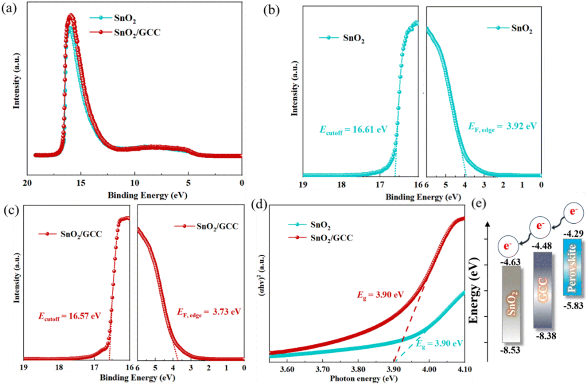 | ||
| Fig. 3 (a) UPS full spectra of SnO2 and SnO2/GCC. UPS spectra of (b) SnO2 film and (c) SnO2/GCC film. (d) Tauc-plot spectra of perovskite films deposited on SnO2 and SnO2/GCC substrates. (e) The energy level diagram of SnO2, SnO2/GCC, and perovskite. | ||
After calculation, the Fermi level values of SnO2 and SnO2/GCC are −4.61 eV and −3.65 eV, respectively. The valence-band energy level (EVB) values are calculated to be −8.53 eV and −8.38 eV, respectively. The conduction-band energy level (ECB) values are −4.63 eV and −4.48 eV, respectively. Therefore, the detailed energy level diagrams of SnO2 and SnO2/GCC are shown in Fig. 3e. It can be observed that SnO2 and SnO2/GCC achieve a stepped energy level arrangement, and significant downward band bending occurs at the GCC modified interface. This is beneficial for improving unipolar charge extraction and suppressing interface recombination, promoting electron extraction and transport, and greatly reducing VOC losses in PSCs, improving the electron collection efficiency of PSC cathodes for charge carriers. Table S1† provides detailed parameters of the energy levels of SnO2 and SnO2/GCC.
In order to investigate the effect of GCC interface introduction on the morphology of perovskite films, we characterized the perovskite films deposited on the SnO2 ETL and SnO2/GCC ETL using an optical microscope (OM), a scanning electron microscope (SEM) and atomic force microscopy (AFM), respectively, and studied the effect of the GCC bridging interlayer on the morphology of the upper perovskite. The OM test results in Fig. S5† indicate that the perovskite film deposited on the control group SnO2 film has obvious pinholes, while the perovskite film grown on the SnO2/GCC ETL has higher quality and no obvious pinholes. The SEM image in Fig. 4a shows that compared to the original film, the grain size of the perovskite film grown on the SnO2/GCC ETL significantly increases, which may be attributed to the interaction between carbonyl groups and PbI2 in GCC, resulting in slow crystal growth. Larger grain size and improved morphology facilitate charge transfer and reduce energy loss of PSCs caused by defects. The AFM image in Fig. 4b shows that the perovskite film formed after GCC modification exhibits a pinhole free morphology, and the root mean square (RMS) roughness also decreases from 37.19 nm of the original SnO2 film to 24.64 nm. In addition, Fig. S4† also illustrates the role of GCC. This result supports the conclusion of SEM measurement, proving that GCC can effectively optimize the morphology of perovskite films and improve film quality. High quality perovskite films are more conducive to reducing electron transport pathways and enhancing carrier transport capabilities. Fig. 4c shows the X-ray diffraction (XRD) patterns of perovskite films grown on different ETL substrates, and the crystallization properties of perovskite films were analyzed through XRD testing. The two typical diffraction peaks at 14.2° and 28.2° that significantly appear in both the original film and the modified film are attributed to the (110) and (220) crystal planes that dominate crystallinity and stability in perovskite, respectively. For GCC modified thin films, the intensities of the (110) and (220) crystal plane peaks are higher, which further indicates that introducing GCC on SnO2 can promote the crystal growth of perovskite. This result is consistent with the results of SEM and AFM images.
 | ||
| Fig. 4 (a) SEM and (b) AFM images of perovskite films deposited on SnO2 and SnO2/GCC ETLs. (c) XRD patterns of perovskite films. (d) 2D-GIWAXS images, and (e) derived 1D integral analysis spectra of the perovskite films deposited on SnO2 and SnO2/GCC ETLs. | ||
In order to further investigate the crystal structure and orientation of GCC modified perovskite films, we performed the grazing incidence angle wide-angle X-ray scattering (GIWAXS) test of perovskite films deposited on different ETL substrates in different dimensions (Fig. 4d and e). From the two-dimensional (2D) image in Fig. 4d, it can be seen that the SnO2/GCC ETL based perovskite film exhibits a typical three-dimensional (3D) perovskite structure. Typical scattering rings corresponding to the (110) and (220) crystal planes of perovskite can be clearly observed at q ≈ 1 Å−1 and q ≈ 2 Å−1. Then, we conducted one-dimensional (1D) integration analysis on the 2D diffraction pattern around the perovskite (110) crystal plane to more clearly quantify the difference in crystallinity of the film before and after modification, as shown in Fig. 4e. It is worth noting that compared with the SnO2 ETL substrate, the perovskite film based on the SnO2/GCC ETL exhibits the strongest (110) diffraction peak intensity at q = 1.01 Å−1, which will lead to better crystal orientation of the perovskite film and fully reflect the XRD spectrum results, indicating that perovskite films grown on SnO2/GCC ETL substrates have higher crystallinity.
The optimized surface energy level and improved perovskite film quality will affect the dynamic transport and recombination of interface carriers. To further study the effect of GCC on the charge transfer and carrier extraction process of the perovskite layer, we characterized the steady-state photoluminescence (PL) spectra and time-resolved photoluminescence (TRPL) spectra of perovskite films on SnO2 and SnO2/GCC substrates, respectively. Fig. 5a shows the steady-state PL spectra of the perovskite layers on different substrates. The PL intensity indicates the carrier recombination rate of the perovskite film. For all thin film samples, the emitted light is incident from the side of the perovskite film. A strong PL peak at 796 nm can be clearly observed in the perovskite film deposited on the original SnO2 ETL. However, for the GCC modified samples, the intensity of the PL peak at the same position was significantly reduced. This result indicates that a more efficient electron extraction process occurred between SnO2 and perovskite thin films, due to the strong chemical interactions between GCC and the perovskite and SnO2 layers, which is consistent with the results of XPS. The Kelvin probe force microscope (KPFM) measurement is also used to visualize the surface potential of the SnO2 film. The surface potential of the modified film (Fig. 5c) is significantly higher than that of the original (Fig. 5b), indicating that the introduction of GCC can effectively modify the WF of the SnO2 film. Fig. 5d shows the TRPL decay curves of perovskite layers on different substrates. The fitted values are listed in Table S2.† This indicates that the introduction of GCC can promote the extraction and collection of charges at the interface, thereby increasing VOC.
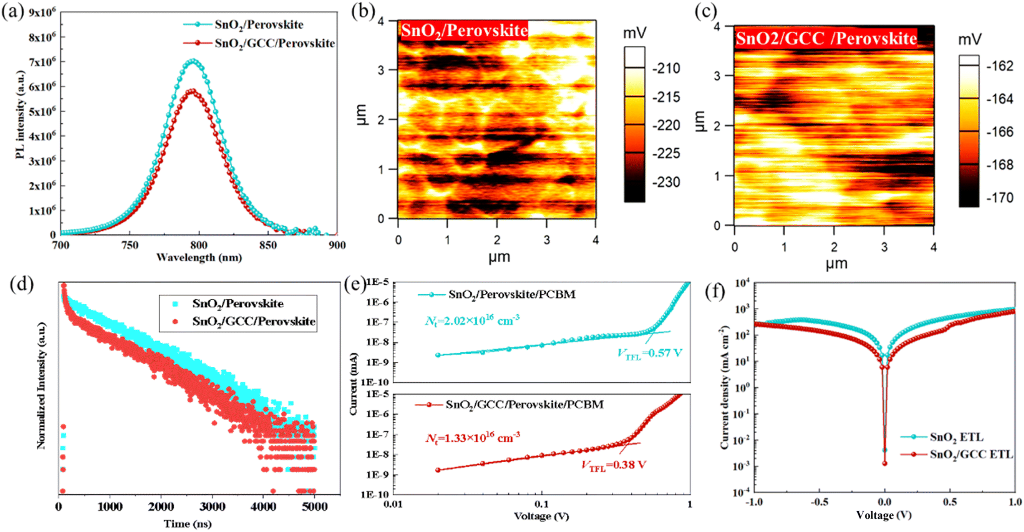 | ||
| Fig. 5 (a) PL spectra of the perovskite film deposited on ITO/SnO2 and ITO/SnO2/GCC. KPFM images of the perovskite film deposited on (b) ITO/SnO2 and (c) ITO/SnO2/GCC. (d) TRPL spectra of the perovskite film deposited on ITO/SnO2 and ITO/SnO2/GCC. (e) Dark I–V curve of the electron-only device with ITO/SnO2/perovskite/PCBM/Ag and ITO/SnO2/GCC/perovskite/PCBM/Ag structures. (f) Dark J–V curve of the devices with and without GCC treatment. | ||
To verify the carrier transport capacity at the modified SnO2/perovskite interface, we performed space charge limited current (SCLC) measurements. Fig. 5e shows the dark I–V curve of the ITO/SnO2 (or SnO2/GCC)/perovskite/[6,6]-phenyl-C61-butyric acid methyl ester (PCBM)/Ag pure electronic device. The curve is divided into a low-voltage region on the left and a trap-filling region on the right. At the same time, the voltage crossing point from the tangent of the ohmic region and the extension line of the trap-filling region is defined as the trap-filling limit voltage (VTFL). The trap state density (Nt) of the carrier can be calculated using the following equation:43

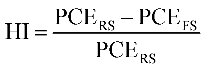
To study the effect of the GCC interface on the photovoltaic performance of the device, we measured the power output curves of PSCs with GCC modified SnO2 under standard AM 1.5 G illumination (Fig. 6a). It is worth noting that the GCC passivation layer plays a vital role in device performance. In detail, the control device based on the pure SnO2 ETL exhibits a champion PCE of 25.06% with a VOC of 1.17 V, a JSC of 25.59 mA cm−2, and an FF of 83.61%. Fig. 6b and Table S3† show the J–V curves of PSC devices with/without GCC modification measured by reverse scanning and forward scanning. The hysteresis phenomenon of PSCs is caused by ion migration due to the high density of defect states in the perovskite material and the imbalance of charge transport inside the PSC device. The hysteresis index (HI) is calculated using the equation:
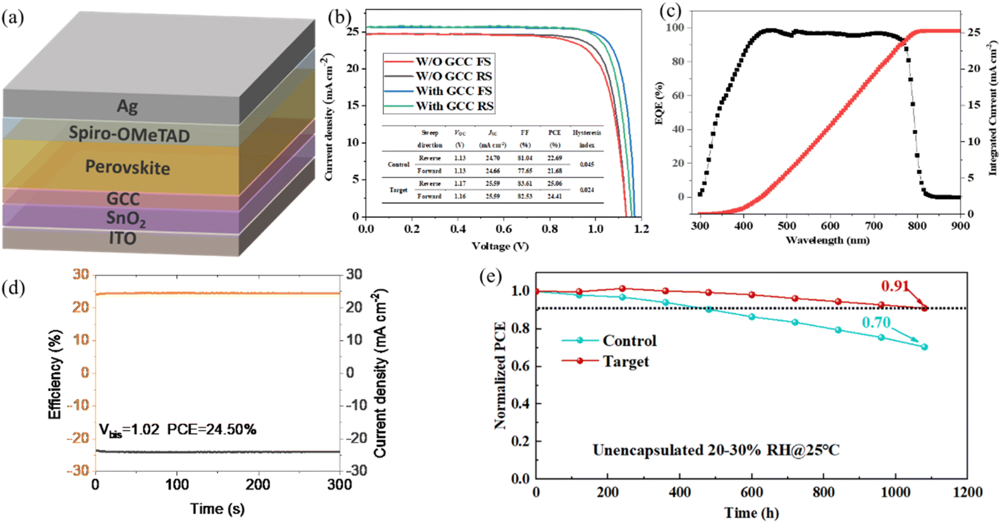 | ||
| Fig. 6 (a) Schematic illustration of an implemented PSC. (b) J–V curves of the PSC device with and without GCC treatments. (c) The EQE spectrum and integrated current of the PSC device after GCC passivation. (d) Steady-state power output curves of PSCs. (e) The environmental stability curves of the control and GCC-modified unencapsulated devices at 20–30% RH @ 25 °C. | ||
Compared with the control device, the HI of the device after GCC modification is significantly reduced from 0.045 to 0.024, indicating that the device defects are reduced, which further illustrates the hysteresis elimination effect of GCC on PSCs at the interface. Fig. S7† shows the I–V curves of devices based on SnO2 and SnO2/GCC ETLs. From the results, it can be seen that after the introduction of the GCC interface, the performance of PSCs prepared based on the SnO2/GCC ETL substrate was significantly enhanced under different scanning direction measurements. The external quantum efficiency (EQE) spectrum and integrated current of the device after GCC passivation are shown in Fig. 6c. The EQE measurement was performed to verify the reliability of JSC. By integrating the EQE data on the entire measurement spectrum of the GCC-modified device, the integrated JSC was calculated to be 25.59 mA cm−2, which was close to the value extracted from the J–V curve. The long-term stability of PSCs is the most important factor affecting their commercialization, so we finally studied the effect of GCC modification on the stability of PSCs. The steady-state power output is shown in Fig. 6d; the stable output PCE of the GCC-modified PSC after 300 s is 24.50%, indicating that GCC-modified PSCs can maintain stable output capability. Additionally, Fig. S9† shows the contact angle measurements of different ETLs. Fig. S10† shows the change in the contact GCC angle of the perovskite film before and after modification. The contact angle of the perovskite precursor based on the GCC-modified SnO2 film increases from 43° to 59°. This is due to the reaction between the carboxyl groups unique to GCC and the free hydroxyl defects on the surface of SnO2, which enhances the hydrophobicity of the perovskite film. Finally, we evaluated the environmental stability of unencapsulated PSCs. Additionally, the GCC-modified device exhibited a higher recombination resistance, as shown in Fig. S11,† which is beneficial for reducing carrier recombination and improving charge transport. Fig. S12† shows the statistical distribution of photovoltaic parameters for devices manufactured using SnO2 and SnO2/GCC. As shown in Fig. 6e, after continuously placing the control device and GCC-modified PSCs in ambient air for 1080 hours, the control device only retained 70% of its original PCE, while the GCC-modified device retained 91% of its original PCE. This good stability can be attributed to the high crystallinity of perovskite grains and the defect passivation of GCC between SnO2 and perovskite layers. These results strongly indicate that introducing GCC molecular bridges at the buried interface can reduce the risk of device degradation caused by external factors. As shown in Fig. S13,† the GCC modified device exhibits significantly enhanced long-term stability.
3. Conclusion
In summary, we have successfully demonstrated that GCC acts as a bidirectional cross-linking agent between the SnO2 ETL and the perovskite layer to simultaneously accelerate the extraction and transport of electrons at the buried interface and improve the crystal growth of perovskite films. Highly efficient and stable PSCs are achieved by interface energy level alignment and defect passivation. Finally, a high PCE of 25.06% can be achieved. In addition, after continuously placing the unencapsulated control group and GCC modified PSCs in ambient air (20–30% RH at 25 °C) for 1080 hours, the control group only retained 70% of its original PCE, while the GCC modified device retained 91% of its original PCE. It exhibits excellent operational stability. Our strategy provides simple and efficient and stable PSCs, thereby promoting the large-scale commercial application of PSCs.4. Experimental section
4.1 Materials
GCC was synthesised according to the previously published paper as follows. Chlorobenzene (CB), anisole, isopropanol (IPA), N,N-dimethylformamide (DMF), and dimethyl sulfoxide (DMSO) were purchased from Sigma-Aldrich. Lead iodide (PbI2) and cesium iodide (CsI) were obtained from Xi'an Polymer Light Technology Corp. Formamidinium iodide (FAI), methylammonium chloride (MACl) and lead methyl bromide (MAPbBr3) were purchased from Great Cell. Spiro-OMeTAD, 4-tert-butylpyridine (tBP) and lithium bis(trifluoromethanesulphonyl)imide (Li-TFSI) were purchased from Advanced Election Technology Co., Ltd.4.2 Device preparation
ITO (1.5 cm × 1.5 cm) was washed with deionized water containing detergent, ethanol, and isopropanol under ultrasonic treatment. The washing time is 15 min. After that, N2 is used for drying treatment, and then ultraviolet ozone is used for treatment. The treatment time is 40 min, resulting in a hydrophilic surface. The SnO2 solution was spin-coated on the ITO substrate at 4000 rpm, the time was 30 s, and then the annealing treatment was carried out under the conditions of ambient air at 150 °C, and the annealing time was 30 min. When the device is processed using GCC, the GCC solution is first spin-coated on the top of the ITO/SnO2 substrate and then rotated at a speed of 5000 rpm, the rotation time is 30 s, and then the perovskite layer is spin-coated. The sample was annealed at 100 °C in ambient air, and the annealing time was 5 min. After annealing, the device is moved into a glove box, and the perovskite film is prepared by a one-step anti-solvent spin coating method. To prepare a perovskite precursor solution, PbI2 (705.33 mg), FAI (233.54 mg), MAPbBr3 (18.20 mg), MACl (33.67 mg) and CsI (10.91 mg) were dissolved in a mixed solution of 1 mL DMF/DMSO (9![[thin space (1/6-em)]](https://www.rsc.org/images/entities/char_2009.gif) :1). The prepared perovskite precursor solution was spin-coated on the SnO2 film at a speed of 1000 rpm, and the spin-coating time was 10 s. After that, 300 μL of anisole was used to inject the SnO2 film at a speed of 4000 rpm for 20 s. Then, the device was removed from the glove box and annealed in ambient air at 100 °C.The annealing time is 40 min. After annealing, the device is placed into the glove box again and the HTL layer is spin-coated. Spiro-OMeTAD powder, tBP and Li-TFSI solution were added to CB, and then the spiro HTL solution was spin-coated on the perovskite film at a rate of 3000 rpm for 30 s. and oxidized in air; the oxidation time is 18 h. Finally, under high vacuum (<3.0 × 10⁻⁴ Pa), 100 nm of silver as the electrode was heated and evaporated.
:1). The prepared perovskite precursor solution was spin-coated on the SnO2 film at a speed of 1000 rpm, and the spin-coating time was 10 s. After that, 300 μL of anisole was used to inject the SnO2 film at a speed of 4000 rpm for 20 s. Then, the device was removed from the glove box and annealed in ambient air at 100 °C.The annealing time is 40 min. After annealing, the device is placed into the glove box again and the HTL layer is spin-coated. Spiro-OMeTAD powder, tBP and Li-TFSI solution were added to CB, and then the spiro HTL solution was spin-coated on the perovskite film at a rate of 3000 rpm for 30 s. and oxidized in air; the oxidation time is 18 h. Finally, under high vacuum (<3.0 × 10⁻⁴ Pa), 100 nm of silver as the electrode was heated and evaporated.
4.3 Characterization
J–V scans were performed with a Keithley 2400 Source Meter under simulated AM 1.5 G illumination at one sun (100 mW cm−2) using a solar simulator (EnliTech SS-F5-3A), and light intensities were calibrated using a silicon reference solar cell. The measurements were conducted in a glove box with a concentration of less than 0.1 ppm of oxygen and water. The devices were tested in reverse scan (1.2 V → −0.2 V, step 0.02 V) and forward scan (−0.2 V → 1.2 V, step 0.02 V). For the stability test, the devices were stored under indoor light illumination. The EQE spectrum was measured at room temperature in air with a QTEST HIFINITY 5 (Crowntech Inc., USA). The light intensity was calibrated using a standard single-crystal Si photovoltaic cell. The SEM measurements were performed using a Hitachi S-4800 electron microscope. The XRD patterns were analyzed using a Rigaku-D/Max-3A X-ray diffractometer with monochromatic Cu Kα irradiation (λ = 1.5406 Å). The GIWAXS measurements were performed at the BL14B1 beamline of the Shanghai Synchrotron Radiation Facility (SSRF) with an X-ray wavelength of 1.24 Å. The X-ray beam size was approximately 0.2 × 0.3 mm2, characterized by horizontal and vertical slits. The UV/Vis transmittance spectrum was measured with a UV/Vis spectrophotometer (U-3900H, Hitachi High-tech Co., Ltd). The TRPL and PL measurements were performed on an FLS1000. The XPS and UPS measurements were performed using a Kratos Axis Supra photoelectron spectrometer with a monochromatic source of Al (Kα) (1486.6 eV) X-rays. The AFM and KPFM images were captured using a Dimension Icon atomic force microscope.Data availability
The data supporting this article have been included as part of the ESI.†Author contributions
B. D., Y. Y. and L. S. designed the research. Y. L. and J. M. performed syntheses and measurements. W. G. and F. L. analyzed the data. B. D. and Y. L. wrote the manuscript.Conflicts of interest
The authors declare no competing financial interests.Acknowledgements
This work was financially supported by the Doctoral Research Start-up Project of Xi'an Polytechnic University (107020579), the Shaanxi Natural Science Foundation of China (2023-JC-QN-0680), the National Natural Science Foundation of China (52402055), the Science and Technology Plan Project of Xi'an City (23GXFW0015), the National Natural Science Foundation of China (52203125), the Innovation Capability Support Program of Shaanxi (2024ZC-KJXX-044), and the Taishan Industrial Experts Programme (tscx202312119).References
- H. Lu, Y. Liu, P. Ahlawat, A. Mishra, W. R. Tress, F. T. Eickemeyer, Y. Yang, F. Fu, Z. Wang, C. E. Avalos, B. I. Carlsen, A. Agarwalla, X. Zhang, X. Li, Y. Zhan, S. M. Zakeeruddin, L. Emsley, U. Rothlisberger, L. Zheng, A. Hagfeldt and M. Grätzel, Science, 2020, 370, 74 CrossRef.
- J. H. Noh, S. H. Im, J. H. Heo, T. N. Mandal and S. I. Seok, Nano Lett., 2013, 13, 1764–1769 CrossRef CAS.
- D. P. McMeekin, G. Sadoughi, W. Rehman, G. E. Eperon, M. Saliba, M. T. Hörantner, A. Haghighirad, N. Sakai, L. Korte, B. Rech, M. B. Johnston, L. M. Herz and H. J. Snaith, Science, 2016, 351, 151–155 CrossRef CAS PubMed.
- S. D. Stranks, G. E. Eperon, G. Grancini, C. Menelaou, M. J. Alcocer, T. Leijtens, L. M. Herz, A. Petrozza and H. J. Snaith, Science, 2013, 342, 341–344 CrossRef CAS.
- W. J. Yin, T. Shi and Y. Yan, Adv. Mater., 2014, 26, 4653–4658 CrossRef CAS.
- K. He, J. Zhang, X. Zhao, F. Liu, R. Chen, J. Ma, B. Du, Y. Wang and L. Song, J. Mater. Chem. A, 2024, 12, 19310–19320 RSC.
- G. Wang, L. Liao, L. Niu, L. Chen, W. Li, C. Xu, E. Mbeng, Y. Yao, D. Liu and Q. Song, Nanoscale, 2019, 11, 12108–12115 RSC.
- Q. Cao, T. Wang, X. Pu, X. He, M. Xiao, H. Chen, L. Zhuang, Q. Wei, H.-L. Loi, P. Guo, B. Kang, G. Feng, J. Zhuang, G. Feng, X. Li and F. Yan, Adv. Mater., 2024, 36, 2311970 CrossRef CAS.
- C. Zuo, L. Tan, H. Dong, J. Chen, F. Hao, C. Yi and L. Ding, DeCarbon, 2023, 2, 100020 CrossRef.
- X. Zhu, M. Du, J. Feng, H. Wang, Z. Xu, L. Wang, S. Zuo, C. Wang, Z. Wang, C. Zhang, X. Ren, S. Priya, D. Yang and S. F. Liu, Angew. Chem., Int. Ed., 2021, 60, 4238–4244 CrossRef CAS PubMed.
- J. Ma, L. Wang, K. He, Y. Sun, B. Li, Q. Zhao and B. Du, J. Mater. Chem. C, 2024, 12, 10837–10856 RSC.
- J. Zhang, W. Li, X. Lv, Y. Ji, W. Huang, T. Bu, Z. Ren, C. Yao, F. Huang, Y.-B. Cheng and J. Tong, Sol. RRL, 2024, 8, 2400184 CrossRef CAS.
- D. B. Khadka, Y. Shirai, M. Yanagida, H. Ota, A. Lyalin, T. Taketsugu and K. Miyano, Nat. Commun., 2024, 15, 882 CrossRef CAS PubMed.
- Z.-R. Lan, Y.-D. Wang, J.-Y. Shao, D.-X. Ma, Z. Liu, D. Li, Y. Hou, J. Yao and Y.-W. Zhong, Adv. Funct. Mater., 2024, 34, 2312426 CrossRef CAS.
- X. Kong, Z. Li, Y. Jiang, Z. Xu, S.-P. Feng, G. Zhou, J.-M. Liu and J. Gao, Surface. Interfac., 2021, 25, 101163 CrossRef CAS.
- J. Zhuang, P. Mao, Y. Luan, N. Chen, X. Cao, G. Niu, F. Jia, F. Wang, S. Cao and J. Wang, Adv. Funct. Mater., 2021, 31, 2010385 CrossRef CAS.
- Y. Zhang, L. Xu, Y. Wu, Q. Zhou, Z. Shi, X. Zhuang, B. Liu, B. Dong, X. Bai, W. Xu, D. Zhou and H. Song, Nano Energy, 2021, 90, 106610 CrossRef CAS.
- H. Min, D. Y. Lee, J. Kim, G. Kim, K. S. Lee, J. Kim, M. J. Paik, Y. K. Kim, K. S. Kim, M. G. Kim, T. J. Shin and S. I. Seok, Nature, 2021, 598, 444–450 CrossRef CAS PubMed.
- J. Zhang, B. Yu, Y. Sun and H. Yu, Adv. Energy Mater., 2023, 13, 2300382 CrossRef CAS.
- J. Park, J. Kim, H.-S. Yun, M. J. Paik, E. Noh, H. J. Mun, M. G. Kim, T. J. Shin and S. I. Seok, Nature, 2023, 616, 724–730 CrossRef CAS PubMed.
- J. Wang, S. Luo, X. Tang, S. Xiao, Z. Chen, S. Pang, L. Zhang, Y. Lin, J. He and Y. Yuan, ACS Energy Lett., 2021, 6, 3634–3642 CrossRef CAS.
- T. Wu, L. K. Ono, R. Yoshioka, C. Ding, C. Zhang, S. Mariotti, J. Zhang, K. Mitrofanov, X. Liu, H. Segawa, R. Kabe, L. Han and Y. Qi, Energy Environ. Sci., 2022, 15, 4612–4624 RSC.
- K. Wei, L. Yang, J. Deng, Z. Luo, X. Zhang and J. Zhang, ACS Appl. Energy Mater., 2022, 5, 7458–7465 CrossRef CAS.
- J. Chen and N.-G. Park, ACS Energy Lett., 2020, 5, 2742–2786 CrossRef CAS.
- Z.-W. Gao, Y. Wang and W. C. H. Choy, Adv. Energy Mater., 2022, 12, 2104030 CrossRef CAS.
- J. Chen, X. Zhao, S.-G. Kim and N.-G. Park, Adv. Mater., 2019, 31, 1902902 CrossRef.
- Q. Jiang, Y. Zhao, X. Zhang, X. Yang, Y. Chen, Z. Chu, Q. Ye, X. Li, Z. Yin and J. You, Nat. Photonics, 2019, 13, 460–466 CrossRef CAS.
- Y. Zhao, F. Ma, Z. Qu, S. Yu, T. Shen, H.-X. Deng, X. Chu, X. Peng, Y. Yuan, X. Zhang and J. You, Science, 2022, 377, 531–534 CrossRef CAS.
- X. Liang, M. Singh, F. Wang, P. W. K. Fong, Z. Ren, X. Zhou, X. Wan, C. M. Sutter-Fella, Y. Shi, H. Lin, Q. Zhu, G. Li and H. Hu, Adv. Sci., 2024, 11, 2305572 CrossRef CAS PubMed.
- Q. Zhuang, C. Zhang, C. Gong, H. Li, H. Li, Z. Zhang, H. Yang, J. Chen and Z. Zang, Nano Energy, 2022, 102, 107747 CrossRef CAS.
- J. Chen and W. C. H. Choy, Sol. RRL, 2020, 4, 2000408 CrossRef CAS.
- X. Ji, L. Bi, Q. Fu, B. Li, J. Wang, S. Y. Jeong, K. Feng, S. Ma, Q. Liao, F. R. Lin, H. Y. Woo, L. Lu, A. K. Y. Jen and X. Guo, Adv. Mater., 2023, 35, 2303665 CrossRef CAS.
- S. Zhang, M. Li, H. Zeng, X. Zheng, L. Luo, S. You, Y. Zhao, R. Liu, C. Tian and X. Li, ACS Energy Lett., 2022, 7, 3958–3966 CrossRef CAS.
- Y. Zhang, T. Kong, H. Xie, J. Song, Y. Li, Y. Ai, Y. Han and D. Bi, ACS Energy Lett., 2022, 7, 929–938 CrossRef CAS.
- C. Wang, J. Wu, S. Wang, Z. Yan, X. Liu, G. Li, L. Chen, S. Zhu, W. Sun and Z. Lan, Sol. RRL, 2022, 6, 2100995 CrossRef CAS.
- Z. Zhang, B. Zhang, N. Grishkewich, R. Berry and K. C. Tam, Adv. Sustainable Syst., 2019, 3, 1800156 CrossRef CAS.
- X. Li, W. Sheng, X. Duan, Z. Lin, J. Yang, L. Tan and Y. Chen, ACS Appl. Mater. Interfaces, 2022, 14, 34161–34170 CrossRef CAS.
- L. Yang, M. Wu, F. Cai, P. Wang, R. S. Gurney, D. Liu, J. Xia and T. Wang, J. Mater. Chem. A, 2018, 6, 10379–10387 RSC.
- X. Zuo, B. Kim, B. Liu, D. He, L. Bai, W. Wang, C. Xu, Q. Song, C. Jia, Z. Zang, D. Lee, X. Li and J. Chen, Chem. Eng. J., 2022, 431, 133209 CrossRef CAS.
- L. Yin, C. Ding, C. Liu, C. Zhao, W. Zha, I. Z. Mitrovic, E. G. Lim, Y. Han, X. Gao, L. Zhang, H. Wang, Y. Li, S. Wilken, R. Österbacka, H. Lin, C.-Q. Ma and C. Zhao, Adv. Energy Mater., 2023, 13, 2301161 CrossRef CAS.
- J.-W. Lee, H.-S. Kim and N.-G. Park, Acc. Chem. Res., 2016, 49, 311–319 CrossRef CAS PubMed.
- W. Hui, X. Kang, B. Wang, D. Li, Z. Su, Y. Bao, L. Gu, B. Zhang, X. Gao, L. Song and W. Huang, Nano Lett., 2023, 23, 2195–2202 CrossRef CAS PubMed.
- Z. Wang, Y. Lu, Z. Xu, J. Hu, Y. Chen, C. Zhang, Y. Wang, F. Guo and Y. Mai, Adv. Sci., 2021, 8, 2101856 CrossRef CAS.
Footnotes |
| † Electronic supplementary information (ESI) available. See DOI: https://doi.org/10.1039/d4sc06932c |
| ‡ Authors share equal authorship. |
| This journal is © The Royal Society of Chemistry 2025 |