
 Open Access Article
 This Open Access Article is licensed under a Creative Commons Attribution-Non Commercial 3.0 Unported Licence
Synthesis of shape-tunable PbZrTiO3 nanocrystals with lattice variations for piezoelectric energy harvesting and human motion detection†
Ya-Ju
Chuang‡
a,
Arnab
Pal‡
 b,
Bo-Hao
Chen
ac,
Satyaranjan
Jena
a,
Sreerag
Suresh
d,
Zong-Hong
Lin
*be and
Michael H.
Huang
*a
b,
Bo-Hao
Chen
ac,
Satyaranjan
Jena
a,
Sreerag
Suresh
d,
Zong-Hong
Lin
*be and
Michael H.
Huang
*a
aDepartment of Chemistry, National Tsing Hua University, Hsinchu 300044, Taiwan. E-mail: hyhuang@mx.nthu.edu.tw
bDepartment of Biomedical Engineering, National Taiwan University, Taipei 10617, Taiwan. E-mail: zhlin@ntu.edu.tw
cNational Synchrotron Radiation Research Center, Hsinchu 300092, Taiwan
dInstitute of NanoEngineering and MicroSystems, National Tsing Hua University, Hsinchu 300044, Taiwan
eDepartment of Power Mechanical Engineering, National Tsing Hua University, Hsinchu 300044, Taiwan
First published on 13th January 2025
Abstract
PbZr0.7Ti0.3O3 cubes with tunable sizes and cuboids have been hydrothermally synthesized. PbZrTiO3 cubes with three different Zr![[thin space (1/6-em)]](https://www.rsc.org/images/entities/char_2009.gif) :Ti atomic percentages were also prepared. Analysis of synchrotron X-ray diffraction (XRD) patterns reveals the presence of two lattice components for these samples. Fast Fourier Transform (FFT) processing of high-resolution transmission electron microscopy (HR-TEM) images shows discernible lattice spot differences between the inner bulk and surface layer region for a PbZr0.7Ti0.3O3 cube, while a cuboid has distinct lattice spot deviations. The lattice variations yield different dielectric constant numbers for these two samples, despite being bound by the same crystal faces. The PbZrTiO3 crystals give size- and composition-dependent band gaps. Cuboids show notably larger piezoelectric and ferroelectric responses than cubes. Piezoelectric nanogenerators (PENGs) containing 30 wt% cuboids produce the highest open-circuit voltage of 20.36 V and short-circuit current of 2300 nA. The PENGs harvest energy through bending/releasing cycles to power devices and show photothermal pyroelectric activity. Moreover, a single 30 wt% cuboid PENG device integrated into a shoe insole can deliver an impressive 96.8% accuracy for human motion detection using a machine learning approach. This work illustrates that considerable lattice variation through crystal shape control is effective in enhancing material properties.
:Ti atomic percentages were also prepared. Analysis of synchrotron X-ray diffraction (XRD) patterns reveals the presence of two lattice components for these samples. Fast Fourier Transform (FFT) processing of high-resolution transmission electron microscopy (HR-TEM) images shows discernible lattice spot differences between the inner bulk and surface layer region for a PbZr0.7Ti0.3O3 cube, while a cuboid has distinct lattice spot deviations. The lattice variations yield different dielectric constant numbers for these two samples, despite being bound by the same crystal faces. The PbZrTiO3 crystals give size- and composition-dependent band gaps. Cuboids show notably larger piezoelectric and ferroelectric responses than cubes. Piezoelectric nanogenerators (PENGs) containing 30 wt% cuboids produce the highest open-circuit voltage of 20.36 V and short-circuit current of 2300 nA. The PENGs harvest energy through bending/releasing cycles to power devices and show photothermal pyroelectric activity. Moreover, a single 30 wt% cuboid PENG device integrated into a shoe insole can deliver an impressive 96.8% accuracy for human motion detection using a machine learning approach. This work illustrates that considerable lattice variation through crystal shape control is effective in enhancing material properties.
Introduction
Semiconductor crystals broadly possess facet-dependent behaviors in their electrical conductivity, photocatalytic activity, and optical properties.1–8 Moreover, MnS and Co3O4 nanocrystals exhibit surface-specific magnetic properties.9,10 BaTiO3 cubes and octahedra also present appreciable differences in ferroelectric, piezoelectric, and pyroelectric responses.11 The emergence of all these phenomena should arise from the existence of bulk and surface region lattices with slight changes in their lattice constants, which are related to the particle shape or the exposed faces, just like steaks from different cuts. The evidence for such structural features in ionic solids comes from synchrotron XRD analysis and HR-TEM characterization.8,9,12 Because of this structural variation, particles exposing different surfaces absorb light with shifted wavelengths to present distinct colors.6,13 This surface lattice deviation occurs naturally as the crystals are synthesized, but has not been recognized previously. To extend the discovery of facet effects observed in BaTiO3 polyhedra, it is desirable to synthesize lead zirconium titanate crystals with different shapes, as this material is known to possess ferroelectricity, piezoelectricity, and pyroelectricity.14,15 Since Zr4+ and Ti4+ cations can randomly occupy the octahedrally coordinated center of the perovskite unit cell, PbZrTiO3 has variable Zr/Ti ratios. Charge distribution asymmetry from zirconium and titanium atom arrangement produces electric dipoles within the material and creates an internal electric field, resulting in spontaneous polarization.Tetragonal- and rhombohedral-phased PbZrTiO3 submicron and microcrystals have been prepared by a hydrothermal synthesis approach.16 Acicular and agglomerated PbZrTiO3 cubes were co-synthesized hydrothermally.17,18 However, the formation of PbZrTiO3 polyhedral crystals with tunable sizes, shapes, and composition is still not reported. Polyhedra are best for shape-related piezoelectric response comparison. Previously, flexible porous piezoelectric nanogenerators incorporating irregular PbZrTiO3 particles or nanorods and silver nanowires have been fabricated to improve the strain response and energy conversion efficiency.19,20 PbZrTiO3 thin films with a composition gradient were deposited on mica substrates to fabricate PENGs.21 PbZrTiO3 microcubes mixed with polymers have also been used to prepare PENGs.22 It is also useful to compare the performance of piezoelectric nanogenerators incorporating PbZrTiO3 crystals with different shapes to illustrate the effect of interior lattice features on various field-induced properties.
In this study, PbZrTiO3 cubes with tunable sizes and cuboids have been hydrothermally synthesized. PbZrTiO3 cubes having three Zr:Ti atomic percentages were also obtained. In addition to in-house XRD measurements, synchrotron XRD patterns have revealed the presence of two lattice components. TEM analysis shows distinctly different lattice spots between a cube and a cuboid. The lattice variation between cubes and cuboids is also reflected in their dielectric constants. The cubes present size- and composition-dependent band gaps. Cubes and cuboids exhibit notable differences in their piezoelectric and ferroelectric responses. Piezoelectric nanogenerators were fabricated to determine the amount of material that delivers the best output voltage and current. The devices were then characterized for their electrical output performance in energy harvesting applications through bending cycles and photothermal heating. Furthermore, these PENGs are showcased as self-powered wearable devices for human motion detection with high accuracy using a machine-learning approach.23–25 Wearable sensors that can produce their own electricity are essential for long-term health monitoring of the elderly or those who have just recovered from illness. The self-powered sensor reduces the use of batteries for long-term sensing.26
Results and discussion
Large PbZrTiO3 cubes have been synthesized by mixing an aqueous solution containing titanium bis(ammonium lactato)dihydroxide, or TALH, and ZrOCl2 with another aqueous solution containing lead nitrate and KOH (see Table S1, ESI† for the exact reagent amounts used) in an autoclave, and the mixture was heated to 200 °C for 2.5 h in an oven. To grow smaller PbZrTiO3 cubes, addition of LiNO3 and adjustment in the amount of KOH introduced were found to be effective. Adding LiNO3 may affect the rate of Pb(NO3)2 dissociation to tune the Pb2+ concentration, while KOH is involved in the redox reaction. Increasing the amounts of TALH and ZrOCl2 yields cuboids. The overall reaction equation is provided below.| Pb(NO3)2 + ZrOCl2 + [CH3CH(O–)CO2NH4]2Ti(OH)2 + 2KOH → PbZrTiO3 + 2KCl + 2NH4NO3 + 2CH3CH(OH)COOH + O2 |
Fig. S1† provides scanning electron microscopy (SEM) images of size-tunable Pb0.7Zr0.3TiO3 cubes with average edge lengths of 538, 413, and 282 nm. SEM images of PbZrxTi1−xO3 cubes with Zr:Ti atomic percentages of 60:40, 55:45, and 45:55 and similar sizes are also shown in Fig. S1 (ESI).† Size distribution histograms of the six samples are available in Fig. S2 (ESI).† The cubes are highly uniform in size and shape. They also appear to be individual particles without any agglomerated growth. Energy-dispersive X-ray spectroscopy (EDS) analysis was used to determine the Zr to Ti atomic percentages (see Fig. S3, ESI†). This is also how the size-tunable cubes were determined to have a composition of approximately PbZr0.7Ti0.3O3. Fig. 1 shows SEM images of PbZr0.7Ti0.3O3 cuboids and 555 nm PbZr0.7Ti0.3O3 cubes prepared using different volumes of TALH and ZrOCl3 from those added for growing the series of size-tunable cubes. Additional SEM images of the cuboids are shown in Fig. S4 (ESI).† The cuboids generally have a more elongated geometry compared to the cubes. Fig. S5 (ESI)† presents size distribution histograms of these two samples. The cuboids have average dimensions of 413 nm × 620 nm × 660 nm.
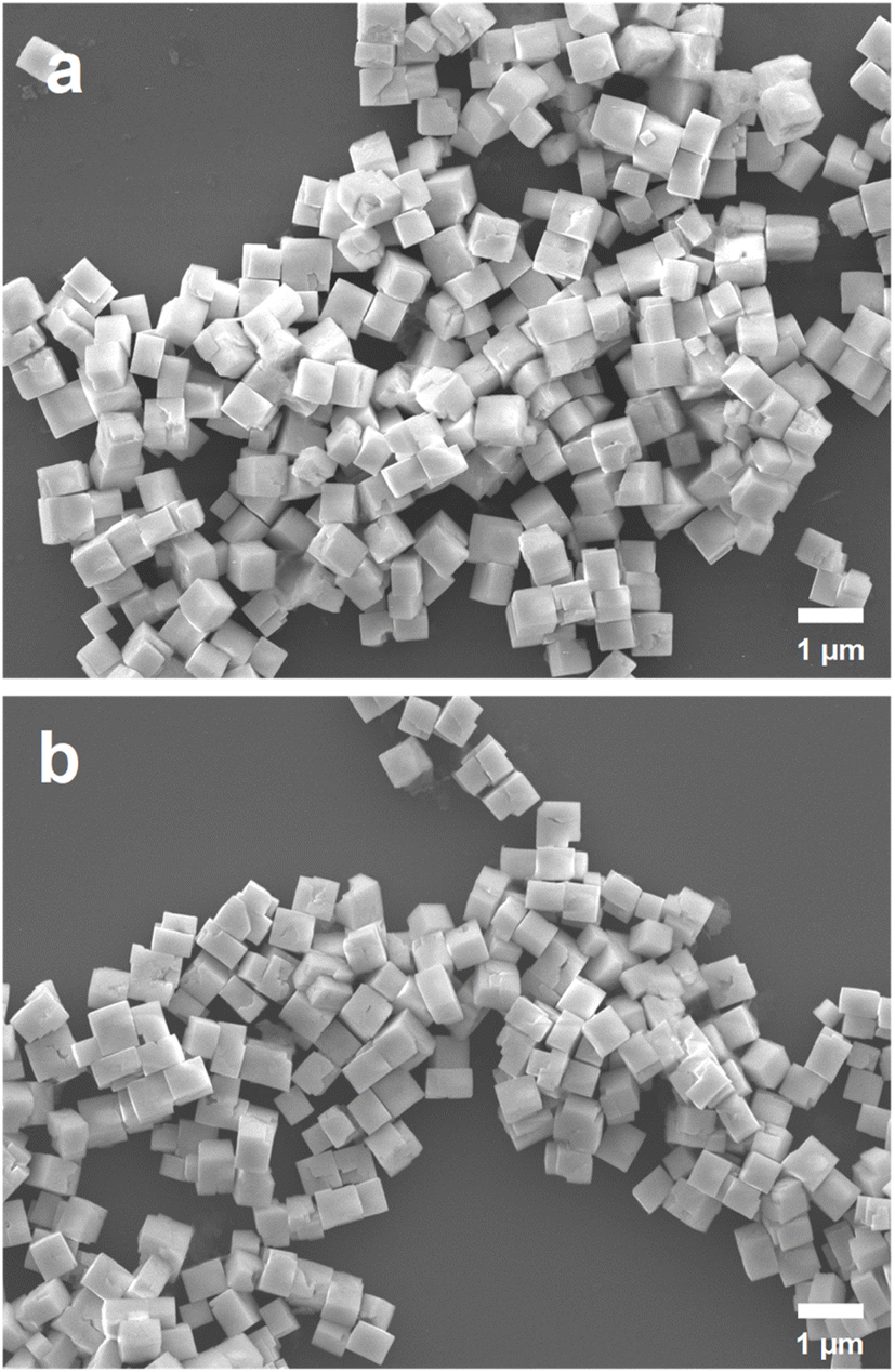 | ||
| Fig. 1 SEM images of the synthesized PbZr0.7Ti0.3O3 (a) cubes and (b) cuboids. | ||
Fig. 2 shows XRD patterns of the 555 nm PbZr0.7Ti0.3O3 cubes and 660 nm cuboids. XRD patterns of the size-tunable cubes are provided in Fig. S6 (ESI).† All the samples appear to match with a reference pattern of tetragonal phase PbZr0.52Ti0.48O3 (COD ID: 1521044) with a P4mm space group. No impurity peaks were detected. For the series of size-tunable cubes, the peak positions shift slightly to higher angles, indicating smaller lattice constants. Particle size-related lattice constant variation has been observed in MnS crystals.9 The XRD patterns show enhanced (001)/(100) peaks, as well as strong (002)/(200) peaks, suggesting the PbZrTiO3 crystals should expose {001} and {100} surfaces. The peak positions of cuboids also shift slightly to higher angles compared to cubes. The tiny XRD peak shifts are often not recognized, if the precise peak positions are not recorded. Fig. S7 (ESI)† shows XRD patterns of the PbZ0.6Ti0.4O3, PbZ0.55Ti0.45O3, and PbZ0.45Ti0.55O3 cubes. A reference pattern that more closely resembles these patterns is also shown. Significantly, for these samples, peaks with similar 2θ angles, such as the (001)/(100) peaks and (002)/(200) peaks, have become widely separated and easily identifiable. The peak separation should be due to a greater difference between unit cell constants a and c. There are also slight peak shifts with the perovskite composition.
 | ||
| Fig. 2 XRD patterns of the synthesized PbZr0.7Ti0.3O3 cubes and cuboids. A tetragonal phase pattern of PbZrTiO3 is also shown. | ||
To carefully analyze the interior lattices of the synthesized cubes and cuboids, a synchrotron X-ray wavelength of 0.43503 Å was used to obtain high resolution diffraction patterns (see Fig. S8, ESI†). The HR-XRD patterns were imported into GSAS Π software and refined with the P4mm space group. Unit cell constants were adjusted, and a zero-point shift correction was applied to ensure that the calculated peak positions match the observed ones. Various parameters such as microstrain, thermal vibration, and two-phase simulation were incorporated to better match the calculated peak profile with the observed peaks. Constraint equations were added to confine the fraction and position of atoms, aiming to stabilize the atomic thermal vibration. A two-phase simulation was conducted to better fit the asymmetric XRD peaks. The resulting simulation profiles are shown in Fig. 3. The simulation peaks are presented in gray, with the lighter gray representing the bulk phase and the darker gray representing the surface phase. The presence of two lattice phases indicates the existence of a surface layer in the PbZrTiO3 crystals. The refined cell parameters of PbZrTiO3 are detailed in Table S2, ESI.† All resulting refinement patterns meet the standard criteria for accuracy, as indicated by wR and R(F2). Microstrain is used to describe the degree of stretching experienced by lattices. Lattices in the crystal surface layer typically exhibit a higher microstrain, allowing for the distinction between surface and bulk phases. Table S2, ESI† reveals that the proportion of the surface layer in the PbZr0.7Ti0.3O3 cubes and cuboids is greater than that of the bulk. On the basis of bulk and surface layer fractions, the surface layer thicknesses are depicted in Fig. S9, ESI.† On the other hand, the bulk is the major lattice component for the three samples with different Zr to Ti atomic percentages. They also have larger c/a numbers.
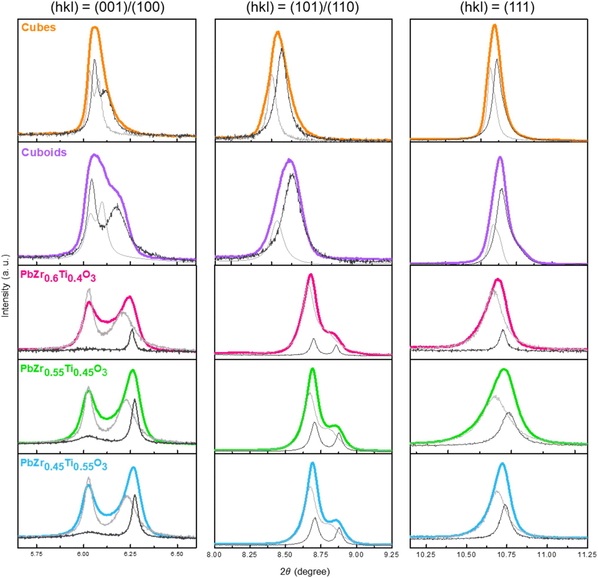 | ||
| Fig. 3 Expanded (001)/(100), (101)/(110), and (111) synchrotron XRD peaks of PbZr0.7Ti0.3O3 cubes and cuboids, and PbZr0.6Ti0.4O3, PbZr0.55Ti0.45O3, and PbZr0.45Ti0.55O3 cubes. The gray lines are outcomes of the two-phase simulation from the Rietveld refinement process. | ||
HR-TEM characterization of a single PbZr0.7Ti0.3O3 cube and cuboid is displayed in Fig. 4. The selected-area electron diffraction (SAED) patterns, obtained along the [010] zone axis, give discrete spots, implying their single crystallinity. However, streaks are only observed in the SAED pattern of the cuboid, suggesting lattice differences exist between the two samples. Through the fast Fourier transform process to convert a HR-TEM image to its diffraction pattern and reversing the diffraction pattern back to an image, a lattice spot image is obtained. Distinctly different lattice spot features can be identified for the cube and cuboid. Lattice fringes with d-spacings corresponding to the (110) and (100) planes of PbZrTiO3 were measured. On the basis of the TEM and XRD characterization, both samples should expose the same {100}, {010}, and {001} surfaces. However, the interior lattice features differ noticeably.
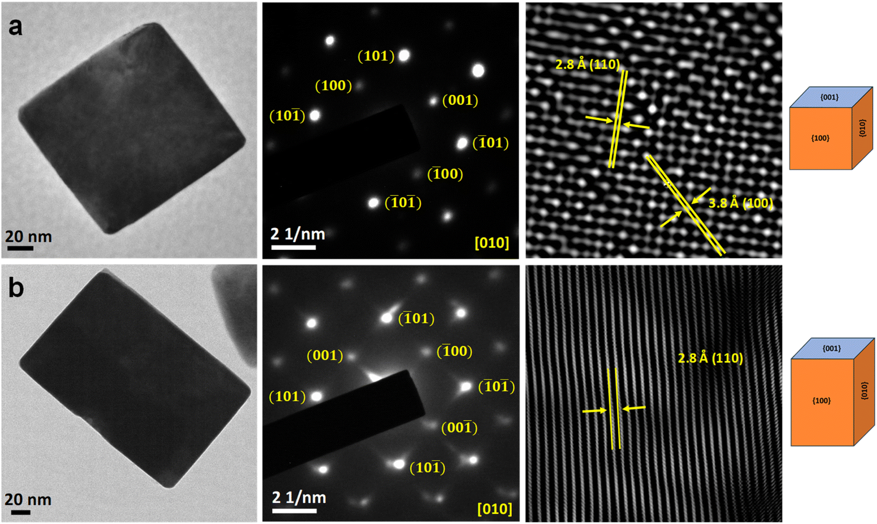 | ||
| Fig. 4 TEM images, SAED patterns, and FFT-derived lattice point images of (a) a PbZr0.7Ti0.3O3 cube and (b) a PbZr0.7Ti0.3O3 cuboid. The models show their exposed faces. | ||
The FFT-processed lattice point images provide visual evidence of the existence of the crystal surface layer region. Fig. 5c shows that the lattice points are elliptical dots in the crystal bulk of a cube, with dashes pointing toward certain directions. The streaks suggest that the atoms are slightly displaced due to the reaction temperature. Within ∼3 nm of the cube edge (Fig. 5f), each lattice spot appears to split into two parallel dashes. The separated dashes can merge together near the crystal surface. Also, the interior and surface dashes point along roughly perpendicular directions. These differences support the presence of bulk and surface layer lattices. For the cuboid bulk (Fig. 5i), slanted dashes running along two directions can be easily recognized. This lattice feature is clearly different from that of the cube and extends all the way to the cuboid surface, agreeing with the XRD refinement results of a greater surface layer fraction for cuboids (Fig. 5l). The streaks also become more elongated near the surface, indicating a larger degree of surface lattice deviation. The interior lattice differences between cubes and cuboids are also reflected in their dielectric constants (Fig. 6). At varying frequencies between 0 and 300 kHz, the dielectric constants of PbZr0.7Ti0.3O3 cuboids can be twice as large as those of cubes. This indicates their considerable lattice variations.
 | ||
| Fig. 5 (a, d, g and j) HR-TEM image of a portion of (a and d) a PbZr0.7Ti0.3O3 cube and (g and j) a cuboid. (b, e, h and k) The corresponding FFT-derived lattice point images of the red square areas. (c, f, i and l) Enlarged images of the white square areas. | ||
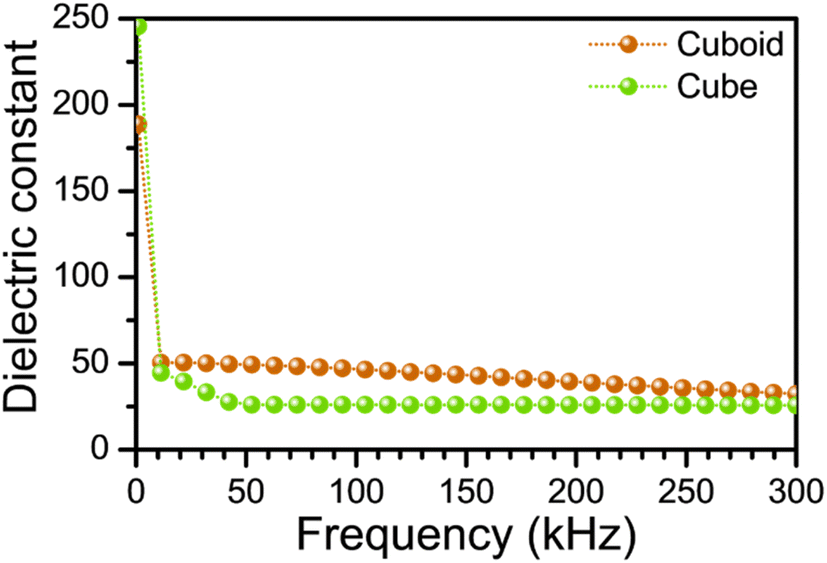 | ||
| Fig. 6 Frequency dependence of the dielectric constant of PbZr0.7Ti0.3O3 cubes and cuboids. | ||
Fig. 7 shows UV-vis diffuse reflectance spectra and the corresponding Tauc plots of all the synthesized PbZrTiO3 crystals. The absorption tail is red-shifted with increasing cube sizes. The band gaps of PbZr0.7Ti0.3O3 cubes measured at 538, 413, and 282 nm are 3.13, 3.18, and 3.22 eV, respectively. Despite their large dimensions, the band gap energy decreases continuously with increasing crystal sizes. This is the general observation for semiconductor crystals. The 555 nm PbZr0.7Ti0.3O3 cubes have a band gap of 3.19 eV, which is between those of the 282 and 413 nm cubes. An examination of their in-house XRD patterns shows that the 555 nm cubes have peak positions closer to the 282 nm cubes, and the peak positions deviate considerably from those of the 538 nm cubes. This result demonstrates that the interior lattice constant is also an important factor in light absorption. The cuboids have a band gap of 3.22 eV. With similar particle volumes to the 555 nm cubes, the shape-related optical effect should still be present due to their large lattice differences, although both samples expose the same crystal faces. PbZrTiO3 cubes with varying Zr:Ti atomic percentages also display band gap changes. The band gap increases slightly with a higher Zr ion percentage.
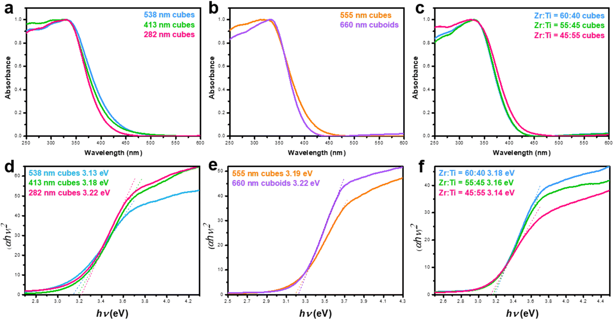 | ||
| Fig. 7 UV-vis diffuse reflectance spectra of (a) size-tunable PbZr0.7Ti0.3O3 cubes, (b) 555 nm PbZr0.7Ti0.3O3 cubes and 660 nm PbZr0.7Ti0.3O3 cuboids, and (c) PbZrxTi1−xO3 with different Zr:Ti atomic percentages. (d–f) Their corresponding Tauc plots. | ||
Piezoelectric and ferroelectric responses of all the PbZrTiO3 crystals were evaluated. Using piezoresponse force microscopy (PFM), the piezoresponse of a crystal, in terms of output voltage, was measured through tapping of a conductive atomic force microscopy (AFM) probe onto a particle, with an imposed swipe bias of −5 V to 5 V. Fig. S10 (ESI)† shows the AFM system. The amplitude–voltage butterfly loops of the crystals for piezoelectricity, generated from the spontaneous polarization, as well as phase–voltage hysteresis loops for ferroelectricity, were collected and are shown in Fig. 8 and S11 (ESI).† The cuboid achieved a maximum amplitude of 54–60 mV in this voltage range, while a cube from the 555 nm sample only delivered an amplitude of 22–30 mV. The three samples with tunable Zr:Ti atomic percentages have maximum amplitudes in the range of around 32–42 mV, so they have intermediate piezoelectric responses. The hysteresis loop arises from the reorientation of electric dipoles in response to an applied electric field, providing information about the ferroelectric performance of a material. The area enclosed by the hysteresis loop is largest for the cuboid and smallest for the PbZr0.7Ti0.3O3 cube. PbZr0.55Ti0.45O3 and PbZr0.6Ti0.4O3 cubes have an intermediate tip bias separation in their hysteresis loops. The greater lattice deviations in cuboids contribute to enhanced polarization and the alignment of electric dipoles, resulting in overall higher ferroelectric and piezoelectric responses.
 | ||
| Fig. 8 Amplitude–voltage butterfly loops of a single PbZr0.7Ti0.3O3 (a) cuboid and (b) cube. (c and d) The corresponding phase–voltage ferroelectric hysteresis loops. | ||
To further examine the piezoelectric output performance of PbZr0.7Ti0.3O3 cubes and cuboids, piezoelectric nanogenerator devices were constructed by mixing different weight percentages (10%, 20%, 30%, and 40%) of PbZrTiO3 powder with polydimethylsiloxane (PDMS) to determine the optimal composition, as shown in Fig. 9. The working principle of a PENG is based on the polarization of electric dipoles in the piezoelectric materials. Fig. S12 (ESI)† shows photographs of the fabricated PENG device for measurements of mechanical-to-electrical energy conversion. Fig. S13 (ESI)† illustrates the PENG mechanism under bending and releasing operation. When no external stimulus is applied, the piezoelectric material is electrically neutral with no piezoelectric signal or current flow. However, when an external stimulus like bending is applied, it causes deformation of the piezoelectric material's crystal structure. This structural change induces polarization of the electric dipoles, generating a piezoelectric potential field and consequently an electrical current flow in the external circuit. As the piezoelectric potential field diminishes, a current is induced in the opposite direction. The open-circuit voltages and short-circuit currents increase with the particle content from 10 to 30 wt%. However, the output signals drop with the content increasing to 40 wt%. Table S3 (ESI)† shows the output voltages and currents of the PENG devices. Lattice differences in PbZr0.7Ti0.3O3 cubes and cuboids should be linked to the output results, with cuboids exhibiting better performance at both open-circuit voltage and short-circuit current. The device containing 30 wt% PbZr0.7Ti0.3O3 cuboids exhibits the highest output signals, with an open-circuit voltage of 20.36 V and a short-circuit current of 2.30 μA. As seen in Table S4 (ESI),† both the cubes and cuboids exhibit generally stronger output signals than PENGs made using other reported PbZrTiO3 morphologies.
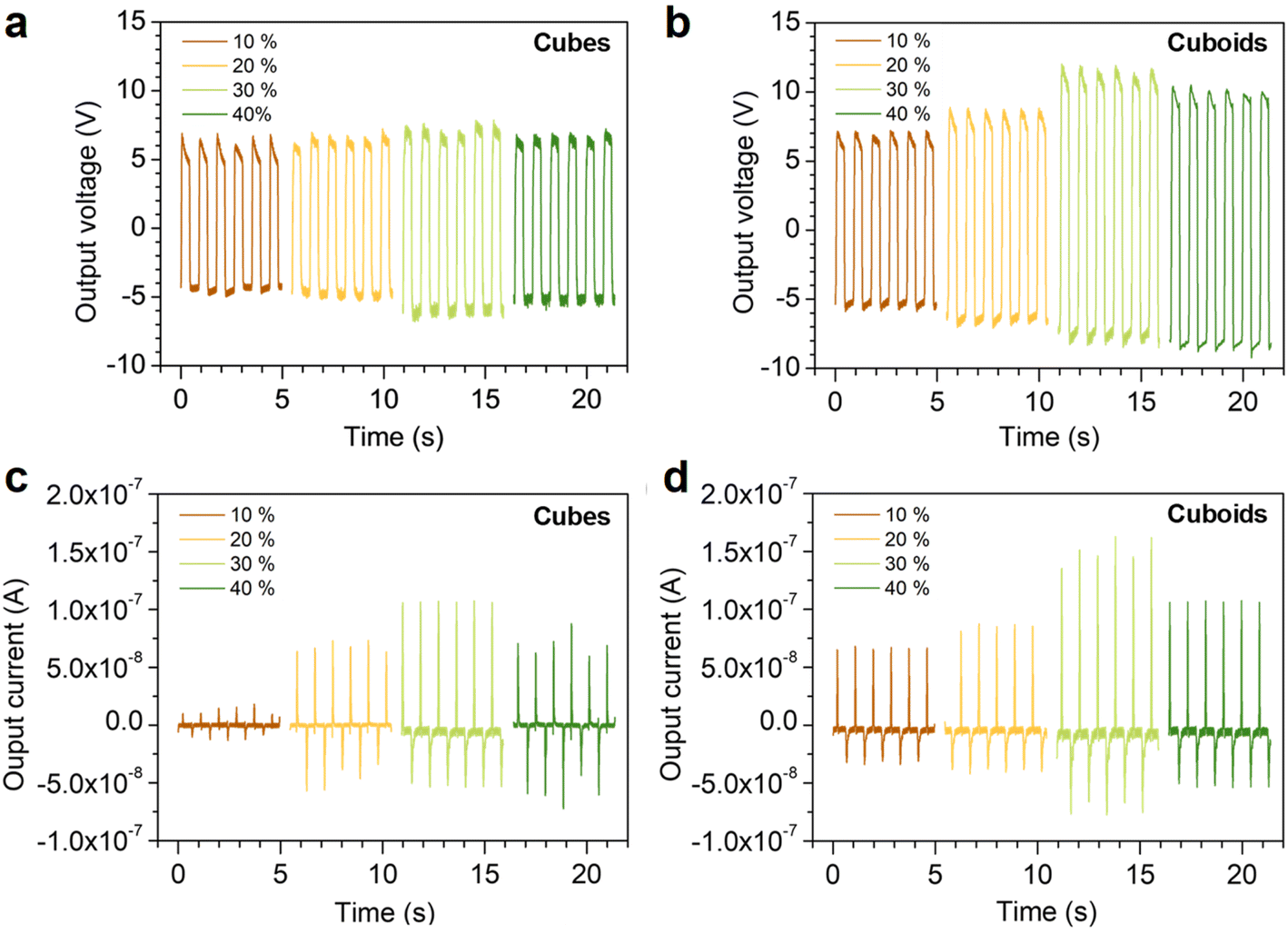 | ||
| Fig. 9 Electrical output performance characterization of the PENG. (a and b) Open-circuit voltages of PbZr0.7Ti0.3O3 cubes and cuboids with varying weight percentages. (c and d) Short-circuit currents of these PbZr0.7Ti0.3O3 cubes and cuboids. | ||
To determine the effective output power of the PENG device with 30 wt% cuboids, the connected load resistances were varied to measure the output signals (see Fig. S14, ESI†). The effective output power is the product of output current and output voltage. The maximum output power is 2.4 μW under a load resistance of 986 kΩ. To substantiate the energy harvesting capability of the fabricated PENGs, we have utilized the device under continuous bending and release cycles with a linear motor (Fig. S15a, ESI†). Before the energy harvesting application, switching polarity tests were performed to verify that the output signals originate from the piezoelectric response. The forward and reverse circuit connections of the device are depicted in Fig. S15b (ESI).† Under either circuit connection, the amplitudes of output voltage and current are similar but opposite in direction. For real-life applications, the fabricated PENG should provide a stable long-term output performance. Hence, the device was subjected to a long-term stability test at a frequency of 1 Hz (Fig. S16, ESI†). Very stable open-circuit voltage was recorded over 1500 s of bend–release cycles.
Furthermore, the devices containing 30 wt% crystals underwent electrical poling at ambient temperature by exposing them to a 5 kV electric field for 1 hour. While this poling process significantly enhanced the open circuit voltage outputs, the overall pattern of device response remained consistent with the unpoled samples, as demonstrated in Fig. S17, (ESI).† Besides, the humidity-dependent stability of a device was investigated, confirming the robustness of the PENG under different humidity conditions (Fig. S18, ESI†). The frequency-dependent performance of the same device was also examined. Fig. S19 (ESI)† shows that an increase in frequency will increase the output. However, as the average frequency of human motion is 1 Hz,27,28 this frequency is used for all the measurements. Moreover, Table S5 (ESI)† provides a comparison of the output performance of this device with other state-of-the-art PENGs based on different materials. PENGs incorporating the PbZrTiO3 cuboids give the best open-circuit voltage.29–33 However, the large substrate area (6 cm2) results in a lower current density.
The rectified output is utilized to charge a range of capacitors (0.1, 0.2, 0.3, 0.4, and 1.0 μF). The electrical circuit for the capacitor charging experiment and the results are shown in Fig. 10a–c. The harvested energy in the capacitor is then utilized to power a digital hygrometer and stopwatch (Fig. 10d–g). After the successful capacitor charging tests, the fabricated PENG was utilized to light commercial LEDs (Fig. 10h). Besides piezoelectric and ferroelectric behaviors, the PbZrTiO3 crystals should also possess pyroelectricity. Here, the PENGs were subjected to photothermal heating and cooling cycles by switching on and off an infrared lamp (PHILIPS, IR-175R-PAR, 175 W, 780–1400 mm in wavelength) every minute. A temperature difference of approximately 27 K can be achieved between the on and off states of the infrared lamp (Fig. 10i). Fig. 10 also shows the observed pyroelectric output voltages for the nanogenerators. Cuboids give higher pyroelectric output voltages than cubes.
 | ||
| Fig. 10 Capacitor charging experiments and energy harvesting demonstrations. (a) Schematic representation of the circuit connection for the capacitor charging by utilizing the PENG. (b) Charge output of the PENG with 30 wt% PbZrTiO3 cuboids. (c) Charging capability of the PENG under different capacitance capacities. (d and e) Powering a digital hygrometer. (f and g) Powering a digital stopwatch. (h) Powering two LEDs. (i) Cyclic changes in the temperature of the cuboid-based nanogenerator from infrared lamp irradiation cycles. (j and k) Pyroelectric responses of nanogenerators incorporating (j) cuboids and (k) cubes. | ||
The fabricated PENGs can also be utilized as self-powered motion detectors with very high precision. A single PENG device with 30 wt% cuboids was integrated with a shoe insole using double-sided adhesive tape. Various kinds of physical motions including walking, running, hopping, and squatting were performed by wearing that shoe, and the PENG can generate voltage outputs with different values and signal shapes (Fig. 11a). The accrued signal is then processed through the AutoML machine-learning model. The frequency and pressure of motion are also related to these output signals. Therefore, judging and recognizing exercise forms is possible by comparing the voltage peak value and frequency. A flowchart describing the method of motion detection using the machine learning-enhanced PENG is shown in Fig. 11b. The machine learning model's data analysis and classification procedures were applied to the collected sensing data. Herein, an integrated data collection system was utilized via wireless data transmission from the PENG to a computer (Fig. S20, ESI†). Using the machine learning model's predictive power, a confusion matrix is presented in Fig. 11c to support this result explicitly. The machine learning model achieves an accuracy of 96.8%. Hence, the device has potential applications in motion detection, physical abnormality detection, self-powered pressure sensing, and many more.
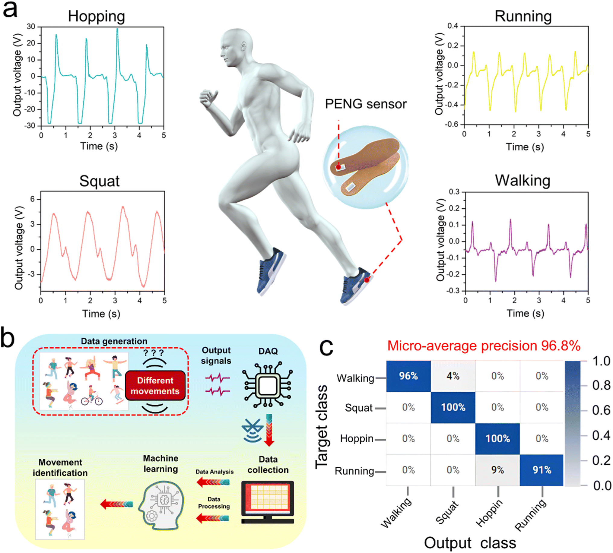 | ||
| Fig. 11 (a) Human motion detection using a single PENG sensor and the observed outputs for various movements. (b) Schematic representation of the flow diagram of the machine learning model for motion detection. (c) The confusion map of the machine-learning outcomes of human motion detection. | ||
Conclusions
PbZrTiO3 crystals with different sizes, shapes, and Zr:Ti atomic percentages have been hydrothermally synthesized. Synchrotron XRD analysis reveals the presence of bulk and surface layer lattices in all these samples. TEM characterization also shows lattice variations between the surface region and the inner bulk, and a PbZr0.7Ti0.3O3 cube and a cuboid have notably different lattice spot appearances even though they expose the same faces. Their dielectric constants also differ considerably. The crystals display size- and composition-dependent band gaps. A cuboid gives stronger piezoelectric and ferroelectric responses than a cube. A piezoelectric nanogenerator incorporating 30 wt% cuboids exhibits the highest open-circuit voltage of 20.36 V and short-circuit current of 2300 nA. The PENGs can harvest energy through bending/releasing cycles and photothermal heating/cooling. Remarkably, a single 30 wt% cuboid PENG device integrated into a shoe insole achieved an impressive 96.8% accuracy for human motion detection using a machine learning approach. Thus, crystal lattice variation through particle shape control can be a new way to enhance material properties. Future research could focus on developing environmentally friendly lead-free alternatives while maintaining comparable performance. Additionally, investigating the potential of different crystal morphologies beyond cubes and cuboids may provide even higher piezoelectric responses. The integration of these materials with flexible substrates and exploration of their applications in more complex wearable systems, such as full-body motion tracking or health monitoring devices, could expand their practical utility.
Experimental
Synthesis of PbZr0.7Ti0.3O3 cubes and cuboids
To grow PbZr0.7Ti0.3O3 cubes with tunable sizes, 100.3 μL of titanium bis(ammonium lactato)dihydroxide (TALH) solution was added to a vial containing 1 mL of water and stirred for 10 min. After the stirring period, 0.5 mL of 0.65 M ZrOCl2 solution was added into the titanium solution and stirred for 15 min. In another vial, 10 mL of 0.5 M KOH solution was added dropwise into a 1 mL solution containing 0.2898 g of Pb(NO3)2 and stirred for 25 min. Afterward, the two solutions were mixed together and stirred for 15 min. LiNO3 was not added in making 538 nm cubes, but was introduced to grow smaller cubes at the 10 min point of the 15 min stirring period. Next, the solution was transferred to a 30 mL Teflon-lined autoclave and heated at 200 °C for 2.5 h in an oven. The resulting white precipitate was collected by 11000 rpm centrifugation for 4 min, followed by sonicating with 4 mL of 10% acetic acid to remove unreacted lead oxide. Four more cycles of washing were carried out, including two times with 6 mL of deionized water, one time with a deionized water/ethanol mixture, and one time with 6 mL of ethanol. Finally, the particles were dispersed in 6 mL of ethanol for storage before characterization. The exact reagent amounts used are listed in Table S1 (ESI).† The same procedure was followed to grow 555 nm PbZr0.7Ti0.3O3 cubes and 660 nm cuboids. LiNO3 was not added. The reagent amounts used are also listed in Table S1 (ESI).†
Synthesis of PbZrTiO3 crystals with different Zr![[thin space (1/6-em)]](https://www.rsc.org/images/entities/h3_char_2009.gif) :Ti atomic percentages
:Ti atomic percentages
PbZrTiO3 crystals with different Zr:Ti atomic percentages were prepared using the same steps as those for making 413 nm PbZr0.7Ti0.3O3 cubes. By mainly tuning the relative amounts of TALH and ZrOCl2 solutions and adjusting the concentration and volume of KOH in making PbZr0.45Ti0.55O3 cubes, PbZr0.6Ti0.4O3 and PbZr0.55Ti0.45O3 cubes were also synthesized. Table S1 (ESI)† shows the reagent amounts used.
Piezoelectric nanogenerator fabrication
A 10:1 weight ratio of silicone elastomer base to silicone elastomer curing agent was added to a beaker. Next, PDMS and PbZrTiO3 nanocrystals were added and mixed by probe sonication with PbZrTiO3 contents of 10, 20, 30, and 40%. Subsequently, the solution was placed into a vacuum oven to degas. The PENG devices were fabricated by spin-coating the mixed solution of PDMS and PbZrTiO3 crystals onto an ITO/polyethylene terephthalate (PET) substrate (3 cm × 2 cm) at a spinning rate of 200 rpm for 30 s. Another piece of the ITO/PET substrate was then placed on the composite to construct a sandwich structure. Finally, the device was dried at room temperature for 30 h to allow the gel layer within the structure to solidify. Finally, copper wires were connected to the ITO electrodes for testing the nanogenerator device. A flowchart of the PENG fabrication process is shown in Fig. S21 (ESI).†
Instrumentation
XRD patterns were obtained using a Bruker D2 PHASER diffractometer operating at 30 kV and 10 mA with Cu Kα radiation. Synchrotron XRD patterns were collected at the Taiwan Photon Source 19A (TPS 19A) high resolution powder X-ray diffraction beamline with an X-ray energy of 28.5 keV. SEM images were taken with the use of a JEOL JSM-7000F electron microscope. TEM characterization was performed on a JEOL JEM-F200 electron microscope. UV-vis diffuse reflectance spectra were collected by using a JASCO V-770 spectrophotometer with a solid sample holder. Using a Pt/Ir-coated silicon-based conductive AFM tip (OSCM-PIT), piezoelectric responses and hysteresis loops were obtained by piezoresponse force microscopy (PFM) using a Bruker Dimension Icon atomic force microscope that was enabled with ScanAsyst.34 Measurements of output voltage and current were made with a high resistance Keithley 6517B electrometer. An extremely accurate LCR meter (LCR-6300, GW Instek) was used to measure the dielectric constants. A TENMARS TM 747 4-channel thermometer was used to detect the temperature. A CHI 6025E electrochemical analyzer was used to measure the pyroelectric output voltage.Data availability
All the data have been presented in the manuscript and ESI.†Author contributions
Y.-J. C. and A. P. contributed equally to this work. Y.-J. C. synthesized and characterized the crystals. A. P. fabricated the nanogenerators, tested their ferroelectric and piezoelectric responses, performed the machine learning study, and helped in the review process. B.-H. C. collected and analyzed the synchrotron XRD patterns. S. J. collected the TEM images. S. S. conducted pyroelectric measurements and helped in the motion detection study. Z.-H. L. and M. H. H. supervised the project. M. H. H. wrote the manuscript.Conflicts of interest
There are no conflicts to declare.Acknowledgements
The funding for this research was provided by the National Science and Technology Council, Taiwan (NSTC 112-2113-M-007-016-MY3 and 113-2628-E-002-010-MY3).References
- A.-T. Lee, C.-S. Tan and M. H. Huang, ACS Cent. Sci., 2021, 7, 1929–1937 CrossRef CAS.
- G. Kumar, C.-R. Chen, B.-H. Chen, J.-W. Chen and M. H. Huang, J. Mater. Chem. C, 2022, 10, 12125–12131 RSC.
- C.-S. Tan, H.-S. Chen, C.-Y. Chiu, S.-Z. Wu, L.-J. Chen and M. H. Huang, Chem. Mater., 2016, 28, 1574–1580 CrossRef CAS.
- G. Kumar, Z.-L. Chen, S. Jena and M. H. Huang, J. Mater. Chem. C, 2023, 11, 3885–3888 RSC.
- Z.-L. Chen and M. H. Huang, J. Mater. Chem. A, 2023, 11, 22198–22205 RSC.
- H.-H. Ma and M. H. Huang, J. Mater. Chem. C, 2023, 11, 5857–5866 RSC.
- Y.-C. Yang, Y.-W. Peng, A.-T. Lee, G. Kumar and M. H. Huang, Inorg. Chem. Front., 2021, 8, 4685–4695 RSC.
- P.-S. Chang, B.-H. Chen, Y.-C. Lin, W.-T. Dai, G. Kumar, Y.-G. Lin and M. H. Huang, Small, 2024, 20, 2401558 CrossRef CAS.
- C.-K. Chen, B.-H. Chen and M. H. Huang, Chem. Mater., 2023, 35, 7859–7866 CrossRef CAS.
- G. Kumar, H.-W. Sun and M. H. Huang, ACS Appl. Nano Mater., 2024, 7, 2155–2163 CrossRef CAS.
- J.-W. Chen, A. Pal, B.-H. Chen, G. Kumar, S. Chatterjee, K. Peringeth, Z.-H. Lin and M. H. Huang, Small, 2023, 19, 2205920 CrossRef CAS.
- B.-H. Chen, G. Kumar, Y.-J. Wei, H.-H. Ma, J.-C. Kao, P.-J. Chou, Y.-C. Chuang, I.-C. Chen, J.-P. Chou, Y.-C. Lo and M. H. Huang, Small, 2023, 19, 2303491 CrossRef CAS.
- S. Thoka, A.-T. Lee and M. H. Huang, ACS Sustainable Chem. Eng., 2019, 7, 10467–10476 CrossRef CAS.
- S. Zhang, X. Lin, H. Liu, Z. Yuan, Y. Huan, X. Yuan, S. Huang and X. Cheng, Int. J. Energy Res., 2020, 45, 6213–6226 CrossRef.
- C. Ren, G. Zhong, Q. Xiao, C. Tan, M. Feng, X. Zhong, F. An, J. Wang, M. Zi and M. Tang, Adv. Funct. Mater., 2020, 30, 1906131 CrossRef CAS.
- M. M. Kržmanc, Z. Kutnjak and M. Spreitzer, Crystals, 2022, 12, 1514 CrossRef.
- Y. Takada, K. Mimura and K. Kato, J. Ceram. Soc. Jpn., 2018, 126, 326–330 CrossRef CAS.
- S.-B. Cho, M. Oledzka and R. E. Riman, J. Cryst. Growth, 2001, 226, 313–326 CrossRef CAS.
- S. W. Ma, Y. J. Fan, H. Y. Li, L. Su, Z. L. Wang and G. Zhu, ACS Appl. Mater. Interfaces, 2018, 10, 33105–33111 CrossRef CAS.
- W. S. Jung, M. J. Lee, S. J. Yoon, W. H. Lee, B. K. Ju and C. Y. Kang, Int. J. Appl. Ceram., 2015, 13, 480–486 CrossRef.
- D. Zou, S. Liu, C. Zhang, Y. Hong, G. Zhang and Z. Yang, Nano Energy, 2021, 85, 105984 CrossRef CAS.
- Y. Zhang, W. Zhu, C. K. Jeong, H. Sun, G. Yang, W. Chen and Q. Wang, RSC Adv., 2017, 7, 32502–32507 Search PubMed.
- W. Tang, Q. Sun and Z. L. Wang, Chem. Rev., 2023, 123, 12105–12134 CrossRef CAS.
- X. Chen, J. Li, Y. Liu, J. Jiang, C. Zhao, C. Zhao, E. G. Lim, X. Sun and Z. Wen, ACS Appl. Mater. Interfaces, 2021, 13, 61789–61798 Search PubMed.
- Z. Huo, Y. Wei, Y. Wang, Z. L. Wang and Q. Sun, Adv. Funct. Mater., 2022, 32, 2206900 CrossRef CAS.
- K. Dong, X. Peng, R. Cheng, C. Ning, Y. Jiang, Y. Zhang and Z. L. Wang, Adv. Mater., 2022, 34, 2109355 CrossRef CAS.
- H. Xiang, X. Li, B. Wu, S. Sun and P. Wu, Adv. Mater., 2023, 35, 2209581 CrossRef CAS.
- X. Guo, T. He, Z. Zhang, A. Luo, F. Wang, E. J. Ng, Y. Zhu, H. Liu and C. Lee, ACS Nano, 2021, 15, 19054–19069 CrossRef.
- S. Xu, Y. Yeh, G. Poirier, M. C. McAlpine, R. A. Register and N. Yao, Nano Lett., 2013, 13, 2393–2398 CrossRef PubMed.
- K. Y. Lee, D. Kim, J. H. Lee, T. Y. Kim, M. K. Gupta and S. W. Kim, Adv. Funct. Mater., 2014, 24, 37–43 CrossRef.
- B. K. Yun, Y. K. Park, M. Lee, N. Lee, W. Jo, S. Lee and J. H. Jung, Nanoscale Res. Lett., 2014, 9, 4–7 CrossRef PubMed.
- J. H. Jung, M. Lee, J. I. Hong, Y. Ding, C. Y. Chen, L. J. Chou and Z. L. Wang, ACS Nano, 2011, 5, 10041–10046 CrossRef PubMed.
- R. Ding, H. Liu, X. Zhang, J. Xiao, R. Kishor, H. Sun, B. Zhu, G. Chen, F. Gao, X. Feng, J. Chen, X. Chen, X. Sun and Y. Zheng, Adv. Funct. Mater., 2016, 26, 7708–7716 CrossRef.
- A. Pal, A. Ganguly, P.-H. Wei, S. R. Barman, C.-C. Chang and Z.-H. Lin, Adv. Sci., 2024, 11, 2307266 CrossRef PubMed.
Footnotes |
| † Electronic supplementary information (ESI) available. See DOI: https://doi.org/10.1039/d4sc06643j |
| ‡ These authors contributed equally: Ya-Ju Chuang and Arnab Pal. |
| This journal is © The Royal Society of Chemistry 2025 |