
 Open Access Article
 This Open Access Article is licensed under a Creative Commons Attribution-Non Commercial 3.0 Unported Licence
Dual back interface engineering optimized charge carrier dynamics in Sb2(S,Se)3 photocathodes for efficient solar hydrogen production†
Hafiz Sartaj
Aziz
 a,
Tahir
Imran
a,
Munir
Ahmad
a,
Guo-Jie
Chen
a,
Ping
Luo
a,
Dong-Lou
Ren
b,
Bing-Suo
Zou
b,
Ju-Guang
Hu
a,
Zheng-Hua
Su
a,
Pei-Guang
Yan
a,
Guang-Xing
Liang
a and
Shuo
Chen
*a
a,
Tahir
Imran
a,
Munir
Ahmad
a,
Guo-Jie
Chen
a,
Ping
Luo
a,
Dong-Lou
Ren
b,
Bing-Suo
Zou
b,
Ju-Guang
Hu
a,
Zheng-Hua
Su
a,
Pei-Guang
Yan
a,
Guang-Xing
Liang
a and
Shuo
Chen
*a
aShenzhen Key Laboratory of Advanced Thin Films and Applications, Key Laboratory of Optoelectronic Devices and Systems of Ministry of Education and Guangdong Province, State Key Laboratory of Radio Frequency Heterogeneous Integration, College of Physics and Optoelectronic Engineering, Shenzhen University, Shenzhen 518060, China. E-mail: chensh@szu.edu.cn
bState Key Laboratory of Featured Metal Materials and Life-cycle Safety for Composite Structures, Guangxi Key Laboratory of Processing for Non-ferrous Metals and Featured Materials, School of Resources, Environment and Materials, Guangxi University, Nanning, Guangxi 530004, China
First published on 2nd December 2024
Abstract
Antimony sulfoselenide (Sb2(S,Se)3) is a promising sunlight absorber material for solar energy conversion in photovoltaic (PV) cells and photoelectrochemical (PEC) photoelectrodes due to its excellent photoelectric properties. However, the obtained thin-film and back contact properties significantly influence the PEC performance of photocathodes, causing severe bulk recombination, carrier transport loss, and deteriorating half-cell solar-to-hydrogen (HC-STH) efficiency. This study introduces an intriguing dual back interface engineering strategy for Sb2(S,Se)3 photocathodes by incorporating an intermediate MoO2 layer and a secondary carrier transport channel of Au to strengthen charge carrier dynamics. The synergistic assembly of these dual back interface layers improves the growth kinetics and achieves the optimal orientation of Sb2(S,Se)3 thin films by increasing substrate wettability. Moreover, by shortening the back contact barrier height and passivating defect-assisted recombinations, these dual back underlayers simultaneously enhance carrier transport and separation efficiencies. As a result, the photocurrent density of the champion Sb2(S,Se)3 photocathode increases from 5.89 to 32.60 mA cm−2, and the HC-STH conversion efficiency improves significantly from 0.30% to 3.58%, representing the highest value for Sb2(S,Se)3-based photocathodes. This work highlights the effectiveness of dual back interface engineering in promoting the PEC performance of chalcogenide photocathodes for solar hydrogen evolution applications.
1. Introduction
Recent advancements in photoelectrochemical (PEC) characteristics have explored various semiconductor materials, including silicon, metal oxides, metal sulfides, metal tellurides, and organic–inorganic perovskites.1–8 Among these, Sb2(S,Se)3 is a popular absorber because of its low toxicity, high absorption coefficient with a tunable bandgap, benign hole mobility, and superior stability.9–11 Despite ongoing efforts to improve its film quality and power conversion efficiencies in PV and PEC cells, Sb2(S,Se)3 photoelectric devices still fall short of their superior counterparts.12–14 This significant performance deficit is primarily associated with the complex defect chemistry, leading to severe charge carrier recombination.9 Thus, a comprehensive understanding and optimization of Sb2(S,Se)3 device efficiency is indispensable.Synthesizing high-quality absorber films with a compact, smooth morphology, devoid of secondary phases and defects, is a prerequisite for optimal performance in photoelectric applications. However, synthesis challenges of the Sb2(S,Se)3 absorber stem from its low-symmetry crystal structure and intricate bulk defect characteristics.11 Particularly, defects at bulk and deep levels are considered detrimental, significantly deteriorating performance by trapping charge carriers and decreasing carrier extraction efficiency.15–17 Several fabrication approaches for chalcogenide materials (i.e., Sb2(S,Se)3 and Sb2Se3 thin films), including the successive low-temperature pulsed electron deposition technique (LT-PED), magnetron sputtering deposition (MSD), vapour transport deposition (VTD), using molecular ink, spin coating, electrodeposition, chemical bath deposition (CBD), and hydrothermal deposition (HD), have resulted in 7–10% PV cell efficiencies.10,17–21 Notably, the HD process is particularly effective in producing compact and homogeneous Sb2(S,Se)3 films owing to its low processing temperature, which impedes interfacial element diffusion and additional defects.19,20 Furthermore, the HD approach involves reactive ion deposition in aqueous solutions, followed by nucleation and crystal growth processes.22
In 2017, Moon et al. first investigated a pure Sb2Se3 photocathode for PEC water splitting,23 which sparked a range of subsequent studies on this intriguing scenario in areas like co-catalyst engineering, absorber engineering, interface engineering, and tandem engineering.2,7,24–27 Despite these advances, current research predominantly focuses on pure Sb2Se3 absorbers, with limited research on Sb2(S,Se)3 alloy-type photocathodes, which are isomorphous and share identical unit-cell parameters.28–32 The Sb2(S,Se)3 and Sb2S3 films grown via the hydrothermal method provide a better (hk1) orientation, preventing lattice mismatch and deep-level defects due to in situ substitution of S and Se.28,29 Furthermore, a gradient S concentration nurtures charge carrier transport and separation, and extends the band-bending region.30 Recently, the Sb2(S,Se)3 photocathode fabricated through the VTD method achieved a photocurrent density (Jph) of 16.5 mA cm−2 and an STH efficiency of 1.1%.17 However, the performance of the Sb2(S,Se)3 photocathode is far inferior compared to its Sb2Se3 counterpart, which has already obtained a benchmark Jph value above 30 mA cm−2.2,8,33 Therefore, optimizing back interface engineering is essential for improving thin film quality and PEC performance of Sb2(S,Se)3 photocathodes.
To date, most studies have focused on preparing Sb2(S,Se)3 devices with superstrate structures due to simplicity and ohmic contacts. However, substrate configurations offer significant advantages like direct sunlight absorption, enhanced interface quality, and a customizable absorber layer.34 Unfortunately, insufficient research exists related to Sb2(S,Se)3 devices with a substrate structure, which exhibits potential advantages for photocathodes. Back interface engineering is significantly important for enhancing performance efficiencies, such as Jph, onset potential (Von), and HC-STH.35–37 Effective carrier transport and extraction rely on optimizing the back interface, which involves reducing the back contact barrier height and the absorber layer's development mechanisms.36,37 On the other hand, post-annealing can improve substrate wettability by reducing the contact angle and enhancing interfacial bonding strength.38 Besides, it increases surface energy and adhesion, improving compatibility with the substrate and buffer layers.39,40 To encourage charge transport, the incorporation of the carrier transport channel as an underlayer (interfacial layer) considerably influences carrier dynamics at the interface. Atomic-level interactions between adjacent components form numerous chemical bonds in heterojunctions, which facilitate efficient carrier transport and separation, such as Au–O bonds at the Au–MoO2 interface acting as an electronic-transmission medium for promoting the hydrogen evolution reaction (HER).41,42 The study on the modification of wettability, charge carrier dynamics, and back contact barrier height at the Mo/Sb2(S,Se)3 interface is under-researched, requiring further examination for improvement and potential advancement in PEC.
This study explores a dual back interface engineering approach for optimizing charge carrier dynamics in planar-type Mo/MoO2/Au/Sb2(S,Se)3/CdS/TiO2/Pt photocathodes. The synergy of dual back interface (an intermediate layer of MoO2 followed by a secondary carrier transport channel of Au) layers strengthens the growth kinetics by acquiring the ideal orientation of the Sb2(S,Se)3 film through better substrate wettability. Moreover, this approach shortens the back contact barrier height and suppresses defect-assisted recombination, leading to simultaneously enhanced charge carrier transport and separation efficiencies. Under this engineering effort, the champion photocathode offers advantageous perceptions of regulating the bulk and interface properties, leading to a remarkable Jph of ∼32.60 mA cm−2 (at 0 V versus the reversible hydrogen electrode (RHE), i.e., VRHE). An HC-STH conversion efficiency of ∼3.58% undoubtedly strengthens its potential for applications in solar hydrogen production.
2. Experimental section
2.1. Preparation of the Mo substrate
This study describes the use of the hydrothermal method to deposit an Sb2(S,Se)3 film onto Mo-coated soda lime glass (SLG) substrates. Initially, the deposition was very weak and inhomogeneous (Fig. S1a and b†). To address this issue, post-annealing was used to enhance the substrate's wettability. The Mo substrates were ultrasonically washed with deionized water, detergent, and ethanol, and then transferred to a furnace. Before moving the Mo substrates, the furnace tube was thoroughly cleaned with detergent and distilled water. As the furnace temperature reached 100 °C, the furnace tube was vacuumed and cleaned three times with argon, and then filled with a predetermined volume of air, and tightened from both ends. The Mo substrates were annealed at various temperatures (200 °C, 300 °C, 400 °C, and 500 °C) for 15 minutes to produce a MoO2 interface layer. After annealing, three types of Mo substrates were selected for further processing: unannealed, post-annealed at 400 °C, and post-annealed at 400 °C followed by Au sputtering.2.2. Preparation of Sb2(S,Se)3 thin films
The as-prepared Mo substrates were subjected to deposition of the thin films of Sb2(S,Se)3via the hydrothermal method. To prepare the precursor solution, 0.025 g of SeC(NH2)2, 0.267 g of K2Sb2(C4H2O6)2·3H2O, and 0.794 g of Na2S2O3·5H2O were dissolved in 40 mL of deionized water and stirred to form a homogeneous yellow solution. This solution was added to a Teflon container, with Mo substrates angled appropriately opposite to the wall. The hydrothermal reaction was conducted at 135 °C for 5 h. Afterward, the samples were cleaned with deionized water and ethanol, and then dried with compressed nitrogen. Finally, the films were selenized at 410 °C for 15 minutes using 0.4 g of high-purity Se powder in a tube furnace.342.3. Preparation of the Sb2(S,Se)3 photocathode
The buffer layer (CdS) was produced using the CBD method, while the TiO2 protective layer was deposited using an atomic layer deposition (ALD) technique, according to previous research.2 Afterwards, Pt was sputtered on the top side as a co-catalyst for 50 seconds at a current of 20 mA using a 108 Auto Sputter Coater. Prior to performance testing, Ag colloids were coated over the exposed surface of the Mo substrate to establish metal contact. A detailed schematic of the preparation procedure is illustrated in Fig. S2.†2.4. Characterization
The phase and crystal structure of the Sb2(S,Se)3 thin films were examined by using an X-ray diffractometer using CuKα radiation (XRD, Ultima-iv). The cross-section and surface morphologies of the films were observed by scanning electron microscopy (SEM, Zeiss SUPRA 55), and the corresponding chemical compositions were analyzed with an energy dispersive spectroscope (EDS, BRUKER QUANTAX 200). The states of the film surface were investigated by X-ray photoelectron spectroscopy (XPS, ESCALAB 250Xi). A contact angle meter was employed to measure contact angles at ambient temperature (PERFECT WAM-100). The thin film surface roughness and morphologies were investigated by using an atomic force microscope (AFM) operated via NT-MDT Spectrum Instruments in semi-contact mode. For analyzing the bonding information, Raman spectroscopy was employed (Renishaw, InVia). Topography and surface potential characterization studies of Sb2(S,Se)3 films were performed through a Kelvin probe force microscope (KPFM, Bruker Dimension ICON). The Sb2(S,Se)3 film's absorption and reflection spectra were obtained through a Shimadzu UV-3600 spectrophotometer. PEC measurements were carried out by using a CHI660e electrochemical workstation. The characterization was carried out in a 0.5 M H2SO4 electrolyte with 100 mW cm−2 AM 1.5G simulated solar illumination, and the details are provided in Note S1.† A PHI 5000 VersaProbe was used to conduct ultra-violet photoelectron spectroscopy (UPS) coupled with a He I source at 21.22 eV. Under simulated sunlight illumination, photoelectrochemical impedance spectroscopy (PEIS) was performed. To determine the flat-band potential (Efb) of the Sb2(S,Se)3 films, Mott–Schottky (M–V) characterization studies were performed in the dark using a 30 mV AC amplitude plus a frequency of 104 Hz and a scanning voltage between −0.50 and 0.10 V. The temperature-dependent dark J–V (J–V–T) characterization studies were carried out by utilizing a Keithley 4200A-SCS system coupled with a Lakeshore 325 temperature controller. Capacitance–voltage (C–V) measurements were carried out at a 30 mV AC amplitude, 104 Hz frequency, and a voltage range of −0.50 to 0.10 V in the dark. Drive-level capacitance profiling (DLCP) was performed using AC amplitudes of 20–140 mV and DC voltages of −0.25 to 0 V. Admittance spectroscopy of the devices was performed in a Janis VPF (Lake Shore, 325 Cryogenic Temperature Controller) –100 cryostat with the frequency range of 102–106 Hz and the temperature range of 340–110 K.3. Results and discussion
3.1. Dual back interface engineering for optimized growth kinetics of Sb2(S,Se)3 films
Wettability is determined by using the contact angle (CA) between the fluid and solid surface and can be categorized as completely wettable (CA = 0°), hydrophilic (CA < 90°), or hydrophobic (CA > 90°).39 For Sb2(S,Se)3 thin films on Mo substrates, the CA was measured with water droplets. The CA produced by dropping a deionised water droplet depends mainly on the roughness and surface energies of the interfaces between the solid and liquid surfaces.7Fig. 1a–c display pristine Mo (unannealed), post-annealed Mo (at 400 °C/15 min), and post-annealed Mo (at 400 °C/15 min) sputtered with Au, corresponding to CAs 44.2°, 19.8°, and 31.7°, respectively. For comparison, the CAs (37.3°, 14.7°, and 21.9°, respectively) of the identical samples were also measured with glycerol droplets which showed similar tendencies (Fig. S3a–c†). Besides, post-annealing at lower temperatures (200 °C and 300 °C) resulted in CAs of 20.5° and 17.9°, respectively (Fig. S4a and b†). Typically, the CA decreases as post-annealing temperature increases, because the annealing process increases the surface energy of thin films, which improves wettability by reducing the CA and strengthening the interfacial bonding.38,40 Consequently, Mo substrates show better wettability at annealing temperatures up to 400 °C/15 min, enabling high-quality Sb2(S,Se)3 film deposition. However, annealing at 500 °C/15 min weakened the adhesion between the glass and Mo, causing the thin film to peel off after gradual washing with deionized water (Fig. S4c†). This could explain the deformation or distortion observed as a result of the high-temperature annealing process.38 | ||
| Fig. 1 (a–c) The measured CAs (using water droplets) of pristine Mo, post-annealed Mo at 400 °C/15 min, and post-annealed Mo sputtered with Au, respectively. (d–f) The measured CAs of the thin films from HS1, HS2, and HS3 samples and (g–i) the corresponding AFM topographical images of the thin films from HS1, HS2 and HS3 samples. | ||
After the HD of the Sb2(S,Se)3 absorber on three distinct Mo substrates, pristine Mo (unannealed), post-annealed Mo (at 400 °C/15 min), and post-annealed Mo sputtered with Au were chosen for further analysis, and they were named HS1, HS2, and HS3, respectively. According to Fig. 1d and e, the HS1 and HS2 thin-film surfaces exhibit inferior hydrophilic behaviour with CAs of 87.9° and 73.3°, respectively. The CA of the HS3 film is 61.6° (Fig. 1f), which indicates a superior hydrophilic nature, suggesting an obvious improvement in wettability. The glycerol droplet measurements for the identical samples showed similar CAs tendency: 85.5°, 71.0°, and 59.1° (Fig. S3d–f†). The changes in CA values are attributed to differences in chemical composition, grain size, roughness, and surface energy of the Sb2(S,Se)3 films. However, improved wettability can enhance PEC performance by increasing exposed reaction sites and facilitating photoelectron transfer, thus triggering the HER.7 Moreover, the effects of introducing the MoO2 oxide layer and the subsequent insertion of carrier transport channel Au on the associated surface morphologies, wettability, and roughness of the corresponding HS1, HS2, and HS3 thin films were examined using AFM measurements. Fig. 1g and h show crystal grain profiles for HS1, with an average root-mean-square (RMS) surface roughness of 41.5 nm and 57.4 nm for the HS2 thin film surface. However, Wenzel's roughness-dependent wettability model suggests that roughness will increase the hydrophilicity of a naturally hydrophilic surface (CA < 90°).39 Thus, a higher RMS roughness value of 77.2 nm as shown in Fig. 1i (Table S1†), which is ≈60% rougher than HS1, increases the wettability of the Mo/MoO2/Au/Sb2(S,Se)3 film (HS3). Generally speaking, variations in the CA and roughness are caused by the formation of the MoO2 oxide layer resulting from the post-annealing process and the insertion of the carrier transport channel Au layer.
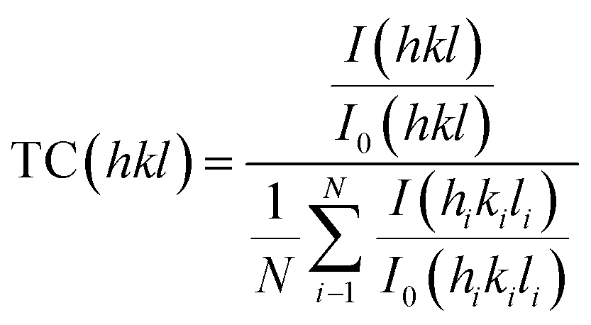
The XRD measurements were conducted to investigate how post-annealing influences the Mo substrate and Sb2(S,Se)3 thin-film crystalline structures to assess variations in device performance. Fig. 2a shows the development of a thin and smooth MoO2 intermediate layer in the form of crystal phases (JCPDS#32-0671) on the Mo substrate surface, where pristine Mo represents an unannealed substrate, and post-annealed Mo denotes the annealed (at 400 °C/15 min) substrate. The XRD data stipulate that the formation of the MoO2 intermediate layer on the Mo substrate surface resulted in a decreased contact angle and enhanced bonding strength by increasing surface energy.43 To further confirm the existence of the MoO2 oxide layer, the identical specimens' surface and cross-sectional morphologies were investigated via SEM (Fig. S5a–f†). It is evident that the annealed sample's surface got rougher compared to pristine Mo (Fig. S5a and b†), and it has a compact and smooth layer of MoO2 (Fig. S5e†). Furthermore, a combined thin layer of the intermediate layer MoO2 and the charge transport channel Au is also observed (Fig. S5f†). Besides, the XRD data of the HS1, HS2, and HS3 films are demonstrated in Fig. 2b. All the peaks of HS1, HS2, and HS3 thin films match well with JCPDS (No. 15-0861 for Sb2Se3) and (No. 42-1393 for Sb2S3) having no secondary phases. The presence of S in the samples is shown by the dot-filled dark yellow lines (Fig. 2b). Additionally, there is an improvement in crystallinity and an effective suppression of random orientations. The preferred orientations corresponding to the (211), (221), and (002) planes of Sb2(S,Se)3 peaks are observed in the HS2 and HS3 films, which are expected to influence the performance diversity of the photocathodes. Compared with HS1, the (020), (120), and (130) orientations of the HS3 film decreased, while the (211) and (221) orientations progressively increased. Such growth in the (211) and (221) oriented peaks of Sb2(S,Se)3 is connected to the synergetic effect of MoO2 and Au dual back underlayers on inhibiting the hopping-type transport based on (hk0).44 The results were further confirmed by analyzing the TC (texture coefficient) to examine the preferred orientation peaks in Sb2(S,Se)3 thin films, and the following equation can be used to calculate the TC:34,37
 | (1) |
 | ||
| Fig. 2 (a) XRD patterns of pristine and post-annealed (400 °C/15 min) Mo substrates. (b) XRD patterns, (c) texture coefficients, and (d–f) XPS peaks of thin films from HS1, HS2 and HS3 samples. (g–i) SEM images of the surface morphology, and (j–l) cross-sectional SEM images of thin films from HS1, HS2 and HS3 samples. | ||
The total XPS spectra were recorded from HS1, HS2, and HS3 films (Fig. S7†) to analyze the elemental composition of Sb2(S,Se)3 thin films. The XPS spectra of the three primary elements (Sb 3d, S 2p, and Se 3d) in Sb2(S,Se)3 films are illustrated in Fig. 2d–f. The two prominent peaks at 538.7 and 529.5 eV are the spin–orbit components of Sb 3d3/2 and 3d5/2, respectively. The binding energies of Sb 3d (Fig. 2d) significantly decreased after adding dual back interface layers, signifying a remarkable reduction in Sb2O3 impurities. The concentration of oxides falls from 18.6% in the HS1 Sb2(S,Se)3 film to 7.3% on comparing the peak regions of Sb–O (Table S2†), suggesting the formation of fewer defects due to lower oxide content.11 Moreover, Fig. 2e shows peaks for S 2p1/2 and S 2p3/2 (at 162.5 and 161.3 eV), shifted to lower binding energy, reflecting increased electron density around Sb atoms due to the higher electronegativity of S compared to Se,9,46 even though the Se 3d peak remained almost constant (Fig. 2f). The FWHM values of S and Se peaks in HS1, HS2, and HS3, thin films were also calculated (Table S3†). In the HS3 film, the FWHM values for the S 2p1/2 and S 2p3/2 peaks are smaller compared to those of HS1, indicating an increase in the concentration of S. Conversely, the FWHM values for the Se 3d3/2 and Se 3d5/2 peaks are higher in HS3, suggesting a decrease in Se content. Overall, reduced oxide content and improved bonding with Au contribute to lower defect formation and better film performance.
SEM images of the surface morphology in Fig. 2g–i show that HS2 and HS3 films have a more compact and flat morphology with larger grains than HS1. The grains in HS2 and HS3 tend to merge and fuse into larger grains, consistent with the XRD and grain size analyses. These findings indicate that dual back interface engineering contributes to forming (211)-oriented large grains in the Sb2(S,Se)3 layer. The EDS results confirm the presence of S and show that the atomic percentage of Se decreases while that of S slightly increases in HS2 and HS3 films compared to HS1 (Fig. S8 and Table S1†). The S atom evaporates more readily at high temperatures compared to Se owing to differences in vapor pressures.34 However, this change can be attributed to the formation of various chemical bonds amongst S, Au, and O2 elements present in the MoO2/Au/Sb2(S,Se)3 interfaces.42 This also indicates that the employed selenization temperature of 410 °C or a duration of 15 min is insufficient for readily evaporating S, suggesting that dual back interface engineering plays a crucial role in regulating the atomic percentage of S. Furthermore, under a constant deposition time of 5 h, the average thicknesses of the Sb2(S,Se)3 films gradually become thicker, corresponding to ∼678, ∼734, and ∼772 nm for HS1, HS2, and HS3, respectively (Fig. 2j–l). The HS1 and HS2 films exhibit cracks and micro-voids between the Mo substrate and thin film, which can lead to carrier recombination and current leakage. Remarkably, a well-adherent layer-structured HS3 sample exhibits a quasi-uniform and highly compact thin film. A thin interfacial layer of Au is partially visible since the loading content of Au is too low to be detected clearly. Notably, the rough surface after deposition of Au can enhance surface area and offer more active sites for amplified surface reaction kinetics. Meanwhile, a strong contact/interaction is developed between Mo/MoO2 and the Sb2(S,Se)3 film owing to carrier transport channel layer Au, which is advantageous for fast carrier generation, separation, and transport.42 The Raman spectrum further confirms the formation of the ternary Sb2(S,Se)3 thin film in HS1, HS2, and HS3 samples (Fig. S9†). The prominent peak at 191 cm−1 represents the Sb–Se vibration, while the 201 cm−1 peak is associated with the heteropolar stretching vibration of Sb–Se in Se chains.7 The weak 282 and 310 cm−1 vibrations for both HS2 and HS3 films can be assigned to the Sb–S bond vibrations.34 Generally speaking, the HS3 film's adequate thickness, large crystals, and benign interface due to dual interface engineering contribute to higher PEC performance by improving charge transport and reducing recombination losses. The MoO2 underlayer and the carrier transport channel Au exhibit obvious interfacial interaction with the Sb2(S,Se)3 film, thereby offering favourable channels for optimized charge carrier dynamics.
KPFM was used to inspect the surface topography and potential of the thin films from the HS1, HS2, and HS3 samples. The results are depicted in Fig. 3. As seen in Fig. 3a, e and i, the surface topography and SEM photographs fairly resemble each other. The HS3 sample shows a large and compact crystal structure, while HS1 displays small crystals. A randomly selected potential line profile (Fig. 3b, f and j) illustrates the synchronous disparity in topography. A comparably equal dispersion of surface topography with high potential is seen in the HS3 sample compared to the others (Fig. 3c, g and k), showing limited defects in the surface and a fluctuating defect-induced potential, both of which are advantageous for improving the PEC performance.47 Associating the HS1 with the HS2 and HS3 samples, the contact potential difference (VCPD) value among the grain boundaries (GBs) and grain interiors (GIs) was considerably abridged from 112 to 48 mV. This represents a lower degree and incredibly apposite band-bending at the GBs of the HS3 specimen. Moreover, this benign band-bending assists charge carrier transport and collection, hinders electron entrapment by defects at the GBs, and prevents carrier recombination. The schematics of the band-bending diagrams of the HS1, HS2, and HS3 samples are shown in Fig. 3d, h and l. It is noticeable in all samples that the VCPD is significantly higher at GBs than in the GIs, suggesting that the Fermi energy and vacuum levels of GBs are closer to each other, resulting in a band-bending downward at the GBs that enables a spatial separation of charge carriers.48 In p-type thin films, these GBs are highly useful for attracting minority carriers (electrons) and deterring majority carriers (holes). As a result, charge carrier recombination at the GBs is reduced by strengthening the extraction of minority carriers, thus delivering the minority carriers with a current path to the interface, and this is expected to achieve higher Jph.
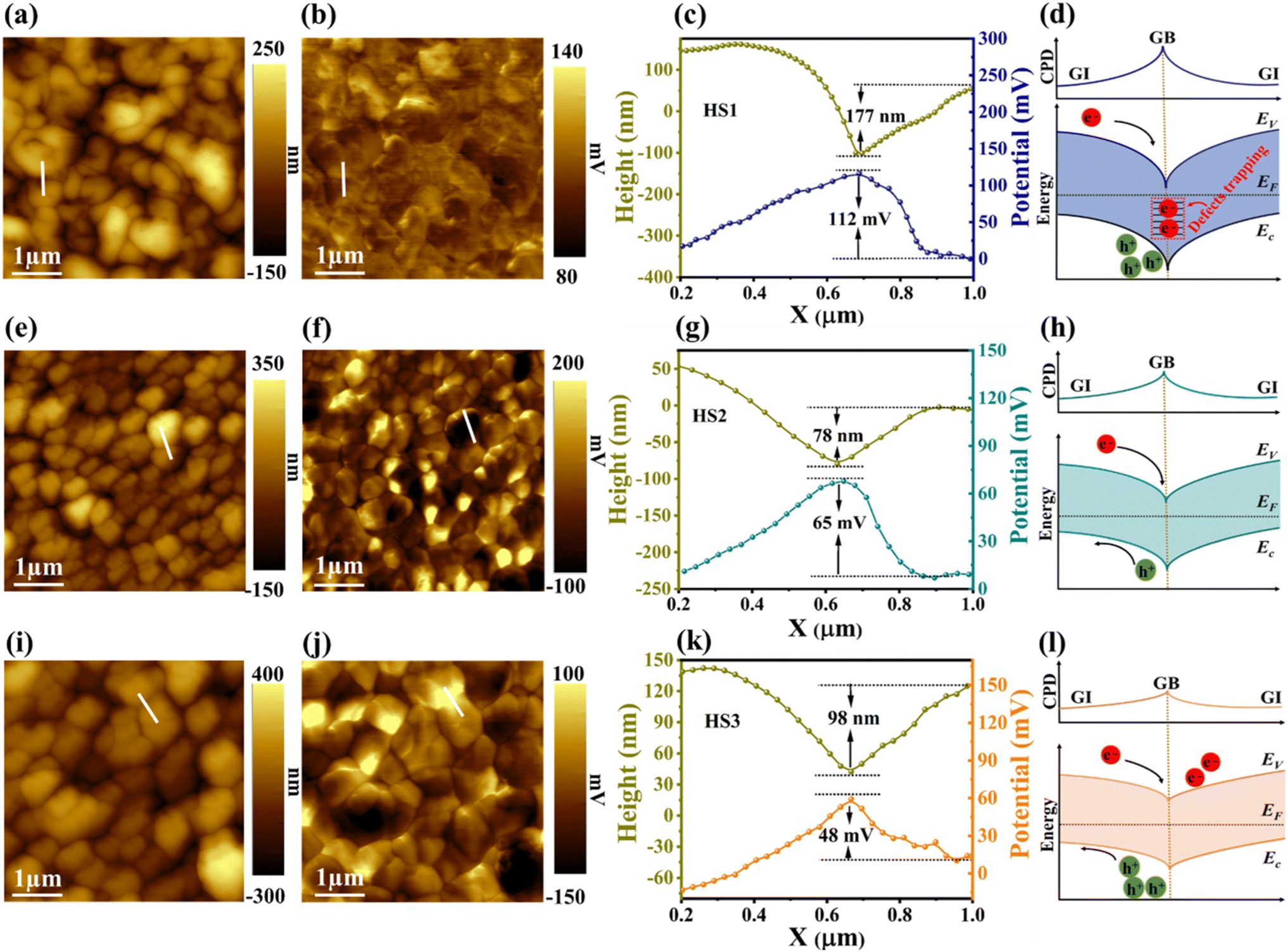 | ||
| Fig. 3 KPFM characterization of thin films from HS1 (a–d), HS2 (e–h), and HS3 (i–l) samples. (a) Topography, (b) surface potential, (c) topography and potential line profile scans and (d) a schematic band bending diagram, respectively. (e–h) and (i–l) The equivalent KPFM analysis of thin films from HS2 and HS3 samples. | ||
To further delve into the influence of dual back interface engineering, the reflection spectra of Sb2(S,Se)3 thin films were attained, employing a glass substrate and covering the 300–1500 nm wavelength range (Fig. S10a†). The spectrum clearly shows that the reflectance of the thin films from the HS2 and HS3 samples dropped gradually compared to those of HS1, especially in the shorter wavelength region. This can be associated with the evolution of surface compactness, crystallinity, and grain size, as validated by the SEM and XRD results.49 Additionally, there was a synchronized blue shift related to the absorption cut-off edge that inferred a modification in the band structure. Hence, the energy bandgap (Eg) was calculated according to Note S3,† and its values ranged from 1.226 to 1.231 eV (Fig. S10b†). This implies high composition-dependent adjustability and microstructure-dependent tolerance of band structures. Furthermore, the ideal low bandgap of Sb2(S,Se)3 enables efficient sunlight harvesting of a broad spectrum, marking it a desirable nominee for PEC photocathodes in solar hydrogen production. Alloying Sb2Se3 with Sb2S3 to form Sb2(S,Se)3 theoretically enables bandgap tuning between ∼1.1 eV (Sb2Se3) and ∼1.7 eV (Sb2S3) due to differences in electronegativity and atomic sizes. However, the limited bandgap change observed in this study with varying S/Se ratios is attributed to the non-linear bandgap behaviour of the alloy system, driven by complex atomic interactions. This non-linear bandgap shift, common in mixed chalcogenides, arises from factors like lattice strain and defect states, resulting in modest bandgap adjustments despite sulfur incorporation. Moreover, Mott–Schottky (M–S) characterization studies were performed to confirm the flat-band-potential (Efb) for Sb2(S,Se)3 thin films.47,50 The M–S characterization studies of thin films from HS1, HS2, and HS3 samples were also conducted (Fig. S11a–c†). This indicates that the 1/C2 declines with potential V. The obtained Efb values are approximately −0.074, 0.082, and 0.131 VNHE (for HS1, HS2, and HS3 films, respectively), showing that all three films are inherent p-type semiconductors.
3.2. PEC performance of Sb2(S,Se)3 photocathodes
The HS1, HS2, and HS3 films were used to fabricate the Mo/Sb2(S,Se)3/CdS/TiO2/Pt, Mo/MoO2/Sb2(S,Se)3/CdS/TiO2/Pt, and Mo/MoO2/Au/Sb2(S,Se)3/CdS/TiO2/Pt photocathode devices, respectively, and they were labelled as D-HS1, D-HS2, and D-HS3, respectively. Fig. 4a provides a schematic representation of the PEC measurement procedure. Under illumination, apparent hydrogen bubbles formed at the photocathode surface and moved towards the electrolyte (Fig. 4b1), implying a productive HER. With an area over 2 cm2 (Fig. 4b2), the as-prepared Sb2(S,Se)3 photocathode was quasi-homogeneous, indicating great potential in large-area application circumstances. As shown in Fig. 4b3, the champion device has an apparent layered structure of Mo/MoO2/Au/Sb2(S,Se)3/CdS/TiO2/Pt. The CdS buffer layer evenly covered the larger columnar and vertically grown grains in the Sb2(S,Se)3 layer. Between the interfaces of Mo/MoO2, MoO2/Au, Au/Sb2(S,Se)3, and Sb2(S,Se)3/CdS, a smooth and void-free contact is observed, which is advantageous for hindering any potential interfacial recombination loss. Using chopped light, the measured current density potential (J–V) curves of the D-HS1, D-HS2, and D-HS3 photocathodes are depicted in Fig. 4c, suggesting an increasing tendency in the current density. The photocathode HS1 based on pristine Mo lacked an appreciable PEC photo response with a very low cathodic Jph of ∼5.89 mA cm−2, as displayed in Fig. 4c. Chopped J–V curves of Mo(200 °C)/Sb2(S,Se)3/CdS/TiO2/Pt and Mo(300 °C)/Sb2(S,Se)3/CdS/TiO2/Pt photocathodes are also illustrated in Fig. 4d, showing a slight improvement in photocurrent density, corresponding to a Jph of ∼10.70 mA cm−2 and ∼13.50 mA cm−2, respectively. This indicates that the post-annealing process has increased the Mo substrates' wettability through a synchronous development in the MoO2 oxide layer, which changed the active sites, weakened the back contact barrier, and encouraged hole transportation on its surface. Remarkable improvement in Jph (∼18.80 mA cm−2) is noticeable upon further increasing the post-annealing temperature of the Mo substrate (400 °C/15 min), as observed in the D-HS2 photocathode (Fig. 4c). This infers that the photogenerated electron and hole pairs are effectively separated and transferred, consequently facilitating triggered electrochemical reactions at the interface between the electrode and electrolyte. Hence, the Mo substrates annealed at 200 °C and 300 °C were omitted from further analysis. The MoO2 oxide layer's functions include decreasing the back contact barrier, obtaining the preferable crystal orientation, encouraging grain growth, and lengthening the minority carrier diffusion length.35–37 Moreover, by introducing a thin underlayer of carrier transport channel Au on the post-annealed Mo substrate at 400 °C, the D-HS3 photocathode illustrated a dramatic increase in Jph (∼32.60 mA cm−2), as illustrated in Fig. 4c. As aforementioned, Au contributes to higher PEC performance by establishing different chemical bonds, recommending that the MoO2/Au/Sb2(S,Se)3 assemblage connected by Au–O and Au–S bonds can accomplish the synergy acceleration of surface active sites and carrier transport channels. Additionally, the dual back interface engineering through MoO2 and Au provides robust interfacial contact between Mo and Sb2(S,Se)3 thin films, leading to augmented carrier transport. As a result, it induces the suppression of interfacial charge recombination loss, improving charge transport and separation, and producing an exceptional improvement in the performance of the D-HS3 photocathode. This enhancement can also be associated with a superior absorber layer and crystal growth kinetics (i.e., the preferred (hkl) orientation) that prevent recombination loss and amplify carrier transport. | ||
| Fig. 4 (a) Schematic illustration of a PEC measurement using three electrodes. (b1) An image showing bubbles of hydrogen, (b2) a photograph of a representative 2 × 2 cm2 Sb2(S,Se)3-based photocathode, and (b3) the cross-sectional SEM photograph of the D-HS3 photocathode. (c) Chopped J–V curves of the D-HS1, D-HS2, and D-HS3 photocathodes. (d) Chopped J–V curves of the photocathodes based on a post-annealed (200 °C and 300 °C) Mo substrate in the dark and under chopped sunlight illumination. (e) J–V curves of the D-HS1, D-HS2, and D-HS3 photocathodes in the dark and under continuous sunlight illumination. (f) The measured HC-STH conversion efficiencies of the corresponding photocathodes and (g–i) the D-HS1, D-HS2, and D-HS3 photocathodes' statistical distribution and characterization of key performance. | ||
The linear swept current-density potential (J–V) of the D-HS1, D-HS2, and D-HS3 photocathodes under continuous and dark simulated sunlight illumination is displayed in Fig. 4e, depicting a similar variance upon the post-annealing of the Mo substrate at different temperatures and the integration of a thin carrier transport channel Au underlayer. The linear J–V and HC-STH conversion efficiencies for the excluded Mo substrate samples (200 °C and 300 °C) were also measured (Fig. S12a and b†). The corresponding HC-STH conversion efficiencies for D-HS1, D-HS2, and D-HS3 photocathodes were determined, as shown in Fig. 4f. The highest HC-STH values for the D-HS1, D-HS2, and D-HS3 devices are 0.30% at 0.159 VRHE, 2.04% at 0.199 VRHE, and 3.58% at 0.218 VRHE, respectively. Thus, Von was precisely measured by broadening the linearly swept J–V curves in the region where they are rapidly increasing. Consequently, the values of Von were positively shifted from 0.351 VRHE to 0.431 VRHE, which coordinated well with the fluctuations in Jph, implying a fully effective contribution to the HER. The samples containing a single back contact underlayer MoO2 (D-HS2) and dual back contact underlayers MoO2/Au (D-HS3) have a larger positive Von, which can be explained by the Sb2(S,Se)3 film's reduced defect density followed by the crystallographic orientation change, as confirmed by the XRD analysis (Fig. 2b).49 As shown in Fig. 3, for HS2 (D-HS2) and HS3 (D-HS3) thin films, the defect density was likewise decreased, because both samples exhibit a relatively equal dispersion of surface topography with high potential in comparison to HS1, indicating limited surface defects and fluctuating defect-induced potential, which is significantly beneficial for enhancing the PEC performance parameters such as Von and Jph. Moreover, the passivation of surface states is essential for improving charge separation and lowering recombination because they are known to function as trapping and recombination sites. Meanwhile, the bulk recombination centres formed by cation–anion defects are often suppressed by increasing the S content in materials like Sb2Se3 and Sb2(S,Se)3.6,51 The XPS (Fig. 2d–f; and Table S3†) and EDS studies show that the S concentration is slightly increased for both HS2 and HS3 samples, which encourages the suppression of bulk recombination centres even further to enhance Von. However, the limited improvement in the onset potential of Sb2(S,Se)3 compared to pristine Sb2Se3 is likely due to the complex defect chemistry in the mixed-anion system. Incorporating sulfur into Sb2Se3 can introduce shallow donor states, increasing recombination at grain boundaries and negatively affecting the onset potential. While sulfur incorporation might enhance charge carrier separation, it can also increase defect density or carrier recombination, leading to competing effects. The onset potential is influenced not only by the bandgap but also by surface states and recombination dynamics at the photocathode-electrolyte interface. Sulfur incorporation may alter the electronic structure or create additional recombination sites, offsetting potential gains in onset potential. It is noteworthy to mention that the finest values among the Sb2(S,Se)3 photocathodes are demonstrated in this work, with a maximum Jph (∼32.60 mA cm−2) and Von (∼0.431 VRHE). Fig. S13† shows the incident photon-to-current conversion efficiency (IPCE) spectra for Sb2(S,Se)3 photocathodes (D-HS1, D-HS2, and D-HS3), both with and without dual back-layer engineering, across 300–1000 nm. The D-HS3 device, which includes dual back underlayers (D-HS3), displays superior photon absorption and conversion, especially from 550 to 750 nm. Integrated photocurrents from the IPCE spectra are ∼5.10 mA cm−2 for D-HS1, ∼17 mA cm−2 for D-HS2, and ∼31.4 mA cm−2 for D-HS3, aligning well with Jph data from J–V measurements, though slightly lower due to the difference in conditions between chopped LSV and IPCE measurements such as calibration, wavelength of photons, size of the light source, etc. In parallel, the statistical distributions of the D-HS1, D-HS2, and D-HS3 photocathode performance parameters are shown in Fig. 4g–i. The dual back underlayers including MoO2 and carrier transport channel Au have a strong and credible positive impact on the performance of the D-HS3 photocathode. Table 1 compares key parameters of this study's champion Mo/MoO2/Au/Sb2(S,Se)3/CdS/TiO2/Pt photocathode to those of some of the best chalcogenide photocathodes that have been previously reported, including Sb2Se3, Sb2S3, and Sb2(S,Se)3.2,8,17,30,32,33,51,52 The comparison clearly shows that this device can achieve a comparable Von of ∼0.431 VRHE and ∼3.58% HC-STH efficiency, leading to a simultaneously superior Jph of 32.60 mA cm−2 amongst the Sb2(S,Se)3-based reported photocathodes so far. Moreover, the PEC performance of this device is analogous to that of other state-of-the-art chalcogenide-based (i.e., Sb2Se3) photocathodes presented at the top of the table.
| Photocathode | Electrolyte | J ph (mA cm−2 at 0 VRHE) | V on (VRHE) | HC-STH (%) | Ref. |
|---|---|---|---|---|---|
| FTO/Au/Sb2Se3/CdS/TiO2/SnO2 | 0.1 M H2SO4 | 29 | 0.50 | 3.8 | 33 |
| FTO/Au/Sb2Se3/PABA/TiO2/Pt | 0.1 M H2SO4 | 35 | 0.50 | 4.7 | 8 |
| Glass/Mo/Sb2Se3/CdS (In)/TiO2/Pt | 0.5 M H2SO4 | 35.7 | 0.54 | 5.6 | 2 |
| Mo/Sb2S3/CdS/TiO2/Pt | 0.5 M Na2SO4 | 6.0 | 0.50 | 0.64 | 32 |
| SLG/Mo/Ag:Sb2S3/CdS/Pt | 0.5 M Na2SO4 | 9.4 | 0.56 | 1.20 | 51 |
| SLG/Mo/Ag:Sb2S3/Al2O3/CdS/Pt | 0.5 M Na2SO4 | 13.0 | 0.68 | 2.78 | 52 |
| FTO/Au/Sb2S3/TiO2/Pt | 0.1 M H2SO4 | 22.5 | 0.52 | 0.69 | 17 |
| Mo/grad-S:Sb2Se3/TiO2/Pt | 1 M H2SO4 | 14.2 | 0.42 | 2 | 30 |
| FTO/Au/Sb2(S,Se)3/TiO2/Pt | 0.1 M H2SO4 | 16.5 | 0.44 | 1.1 | 17 |
| SLG/Mo/MoO2/Au/Sb2(S,Se)3/CdS/Pt | 0.5 M H2SO4 | 32.60 | 0.431 | 3.58 | This work |
Furthermore, efficient solar harvesting can also be stimulated by using such a perfect narrow bandgap. Therefore, the theoretical Jph of the Sb2(S,Se)3-based photocathodes was calculated using the absorbance (Fig. S14 and Note S4†), LHE (wavelength-dependent light harvesting efficiency) and AM 1.5G standard solar spectrum. Since the λe is ≈1070 nm, the Jph for D-HS3 is 40.80 mA cm−2 as portrayed in Fig. 5a, and 32.30 and 37.70 mA cm−2 for D-HS1 and D-HS2, respectively (Fig. S15a and b†). Moreover, the photocurrent transient method is a widely accepted approach for calculating charge transfer (ηtran) and charge separation (ηsep) efficiencies, particularly in photocathode systems. The following eqn (2) and (3), commonly used for this analysis, reliably reflect charge carrier dynamics when experimental parameters are well-controlled.2,47,52 This method provides valuable insights into interfacial processes without altering the experimental environment and offers a realistic assessment of charge separation and transfer under practical PEC water-splitting conditions, especially for Sb2(S,Se)3-based photocathodes. Fig. 5b displays the transient photocurrent attenuation spectra of the D-HS1, D-HS2, and D-HS3 photocathodes. The presence of the carrier recombination effect is evident in the D-HS1 photocathode, as it reveals an obvious “spike-like” transit under abrupt illumination. In contrast, the D-HS2 and D-HS3 photocathodes exhibit almost no “spike-like” transit, indicating boosted carrier transfer and attenuated charge recombination.7 The ηtran could be calculated using the determined photocurrents related to the “light off” and “light on” states due to the transient accumulation of charges at the electrode/electrolyte interface.53 In detail, the ηsep could be investigated as follows:47
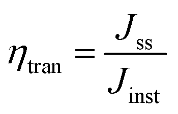 | (2) |
| Jph = Jabs × ηtran × ηsep | (3) |
 | ||
Fig. 5 (a) Energy density flux for the AM 1.5G standard solar spectrum and integrated photocurrent density of the HS3 sample. (b) Transient photocurrent response of D-HS1, D-HS2 and D-HS3 photocathodes. (c) Photocurrent stability test of the D-HS3 photocathodes (at 0 VRHE) for 3 h under illumination. (d) Nyquist and (e) Bode plots of the D-HS1, D-HS2 and D-HS3 photocathodes. (f) Schematic diagram along with the equivalent circuit system related to the charge carrier dynamics procedures. (g) Temperature-dependent Rs of the devices and the inset figure illustrates a circuit model. (h) Blocking contact barrier height determination of the PV-HS1, PV-HS2 and PV-HS3 photovoltaic devices using the temperature-dependent J–V measurement. (i) A![[thin space (1/6-em)]](https://www.rsc.org/images/entities/char_2009.gif) ln(J0) versus 1/kT plot of the corresponding photovoltaic devices. ln(J0) versus 1/kT plot of the corresponding photovoltaic devices. | ||
A similar Jph variation with Sb2(S,Se)3 film thickness is shown in the chopped J–T (photocurrent–density time) curves collected under AM 1.5G solar irradiation, indicating remarkable reversibility and stability (Fig. S16a–c†). Especially after operating for 3 h (Fig. 5c), the champion device D-HS3 retained around ∼94.7% of its Jph (∼30.9 mA cm−2), and even demonstrated the validity of hydrogen production after 6 h of operation (Movie S1, ESI†), indicating long-term stability. The literature suggests that partial photocorrosion of the CdS buffer layer occurs to some extent due to the assembly of injected charges, driven by thermodynamically favorable CdS redox transformations.54 The enhanced stability of the optimized D-HS3 device compared to D-HS1 and D-HS2 is primarily due to the synergistic effects of dual back interface engineering, which includes a MoO2 underlayer and a thin Au film. This design improves substrate wettability, enhances adhesion, and promotes a uniform, compact thin film, thereby reducing grain boundaries and defects that act as recombination centres. The MoO2 underlayer serves as a hole-blocking layer, minimizing charge carrier losses, while the Au underlayer provides an additional pathway for electron transport, further enhancing charge carrier separation and reducing recombination. In contrast, a clear decline in stability is evident for D-HS1 and D-HS2 photocathodes (Fig. S17a and b†). D-HS1 and D-HS2 show a rapid decrease in photocurrent density over time due to non-uniform thin films and poor back contact, which limits efficient charge carrier transport and increases recombination rates. Prolonged light exposure also contributes to photo-induced degradation in these samples, exacerbating performance loss (Movie S2†). Overall, the additional Mo/MoO2, MoO2/Au, and Au/Sb2(S,Se)3 junctions may have been advantageous since they enhanced the thin film's crystallinity, stability, and void-free interface, resulting in boosted carrier transportation, extraction, and collection efficiency. These optimizations are specifically accomplished through dual back interface engineering, which improves back contact modifications, promotes preferred Sb2(S,Se)3 crystal growth, and enhances the Sb2(S,Se)3/CdS heterojunction interface, ensuring the long-term stability of the D-HS3 photocathode.
The PEIS analysis of the Sb2(S,Se)3-based photocathodes was carried out to explore the specific charge carrier recombination and transfer features. Fig. 5d shows Nyquist plots with a single arc for D-HS1 and two arcs for the D-HS2 and D-HS3 photocathodes, illustrating consistency with the corresponding Bode diagrams (Fig. 5e), which include two regions with frequencies ranging from 10–100 kHz. In addition, Fig. 5f displays the schematic diagram and the analogous circuit system connected to the charge transfer procedure. Generally speaking, the bulk semiconductor capacitance (CHF) and the photoelectrode's internal charge transfer resistance (RHF) are affected by the PEIS-achieved high-frequency arc (≈103–105 Hz), the capacitance (CMF), and the charge capture resistance (RMF). Under the surface, trapping states in the bandgap are reflected by the middle-frequency arc (≈101–103 Hz), and the electrode and electrolyte interface's capacitance (CLF) and the resistance related to electro-chemical-charge-transfer reactions (RLF, e.g., HER) are indicated by the low-frequency arc (≈10−1–101 Hz).27 In this scenario, the low-frequency dependent resistor–capacitor (RLF–CLF) component cannot be clearly observed due to the high concentration of oxidizing species (H+) on the electrode surface and in the electrolyte. As a result, it is supposed that hydrogen would be generated by the transport of all photoelectrons towards the electrode or electrolyte and holes from the absorber at the substrate interface, demonstrating 100% Faraday efficiency. The PEIS data were fitted with an equivalent circuit design that consisted of two pairs of parallel resistor capacitors (R–C) and a series resistance (Rs). The Mo/Sb2(S,Se)3 back contact interface resistance is specifically responsible for the Rs; the space charge region's capacitance for the Sb2(S,Se)3/CdS heterojunction of these three devices is denoted by the RHF and CHF interfaces; and the associated charge transport resistance and the internal defect capacitance and resistance in Sb2(S,Se)3 films are represented by CMF and RMF, respectively. PEIS-fitted parameters for all three D-HS1, D-HS2, and D-HS3 photocathodes were determined (Table S4†), where the increased Rs values (∼3.2–3.8 Ω) specify a benign back contact interface, particularly by applying dual back interfacial layers of MoO2 and Au to enhance carrier transport and diminish recombination. The D-HS3 sample has an incredibly lower CHF value (∼1.18 × 10⁻⁶ F), implying that the charge accumulation occurs in a shorter time; the significantly lowered value of RHF (∼1.37 Ω) also recommends more efficient carrier separation and interface transportation. A remarkably lower RMF value of 5.04 Ω shows reduced bulk defects inside the D-HS3 absorber thin film due to an optimum connection between frequency and impedance at medium or low frequencies.
3.3. Analyzing the mechanisms of enhanced device performance
To gain a deeper understanding of these Mo/MoO2, MoO2/Sb2(S,Se)3, Au/Sb2(S,Se)3, and Sb2(S,Se)3/CdS heterojunction interfaces and their influence on the performance of photoelectric devices, the corresponding photovoltaic cells having identical device configurations (e.g., Mo/MoO2/Au/Sb2(S,Se)3/CdS/ITO/Ag) were prepared and denoted as PV-HS1, PV-HS2, and PV-HS3, respectively.Temperature-dependent measurements (J–V–T) were used in a dark environment in the temperature range of 200–300 K (Fig. S18a–c†) to further elucidate the sample's improved performance with the dual back interface modification. When the temperature decreased, the PV-HS1 device behaved like an open diode, but the devices (PV-HS2 and PV-HS3) that were treated with single or dual back interface layers continued to exhibit suppressed diode properties, indicating a decrease in the transfer barrier.55 To estimate temperature-dependent series-resistance (Rs), the specimen J–V–T curves are plotted in Fig. 5g. The Rs of the PV-HS1 sample grew drastically by about 11 times from 300–200 K, compared with the 5 and 3 times rise noted for the PV-HS2 and PV-HS3 samples, respectively. The deviation in Rs values with declining temperature implies that the background series resistance and the blocking barrier are responsible for the back contact barrier height, which confines charge transport.56 The inset photograph of Fig. 5g illustrates the device's back-contact junction model as a Schottky diode. Two diodes are included in the circuit model: the primary solar cell diode (DSC) and the back contact diode (DBC).37 The DBC is normally reverse biased when the DSC is forward biased; however, the reverse biased DBC is fairly detrimental to the production of photogenerated current. Consequently, the back contact barrier value is reduced by the dual back underlayers MoO2 and Au, greatly minimizing the detrimental effect of the reverse biased DBC on the photo-generated current output.
Furthermore, the back contact diode barrier height (ΦB) was determined by plotting ln(RsT) versus 1/T (Fig. 5h). The PV-HS2 sample's ΦB value was 107 meV, which was lower than the PV-HS1 device's (119 meV), implying that the PV-HS2 device has a lower barrier height. Moreover, the PV-HS3 dual back underlayer (MoO2 and Au) treatment produced a back contact barrier height of 80.1 meV, significantly improving charge transport and optimizing the device's performance. Generally, repressing the height of the back contact barrier is an important factor for augmenting carrier transport. J–V–T analysis can be used to ascertain the dominant recombination path present in devices by plotting Aln(J0) versus 1/kT, as shown in Fig. 5i. The activation energy (Ea) of interface recombination is normally approximated by using Aln(J0) vs. 1/kT, and its value can be attributed to as the predominance of both interface and bulk recombination.56 The PV-HS1 sample has an inferior Ea value of 1.08 eV compared with the bandgap, demonstrating the dominating interface recombination, while PV-HS2 and PV-HS3 devices have superior Ea values of 1.15 and 1.23 eV, respectively, which are in close proximity to the bandgap. As a result, interface recombination was greatly reduced by dual back interface layer modulation, improving junction quality and lowering the back contact barrier height.
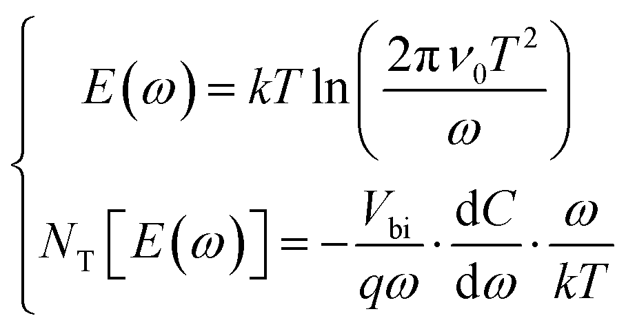
Admittance spectroscopy was performed to find out the influence of dual back interface engineering by incorporating an intermediate layer of MoO2 followed by carrier transport channel Au on the bulk defect properties. Fig. 6a, d and g show the C–f–T (temperature–dependent capacitance–frequency) of PV-HS1, PV-HS2, and PV-HS3 devices measured in varying temperature ranges of 340–110 K with 10 K increments and frequency ranges increasing from 102–106 Hz. Only one defect level can be identified against frequency, indicating that only one type of defect can be found. The inflection frequencies (ω0 = 2πf0) were obtained through the angular frequency point ω at the maximum value of the plot of ωdC/dω. The slopes of a linear fit of the Arrhenius plots were used to determine the defect activation energies based on the following equation:48
 | (4) |
 | (5) |
 | ||
| Fig. 6 Characterization of temperature-dependent admittance spectroscopy for Sb2(S,Se)3 photovoltaic devices. (a, d and g) Variation of capacitance at different frequencies and temperatures. (b, e and h) Using the Arrhenius plots of the characteristic frequencies to acquire the defect activation energy. (c, f and i) Defect distributions of PV-HS1, PV-HS2 and PV-HS3 devices. | ||
To determine the influence of interfacial recombination, deep-level capacitance profiling (DLCP) and capacitance–voltage (C–V) profiling measurements were performed, and the results are displayed in Fig. 7a and b. Bulk defects, interfacial defects, and free carriers are all included in the doping density NC–V determined by the C–V profiling, whereas only free carriers and bulk defects are included in the doping density NDLCP determined by DLCP. The following formulae can be used to get the NC–V and NDLCP plots versus the profiling width x:36
 | (6) |
 | (7) |
 | (8) |
 | ||
| Fig. 7 (a) C–V and DLCP profiles. (b) 1/C2–V graphs of the PV-HS1, PV-HS2, and PV-HS3 photovoltaic devices. Electrical behaviours of the corresponding three devices: (c) dark J–V curves, (d) characterization of the shunt conductance G, (e) the series resistance R, the ideality factor A, and (f) the current density Jsc for reverse saturation. The band diagrams of D-HS1 (g), D-HS2 (h), and D-HS3 (i) devices. | ||
The dJ/dV against V plot is depicted in Fig. 7d. The obtained G values of PV-HS1, PV-HS2, and PV-HS3 devices were 4.10, 2.24, and 0.51 mS cm−2, respectively. The devices' two parameters, A and R, were determined by comparing dV/dJ to (J + JSC)−1, as shown in Fig. 7e. For the PV-HS1, PV-HS2, and PV-HS3 devices, the observed values of R were 10.0, 6.11, and 3.66 Ω cm2, respectively. The obtained R value for the PV-HS3 device was lower than that of PV-HS2, while the R value of PV-HS2 was lower than that of PV-HS1. Furthermore, the resulting A values for PV-HS1, PV-HS2 and PV-HS3 devices were 1.79, 1.55 and 1.14, respectively, inferring that the PV-HS3 device had less interface recombination. Plotting the ln(J + JSC − GV) vs. V–RJ yielded the J0 values of 3.39 × 10⁻³, 2.36 × 10⁻⁴ and 1.42 × 10⁻⁴ mA cm−2 for the PV-HS1, PV-HS2, and PV-HS3 samples, respectively (Fig. 7f). The R and A values among the PV-HS1 device and dual back interface engineering treated devices, including PV-HS2 and PV-HS3 devices, suggested a drop in defect recombination at the interfaces and in bulk areas. Moreover, a reduced value of J0 was noted in the PV-HS3 device, demonstrating a decline in deep-level defect concentration and corresponding mitigation in nonradiative recombination loss.37
The D-HS1 device's Mo/Sb2(S,Se)3 interface barrier was further examined because the higher back contact barriers may have contributed to its inferior performance. The schematic band diagrams of D-HS1, D-HS2 and D-HS3 photocathodes are displayed in Fig. 7g–i. The UPS spectra of Mo, MoO2, Au and Sb2(S,Se)3 thin films are displayed in Fig. S19a–d†. The magnified binding energy in the 7.4–6.8 eV region is shown as the inset figures in each graph (Fig. S19†). The barrier heights of Mo/Sb2(S,Se)3, Mo/MoO2, MoO2/Au and Au/Sb2(S,Se)3 were 0.39, 0.21, 0.18 and 0.07 eV, respectively (Fig. 7g–i). The UPS analysis proves that, of the three devices, D-HS3 has the best performance and superior carrier collection efficiency since it has a lower barrier height compared to D-HS2 and D-HS1. Improved crystalline quality, crystal orientation, and the lowered barrier height all assisted in the boosted Jph and higher HC-STH efficiency. The Sb2(S,Se)3 band gaps in D-HS1, D-HS2, and D-HS3 devices were 1.226, 1.227, and 1.231 eV, respectively (Fig. S10b†). The band gap of the Sb2(S,Se)3 absorber can possibly be altered by both MoO2 and Au underlayers. Overall, incorporating both the intermediate layer of MoO2 and carrier transport channel Au interface layers plays several functions, such as facilitating grain growth, achieving the preferred (hkl) orientation of Sb2(S,Se)3, increasing the minority carrier diffusion length, superior carrier collection and separation efficiency and decreasing the back contact barrier. These optimized parameters are certainly the primary factors contributing to the photocathode's elevated performance.
4. Conclusion
In summary, this work employed a dual back interface engineering approach by incorporating an intermediate layer of MoO2 and a secondary carrier transport channel of Au to strengthen the charge carrier dynamics in Sb2(S,Se)3 photocathodes. The synergistic assembly of dual back underlayers efficiently improved the crystal growth and the preferential orientation in the Sb2(S,Se)3 absorber layer by improving the Mo substrate's wettability. Additionally, back contact barrier height, and bulk and interface defects were significantly suppressed, leading to inhibited charge carrier recombination loss. As a result, the synergy of MoO2 and Au dual back interface layers produced a remarkable improvement in charge separation and transport efficiency, as well as lengthened minority carrier diffusion length and depletion width in Sb2(S,Se)3 photocathodes. Therefore, comparing the untreated D-HS1 device and the D-HS3 photocathode with dual back interface engineering modification, the Jph was enhanced from ∼5.89 mA cm−2 to ∼32.60 mA cm−2, Von improved from ∼0.351 VRHE to ∼0.431 VRHE, and HC-STH conversion efficiency significantly increased from ∼0.30% to ∼3.58%. This work offers great potential of interface engineering for the fabrication of highly efficient chalcogenide thin-film photocathodes.Data availability
The data supporting this article have been included as part of the ESI.†Author contributions
Hafiz Sartaj Aziz: data curation, investigation, methodology, conceptualization, writing – original draft. Tahir Imran: methodology, writing – original draft, investigation. Munir Ahmad: investigation, writing – original draft. Guo-Jie Chen: data curation, formal analysis. Ping Luo: data curation, investigation. Dong-Lou Ren: data curation, investigation. Bing-Suo Zou: data curation, investigation. Ju-Guang Hu: investigation, methodology. Zheng-Hua Su: visualization, validation. Pei-Guang Yan: supervision, visualization, validation. Guang-Xing Liang: conceptualization, supervision, visualization, validation writing – review & editing. Shuo Chen: conceptualization, formal analysis, writing – review & editing, supervision, funding acquisition.Conflicts of interest
There are no conflicts to declare.Acknowledgements
This work was supported by the National Natural Science Foundation of China (No. 62474114 and 62104156), Guangdong Basic and Applied Basic Research Foundation (2023A1515011256) China, and Shenzhen Science and Technology Program (GJHZ20240218113809019 and 20231122102326002) China. This project was also supported by an open foundation of Guangxi Key Laboratory of Processing for Non-ferrous Metals and Featured Materials, Guangxi University (Grant No. 2022GXYSOF13). The authors are grateful for Prof. Yu-Jia Zeng's assistance with KPFM characterization, at Shenzhen University.References
- G. Xiao, X. Ren, Y. Hu, Y. Cao, Z. Li, Z. Shi and F. Jiang, ACS Energy Lett., 2024, 9, 715–726 CrossRef CAS.
- S. Chen, T. Liu, M. Chen, M. Ishaq, R. Tang, Z. Zheng, Z. Su, X. Li, X. Qiao and P. Fan, Nano Energy, 2022, 99, 107417 CrossRef CAS.
- S. Wang, S. Feng, B. Liu, Z. Gong, T. Wang and J. Gong, Chem. Sci., 2023, 14, 2192–2199 RSC.
- Y. Xia, M. Zhu, L. Qin, C. Zhao, D. Hong, Y. Tian, W. Yan and Z. Jin, Energy Mater., 2023, 3, 300004 CrossRef CAS.
- F. Amano and K. Tsushiro, Energy Mater., 2024, 4, 400006 CAS.
- Y. Li, K. Wang, D. Huang, L. Li, J. Tao, N. A. A. Ghany and F. Jiang, Appl. Catal., B, 2021, 286, 119872 CrossRef CAS.
- G. Liang, T. Liu, M. Ishaq, Z. Chen, R. Tang, Z. Zheng, Z. Su, P. Fan, X. Zhang and S. Chen, Chem. Eng. J., 2022, 431, 133359 CrossRef CAS.
- J. Tan, W. Yang, H. Lee, J. Park, K. Kim, O. S. Hutter, L. J. Phillips, S. Shim, J. Yun, Y. Park, J. Lee, J. D. Major and J. Moon, Appl. Catal., B, 2021, 286, 119890 CrossRef CAS.
- R. Zhou, X. Li, L. Wan, H. Niu, H. Wang, X. Yang, X. Wang, J. Hou, J. Xu and B. Xu, Adv. Funct. Mater., 2024, 34, 2308021 CrossRef CAS.
- K. Li, Z. Cai, J. Yang, H. Wang, L. Zhang, R. Tang, C. Zhu and T. Chen, Adv. Funct. Mater., 2023, 33, 2304141 CrossRef CAS.
- X. Chen, B. Che, Y. Zhao, S. Wang, H. Li, J. Gong, G. Chen, T. Chen, X. Xiao and J. Li, Adv. Energy Mater., 2023, 13, 2300391 CrossRef CAS.
- J. Dong, H. Liu, L. Ding, B. Che, P. Xiao, Z. Cao, Y. Liu, L. Lou, R. Tang and J. Luo, Adv. Funct. Mater., 2023, 34, 2309764 CrossRef.
- M. Xiao, Z. Wang, K. Maeda, G. Liu and L. Wang, Chem. Sci., 2023, 14, 3415–3427 RSC.
- M. A. Steiner, R. M. France, J. Buencuerpo, J. F. Geisz, M. P. Nielsen, A. Pusch, W. J. Olavarria, M. Young and N. J. E. Daukes, Adv. Energy Mater., 2021, 11, 2002874 CrossRef CAS.
- C. Chen and J. Tang, ACS Energy Lett., 2020, 5, 2294–2304 CrossRef CAS.
- Z. Duan, X. Liang, Y. Feng, H. Ma, B. Liang, Y. Wang, S. Luo, S. Wang, R. E. Schropp and Y. Mai, Adv. Mater., 2022, 34, 2202969 CrossRef CAS.
- W. Qiu, R. Lei, X. Tang, Y. Tang, X. Huang, K. Zhang, Z. Lin, S. Xiao, X. Wang and S. Yang, Sol. RRL, 2024, 8, 2300876 CrossRef CAS.
- X. Hu, J. Tao, R. Wang, Y. Wang, Y. Pan, G. Weng, X. Luo, S. Chen, Z. Zhu and J. Chu, J. Power Sources, 2021, 493, 229737 CrossRef CAS.
- Y. Zhao, S. Wang, C. Li, B. Che, X. Chen, H. Chen, R. Tang, X. Wang, G. Chen and T. Wang, Energy Environ. Sci., 2022, 15, 5118–5128 RSC.
- R. Tang, X. Wang, W. Lian, J. Huang, Q. Wei, M. Huang, Y. Yin, C. Jiang, S. Yang and G. Xing, Nat. Energy, 2020, 5, 587–595 CrossRef CAS.
- J. Tan, X. Zhang, J. Suh, N. Ha, J. Lee, S. D. Tilley and W. Yang, Mater. Today Energy, 2023, 34, 101288 CrossRef CAS.
- X. Wang, R. Tang, C. Jiang, W. Lian, H. Ju, G. Jiang, Z. Li, C. Zhu and T. Chen, Adv. Energy Mater., 2020, 10, 2002341 CrossRef CAS.
- J. Kim, W. Yang, Y. Oh, H. Lee, S. Lee, H. Shin, J. Kim and J. Moon, J. Mater. Chem. A, 2017, 5, 2180–2187 RSC.
- W. Yang, J. H. Kim, O. S. Hutter, L. J. Phillips, J. Tan, J. Park, H. Lee, J. D. Major, J. S. Lee and J. Moon, Nat. Commun., 2020, 11, 861 CrossRef CAS.
- H. Lee, W. Yang, J. Tan, Y. Oh, J. Park and J. Moon, ACS Energy Lett., 2019, 4, 995–1003 CrossRef CAS.
- J. Tan, W. Yang, Y. Oh, H. Lee, J. Park and J. Moon, ACS Appl. Mater. Interfaces, 2018, 10, 10898–10908 CrossRef CAS.
- J. Tan, W. Yang, Y. Oh, H. Lee, J. Park, R. Boppella, J. Kim and J. Moon, Adv. Energy Mater., 2019, 9, 1900179 CrossRef.
- Y. Cheng, C. Xin, J. Zhao, J. Wang, M. Gong, H. Miao and X. Hu, Electrochim. Acta, 2022, 403, 139610 CrossRef CAS.
- X. Liu, L. Zhang, W. Jin, Q. Li, Q. Sun, Y. Wang, E. Liu, X. Hu and H. Miao, Chem. Eng. J., 2023, 475, 146315 CrossRef CAS.
- H. Zhou, M. Feng, M. Feng, X. Gong, D. Zhang, Y. Zhou and S. Chen, Appl. Phys. Lett., 2020, 116, 113902 CrossRef.
- Y. Wang, R. Liang, C. Qin, L. Ren, Z. Ye and L. Zhu, Sustainable Energy Fuels, 2021, 5, 855–861 RSC.
- Y. C. Wang, Y. Y. Zeng, L. H. Li, C. Qin, Y. W. Wang, Z. R. Lou, F. Y. Liu, Z. Z. Ye and L. P. Zhu, ACS Appl. Energy Mater., 2020, 3, 6188–6194 CrossRef CAS.
- W. Yang, J. Park, H. C. Kwon, O. S. Hutter, L. J. Phillips, J. Tan, H. Lee, J. Lee, S. D. Tilley, J. D. Major and J. Moon, Energy Environ. Sci., 2020, 13, 4362–4370 RSC.
- G. J. Chen, R. Tang, S. Chen, Z. H. Zheng, Z. H. Su, H. L. Ma, X. H. Zhang, P. Fan and G. X. Liang, ACS Appl. Mater. Interfaces, 2022, 14, 31986–31997 CrossRef CAS.
- T. J. Huang, X. Yin, G. Qi and H. Gong, Phys. Status Solidi RRL, 2014, 8, 735–762 CrossRef CAS.
- R. Tang, S. Chen, Z. H. Zheng, Z. H. Su, J. T. Luo, P. Fan, X. H. Zhang, J. Tang and G. X. Liang, Adv. Mater., 2022, 34, 2109078 CrossRef CAS.
- J. Lin, G. Chen, N. Ahmad, M. Ishaq, S. Chen, Z. Su, P. Fan, X. Zhang, Y. Zhang and G. Liang, J. Energy Chem., 2023, 80, 256–264 CrossRef CAS.
- Y. Feng, J. Liu, H. Li, J. Deng and Y. Liu, Ultrason. Sonochem., 2023, 97, 106469 CrossRef CAS.
- F. Foadi, G. H. ten Brink, M. R. Mohammadizadeh and G. Palasantzas, J. Appl. Phys., 2019, 125, 244307 CrossRef.
- W. J. Liu, Y. H. Chang, C. L. Fern, Y. T. Chen, T. Y. Jhou, P. C. Chiu, S. H. Lin, K. W. Lin and T. H. Wu, Coatings, 2021, 11, 1268 CrossRef CAS.
- Z. Liu, D. Jiang, L. Yang, J. Yu, X. Li, X. Liu, L. Zhao, X. L. Zhang, F. Han, W. Zhou and L. Hong, Nano Energy, 2021, 88, 106302 CrossRef CAS.
- S. Wang, P. Liu, C. Meng, Y. Wang, L. Zhang, L. Pan, Z. Yin, N. Tang and J. J. Zou, J. Catal., 2022, 408, 196–205 CrossRef CAS.
- S. Y. Kim, S. H. Kim, S. Hong, D. H. Son, Y. I. Kim, S. Kim, K. Ahn, K. J. Yang, D. H. Kim and J. K. Kang, ACS Appl. Mater. Interfaces, 2019, 11, 23160–23167 CrossRef CAS.
- M. Ishaq, H. Deng, U. Farooq, H. Zhang, X. Yang, U. A. Shah and H. Song, Sol. RRL, 2019, 3, 1900305 CrossRef CAS.
- Y. Zhou, L. Wang, S. Chen, S. Qin, X. Liu, J. Chen, D. J. Xue, M. Luo, Y. Cao and Y. Cheng, Nat. Photonics, 2015, 9, 409–415 CrossRef CAS.
- Y. Xiang, H. Guo, Z. Cai, C. Jiang, C. Zhu, Y. Wu, W. H. Zhu and T. Chen, Chem. Commun., 2022, 58, 4787–4790 RSC.
- G. Liang, Z. Li, M. Ishaq, Z. Zheng, Z. Su, H. Ma, X. Zhang, P. Fan and S. Chen, Adv. Energy Mater., 2023, 13, 2300215 CrossRef CAS.
- P. Luo, T. Imran, D. L. Ren, J. Zhao, K. W. Wu, Y. J. Zeng, Z. H. Su, P. Fan, X. H. Zhang and G. X. Liang, Small, 2024, 20, 2306516 CrossRef CAS PubMed.
- G. Liang, M. Chen, M. Ishaq, X. Li, R. Tang, Z. Zheng, Z. Su, P. Fan, X. Zhang and S. Chen, Adv. Sci., 2022, 9, 2105142 CrossRef CAS.
- H. Dotan, K. Sivula, M. Grätzel, A. Rothschild and S. C. Warren, Probing the photoelectrochemical properties of hematite (α-Fe2O3) electrodes using hydrogen peroxide as a hole scavenger, Energy Environ. Sci., 2011, 4, 958–964 RSC.
- M. Yang, Z. Fan, J. Du, R. Li, D. Liu, B. Zhang, K. Feng, C. Feng and Y. Li, ACS Catal., 2022, 12, 8175–8184 CrossRef CAS.
- M. Yang, Z. Fan, J. Du, C. Feng, R. Li, B. Zhang, N. Pastukhova, M. Valant, M. Finšgar, A. Mavrič and Y. Li, Small, 2024, 20, 2311644 CrossRef CAS PubMed.
- D. Klotz, D. A. Grave and A. Rothschild, Phys. Chem. Chem. Phys., 2017, 19, 20383–20392 RSC.
- B. Weng, M. Y. Qi, C. Han, Z. R. Tang and Y. J. Xu, ACS Catal., 2019, 9, 4642–4687 CrossRef CAS.
- G. Chen, Y. Luo, M. Abbas, M. Ishaq, Z. Zheng, S. Chen, Z. Su, X. Zhang, P. Fan and G. Liang, Adv. Mater., 2024, 36, 2308522 CrossRef CAS.
- Y. Zhao, Z. Yu, J. Hu, Z. Zheng, H. Ma, K. Sun, X. Hao, G. Liang, P. Fan and X. Zhang, J. Energy Chem., 2022, 75, 321–329 CrossRef CAS.
- C. Liu, S. Wu, Y. Gao, Y. Feng, X. Wang, Y. Xie, J. Zheng, H. Zhu, Z. Li and R. E. Schropp, Adv. Funct. Mater., 2022, 32, 2209601 CrossRef CAS.
Footnote |
| † Electronic supplementary information (ESI) available. See DOI: https://doi.org/10.1039/d4sc05893c |
| This journal is © The Royal Society of Chemistry 2025 |