
 Open Access Article
 This Open Access Article is licensed under a Creative Commons Attribution-Non Commercial 3.0 Unported Licence
Enhanced sodium-ion intercalation and migration in boron/carbon-doped WS2/graphene bilayers: insights from electronic structure calculations†
Thi Nhan Tran *a,
Nguyen Hoang Sonbc,
Nguyen Minh Hieuc,
Thuy Trang Nguyenbd,
Yoshiyuki Kawazoeefg,
Luong Huu Duch,
Minh Triet Dangi,
Phi Long Nguyena and
Viet Bac Phung Thi*c
*a,
Nguyen Hoang Sonbc,
Nguyen Minh Hieuc,
Thuy Trang Nguyenbd,
Yoshiyuki Kawazoeefg,
Luong Huu Duch,
Minh Triet Dangi,
Phi Long Nguyena and
Viet Bac Phung Thi*c
aHanoi University of Industry, 298 Cau Dien Street, Bac Tu Liem, Hanoi 100000, Vietnam. E-mail: tran.nhan@haui.edu.vn
bFaculty of Physics, University of Science, Vietnam National University – Hanoi, Hanoi, Vietnam
cCenter for Environmental Intelligence and College of Engineering & Computer Science, VinUniversity, Hanoi 100000, Vietnam
dKey Laboratory for Multiscale Simulation of Complex Systems, University of Science, Vietnam National University – Hanoi, Hanoi, Vietnam
eNew Industry Creation Hatchery Center, Tohoku University, Sendai, 980-8579, Japan
fDepartment of Physics and Nanotechnology, SRM Institute of Science and Technology, Kattankulathur 603203, Tamil Nadu, India
gSchool of Physics, Institute of Science, Suranaree University of Technology, 111 University Avenue, Nakhon Ratchasima 30000, Thailand
hLaboratory for Chemistry and Life Science (CLS), Institute of Integrated Research (IIR), Institute of Science Tokyo (Science Tokyo), R1-25, 4259 Nagatsuta-cho, Midori-ku, Yokohama, 226-8501, Japan
iSchool of Education, Can Tho University, Can Tho City 900000, Vietnam
First published on 14th July 2025
Abstract
Heterostructures composed of graphene (G) and WS2 have recently been proposed as a promising new two-dimensional carbon allotrope for an anode material in sodium-ion batteries. Actively controlling material defects by substituting sulfur (S) atoms on the surface of WS2 with alternative dopants is anticipated to be a potential strategy for enhancing the electrochemical performance of WS2/G heterostructures. Here, we employ first-principles density functional theory (DFT) calculations to systematically investigate the impact of boron (B) and carbon (C) doping on the sodium intercalation and diffusion mechanisms within the heterostructures. The results reveal that doped WS2/G heterostructures show electronic characteristics of metallic materials, which are beneficial for their application as high-performance anode materials. The introduction of B/C dopants significantly enhance the binding affinity for sodium intercalation at active sites, both on the surface and at interfacial region, with binding energies reaching up to −1.702 eV, which can mitigate sodium dendrite formation during electrochemical cycling. Notably, the presence of B/C dopants can create energetically favorable diffusion pathway both on the surface and in the interfacial region of the WS2/G bilayers for sodium ions with energy barriers ranging from 0.091 to 0.494 eV, underscoring their potential to support high-rate charge/discharge processes. Additionally, B/C-doped WS2/G heterostructures exhibit inconsiderably structural deformation during sodium intercalation, making them suitable candidates as anode materials in batteries with high cycling stability. Our findings provide valuable insights into the effect of the dopants within the sodium intercalation mechanisms of WS2/G heterostructures, paving the way for the rational design of next-generation anode materials for high-performance sodium-ion batteries.
Introduction
Lithium-ion rechargeable batteries are experiencing massive growth due to the enormous demand for portable mobile devices and electric vehicles.1 However, the rapid increase in lithium battery manufacturing is placing heavy pressure on lithium stocks, potentially leading to a lithium shortage and cost increases in the foreseeable future.2 Several recent reports have highlighted progress in developing alternative electrochemical batteries.3–5 Sodium-ion batteries (SIBs) have emerged as a promising alternative generation that can replace lithium-ion batteries because of sodium's natural abundance, low cost, and environmental benignity.4 However, the larger ionic radius of sodium ions compared to lithium ions cause several drawbacks for SIBs, such as slow diffusion, the limitation of energy storage density, and large internal stress of the electrode materials. To address this challenge, finding anode materials that possess adequate electrochemical capacity and cyclic stability for a sodium ion insertion reaction and implementing strategies to enhance Na-ion diffusion while mitigating structural degradation during the Na-ion insertion process is necessary.5Developing and optimizing advanced anode materials for SIBs has been an area of growing interest. Previous research indicates that WS2 monolayer (ML) possesses several attractive properties for SIBs, including high stability, reversibility, and a suitable adsorption environment for sodium-ions, thanks to the tuneable dimensions of interfacial spacing and the precise nanostructure.6 Despite these advantages for SIBs, WS2 ML exhibits low-rate capability, low electronic conductivity, slow diffusion of Na ions, and considerable volume expansion during sodiation/desodiation processes, leading to quick capacity fading.7
Vertically stacking on graphene to form heterostructures has been proposed as a promising strategy to enhance the performance of transition metal dichalcogenide (TMD) ML as anode materials in SIBs.7,8 This approach enhances electrical conductivity without requiring a metallic substrate, conducting additives, or polymeric binders of heterostructures.8–18 Moreover, the graphene matrix of the heterostructures can effectively buffer the volume change during the Na insertion/extraction process and increase the anode's overall electrochemical function.10,12 In recent studies, WS2/G heterostructures have been successfully synthesized through ultrasonication, chemical vapor deposition, and hydrothermal techniques, achieving uniform growth of WS2 nanocrystals on graphene nanosheets.8,12,14 It was used as an anode material for both lithium-ion batteries and SIBs due to its high surface area and good in-plane conductivity, which facilitates fast electron transfer during electrochemical reactions of the material.12,13,16–18 As electrodes in SIBs, the WS2/G exhibits a good reversible sodium storage capacity of about 590 mA h g−1.12 It also shows excellent high-rate performance and cyclability.
With the aim of developing and optimizing advanced anode materials based on WS2/G composites for SIBs, several rational strategies have been proposed from both experimental and theoretical perspectives. One effective approach involves rolling graphene into hollow nanotubes to encapsulate WS2 nanostructures, thereby constructing a highly conductive and electrolyte-accessible framework. This architecture not only facilitates electron and ion transport but also effectively mitigates volume changes during cycling.19 Another promising design introduces a three-layer shell structure composed of a stable porous carbon shell, WS2 nanosheets, and nitrogen-doped graphene, which significantly enhances lithium and sodium storage performance. This configuration delivers a high discharge capacity of 205 mA h g−1 after 900 cycles at 0.5 A g−1 for SIBs.20 It was reported that co-doping with nitrogen and oxygen modifies the electronic structure of WS2, reducing its bandgap from 1.6 eV to 0 eV and increasing the interlayer spacing in WS2/G composites. These modifications significantly improve electron and ion transport, resulting in exceptional electrochemical performance with an ultrafast Na+ storage capability and remarkable cycling stability over 3000 cycles.21 Additionally, substituting the sulfur atoms in WS2 or MoS2 ML, another two-dimensional material in the TMD family, with boron/carbon (B/C) has been proposed as an effective pathway to increase electronic conductivity, enhance sodium intercalation strength, and accelerate diffusion of electrons and ions.22–25 Similarly, dopants on the sulfur layer of the WS2/G heterostructure are expected to modify the surface properties by creating additional active sites for sodium intercalation, thereby improving the storage capacity of SIBs.
A good understanding of the dopant effect on the sodium intercalation mechanism and sodium migration within WS2/G heterostructures is critical to boost their application as new nanoscale anodes for high-performance SIBs. Hence, we perform a systematic first-principles study to explore the impact of boron (B) and carbon (C) doping on Na intercalation mechanism and diffusion in WS2/G heterostructures for potential use as anode materials in SIBs. We focus on analysing the effect of B/C dopants on sodium intercalation ability, electronic conductivity, structural stability, and Na-ionic migration characteristics of the WS2/G heterostructures. Our findings provide a meaningful and promising strategy for designing advanced SIB anodes.
Computational details
We performed density functional theory (DFT) calculations with the projector-augmented wave and plane-wave basis set as implemented in the Vienna Ab initio Simulation Package (VASP).26,27 The generalized gradient approximation of the Perdew–Burke–Ernzerhof functional method28 was used to treat the exchange correlation energy between Na and the doped WS2/G bilayers. To describe the interlayer interactions between graphene and doped WS2 monolayer, the van der Waals correction implemented in the functional optB88-vdW29 is introduced in the calculations.To achieve a heterostructure with a minor lattice mismatch, we constructed a bilayer based on a 4 × 4 × 1 supercell of WS2 monolayer stacked above a 5 × 5 × 1 supercell of graphene, to investigate the Na intercalation mechanism of the C/B-doped WS2/G heterostructures. A Monkhorst–Pack scheme30 with 6 × 6 × 1 and 9 × 9 × 1 k-mesh is required to converge the plane-wave basis set for the optimization and electronic calculations of the doped WS2/G heterostructures, respectively. A convergence energy of 540 eV was applied to all investigated samples. The change in the total energy between the two consecutive steps is set to be 10−5 eV. Atomic positions are relaxed until the maximum residual force acting on each atom is smaller than 0.01 eV Å−1. A vacuum of 25 Å thickness was introduced between two neighbouring heterostructures to eliminate the atomic interactions between the imaged periodic systems. We utilized the VASPKIT package31 to post-process the electronic properties.
We computed the Na binding energy (Eads) for each explored configuration using the following relation:
| Ebind = Ecomplex − Edop − ENa, | (1) |
| Δρ = ρcomplex − ρdop − ρNa, | (2) |
Results and discussions
Geometric structure
Fig. S1† presents the optimized structure of the 4![[thin space (1/6-em)]](https://www.rsc.org/images/entities/char_2009.gif) :5 pristine WS2/G heterostructures and Table 1 summarizes the structural parameters and interlayer binding energy of the isolated WS2 and graphene layers and the pristine WS2/G heterostructures, which agree well with previous experimental and theoretical works.35–38 It can be found that the lattice mismatch between the WS2 and graphene layers is 2.6%, comparable to the other heterostructures, such as graphene/hexagonal boron nitride.39 In the heterostructure, the C–C bond length is elongated by 0.6%, while the W–S bond length undergoes a compression of 0.4%. The strains sustained by the component materials upon the formation of the heterostructure are calculated using the following equation:
:5 pristine WS2/G heterostructures and Table 1 summarizes the structural parameters and interlayer binding energy of the isolated WS2 and graphene layers and the pristine WS2/G heterostructures, which agree well with previous experimental and theoretical works.35–38 It can be found that the lattice mismatch between the WS2 and graphene layers is 2.6%, comparable to the other heterostructures, such as graphene/hexagonal boron nitride.39 In the heterostructure, the C–C bond length is elongated by 0.6%, while the W–S bond length undergoes a compression of 0.4%. The strains sustained by the component materials upon the formation of the heterostructure are calculated using the following equation:
 | (3) |
| Isolated WS2 | Isolated graphene | Pristine heterostructure | B-doped heterostructure | C-doped heterostructure | |
|---|---|---|---|---|---|
| Lateral lattice constant | a = b = 12.66 Å | a = b = 12.34 Å | a = b = 12.46 Å | a = b = 12.46 Å | a = b = 12.46 Å |
| W–S bond length (Å) | 2.42 | — | 2.41 | 2.41 | 2.41 |
| C–W bond length (Å) | — | — | — | — | 2.02 |
| B–W bond length (Å) | — | — | — | 2.12 | — |
| C–C bond length (Å) | — | 1.43 | 1.44 | 1.44 | 1.44 |
| Strain sustained by WS2 layer (%) | — | — | 1.57 | 1.57 | 1.57 |
| Strain sustained by graphene layer (%) | — | — | −0.97 | −0.97 | −0.97 |
| Interlayer distance (Å) | — | — | 3.39 | 3.40 | 3.40 |
| Interlayer binding energy (meV per atom) | — | — | −33.6 | −33.1 | −30.5 |
Doping with elements of lower electronegativity has been reported to be beneficial in expanding the local interfacial space, creating additional active sites for Na+ intercalation, and reducing the energy barrier for Na+ migration by altering the electronic properties.48,49 Fig. S2† presents the optimized geometric structure of 4:5 WS2/G heterostructures with a single B/C-doped atom. The lattice parameters of the bilayers upon doping remain unchanged, as shown in Table 1. Both the C–C and W–S bond lengths are also unaffected, while the calculated binding energies are −31.3 for B doping and −30.5 meV for C doping. The unchanged in lattice parameters and the negative binding energies indicate that the doped WS2/G heterostructures maintain high structural stability, making them suitable for use as anode materials. The interlayer spacing between the graphene and WS2 layers around the dopants slightly expanses by 0.01 Å as doping, which contributes to enhance sodium storage capability and facilitate Na+ diffusion kinetics.48,50 Additionally, the W–B and W–C bond lengths around the dopants are 2.12 Å and 2.02 Å, respectively, both considerably shorter than the W–S bond length. These bond contractions induce local lattice distortions, breaking the structural symmetry of the heterostructure and potentially modifying the charge carrier distribution.
To investigate the impact of B and C dopants on the sodiation behaviours of WS2/G heterostructures, a single Na atom is sequentially placed at various active sites, which include the top of the dopant atom, the top of a W atom, the W–C/B bridge site, and the hollow site at the centre of a WS2 hexagon near the dopant on the WS2/G surface. For comparison, Na intercalation on the surface of pristine WS2/G heterostructure are also exanimated. Pristine WS2/G exhibits a weak sensitivity to Na, in which the binding energies for Na intercalation on the surface and within the interfacial region are −0.229 eV and −0.283 eV, respectively. The intercalated distance (the shortest distance from the intercalated Na and the WS2 surface) is 2.11 Å for the surface site and 1.82 Å for the interfacial site. Fig. 1(a and c) shows the most stable configurations of Na intercalated on the surface of B- and C-doped WS2/graphene heterostructures with intercalation distances of 1.73 Å and 1.43 Å, respectively. These distances are reduced by 0.38 Å and 0.68 Å, respectively, compared to that in the undoped WS2/G structure. Corresponding to this reduction in intercalation distance, the binding energies for Na on the B-doped and C-doped heterostructures are −1.461 eV and −1.702 eV, as listed in Table 2, indicating a remarkably enhanced Na intercalation upon doping. These findings suggest that B and C dopants act as anchoring centers for Na+ ions, enhancing local intercalation. Thus, a rational increase in dopant concentration can create more favorable adsorption sites and boost the Na+ storage capacity of WS2/G anodes. We also sequentially inserted a single sodium atom into the interfacial space at four different positions, which include the bottom of an W atom, the W–S bridge, and the hollow site below the center of a WS2 hexagon near the bottom of the dopant. The results indicate that Na ions prefer to anchor at the W-bottom site near the doped-B/C atoms as illustrated in Fig. 1(b and d). The Na intercalation energy for the B/C-doped system is −1.234/–0.834 eV, which is significantly more negative than that without dopants and aligns well with the observed 0.05 Å reduction in intercalation distance upon doping. The results suggest that B and C doping on the surface of the WS2/G heterostructure not only facilitates Na intercalation above the surface but also enhances intercalation within the interfacial region. The enhanced sodium intercalation induced by doping is a crucial factor, enabling a uniform Na+ distribution as shown in Fig. S3† with the intercalation of six sodium atoms and thereby effectively suppressing dendrite formation on the anode during cycling process.51
 | ||
| Fig. 1 The most stable configurations of the B/C-doped WS2/G as adding single Na atom either above the surface (a/c) or within the interfacial space (b/d) with top view. | ||
| Dopant | On surface | Within interfacial region | |||||
|---|---|---|---|---|---|---|---|
| W top | Dopant top | Hollow | Bridge | W bottom | Hollow | Bridge | |
| B | −1.461 | −1.453 | −1.450 | −1.451 | −1.234 | −1.139 | −1.219 |
| C | −1.581 | −1.591 | −1.702 | −1.577 | −0.834 | −0.726 | −0.813 |
Upon Na-ion intercalation, structural deformation caused by large volume changes can result in stress accumulation, leading to mechanical failure, disrupted electrical pathways, and diminished active surface area of the electrode.52 This degradation not only compromises electrode integrity but also hampers Na+ transport kinetics, adversely impacting the battery's rate capability and long-term cycling.53 Therefore, identifying anode materials with small volumetric changes during cycling is crucial to ensuring long cycle life of electrodes in SIBs. To evaluate the volumetric changes of B/C-doped WS2/G heterostructures induced by Na addition with respect to the unintercalated case, we use the following equation:
 | (4) |
| Parameter | Dopant | Na number above the surface | Na number in the interfacial space | ||||||||||
|---|---|---|---|---|---|---|---|---|---|---|---|---|---|
| 1 | 2 | 3 | 4 | 5 | 6 | 1 | 2 | 3 | 4 | 5 | 6 | ||
| Volume change (%) | B | −0.9 | 0 | 0 | −0.4 | −0.5 | −0.3 | −1.0 | 0 | −0.2 | −0.2 | −0.5 | −0.5 |
| C | 0 | 0 | −0.7 | −1.1 | −0.5 | −0.4 | −1.0 | 0 | −0.1 | −0.2 | −0.4 | −0.5 | |
| Interfacial spacing (Å) | B | 3.38 | 3.40 | 3.39 | 3.38 | 3.37 | 3.36 | 3.87 | 4.18 | 4.31 | 4.38 | 4.40 | 4.47 |
| C | 3.39 | 3.39 | 3.39 | 3.39 | 3.33 | 3.33 | 3.73 | 4.21 | 4.31 | 4.39 | 4.42 | 4.46 | |
Change in interfacial distance during Na-ion intercalation can directly influence the ease of sodium insertion and migration within the anode's interfacial region during charge/discharge cycles. As presented in Table 3, when Na atoms are positioned on the surface, the interlayer spacing either remains nearly unchanged or slightly decreases, by less than 0.07 Å, even as the number of intercalated Na atoms increases up to six. This small variation in interfacial spacing suggests that the doped heterostructures provide a space, well-suited for efficient Na insertion and diffusion within the interfacial region. Unlike Na intercalation on the surface, the insertion of Na atoms within the interfacial region of the doped WS2/G heterostructures leads to a significant local expansion of the interfacial distance near the intercalation sites. This distance can increase by as much as 1.07 Å, reaching up to 4.47 Å. As the number of intercalated Na ions increases, the interfacial distance further expands to create a more accommodating reservoir for sodium intercalation and de-intercalation, which is beneficial for enhancing ion storage capacity, facilitating ion transport, and promote rapid charge-transfer reactions.57 Despite the interfacial space expansion, the doped WS2/G heterostructures exhibit only a small overall volume change, a retaining their van der Waals (vdW) layered geometry, and especially, and a uniform Na+ distribution even with the insertion of up to six Na ions, as shown in Fig. S3.† This promises a good cycling stability during the charge/discharge processes, making doped WS2/G heterostructures as potential candidates for durable anode materials in SIBs.
Electronic conduction mechanisms
Upon forming the heterostructure, both WS2 and graphene mostly retain their electronic band structure characteristics due to the weak interfacial interaction,58 which allows to form type-I band alignment as observed in Fig. 2(a). The heterostructure possesses an electronic band structure of a semi metallic material with a small bandgap of 1.3 meV, similar to that reported in literature.59 This suggests that the high electronic conductivity of the WS2/G heterostructure observed in experimental work8 is primarily derived from the graphene layer. The Fermi level is located at the Dirac point of the graphene band structure. The WS2 band structure exhibits a band gap of 2.0 eV, which aligns quite well with the reported theoretical result60 and experimental value of 2.1 eV61 of WS2 monolayer. The relative energies of graphene's Dirac point and WS2's maximum valence band, as shown in Fig. 2(a), favour vertically hole transfer into graphene, while electrons tend to remain in the WS2.62 It leads to the electron loss with 0.046e of the graphene layer as listed in Table 4. To gain a better understanding of the electronic properties of the WS2/G heterostructure, we illustrate the energy band decomposed charge density (EBDCD), which is the modulus square of the Kohn–Sham wavefunction at the corresponding energy levels |ϕn|2. The EBDCD at the Dirac point is shown in Fig. 3(a), while that at the K point of the highest occupied orbital of WS2 is shown in Fig. 3(b). Charge carriers at the Dirac cone state concentrate in the pz orbital of the graphene layer, whereas the charge carriers of the WS2 highest occupied state at the K point distribute in the W dxy/dx2−y2 + S px/py. | ||
| Fig. 2 Projected band structure and projected density of states (DOS) of pristine WS2/G (a), B-doped WS2/G (b), and C-doped WS2/G (c). | ||
| Pristine heterostructure | B-doped heterostructure | C-doped heterostructure | |
|---|---|---|---|
| WS2 total charge (e) | −0.046 | +0.957 | +2.543 |
| Graphene total charge (e) | +0.046 | +0.046 | +0.189 |
| Dopant total charge (e) | — | −1.003 | −2.732 |
| Conducting layers | Graphene | Graphene WS2 | Graphene WS2 |
| Origins of additional conducting mechanisms | WS2 top valance band B-dopant induced shallow accepter band | Partially occupied C-dopant-induced band |
 | ||
| Fig. 3 Figure (a) displays the isosurfaces of the energy band decomposed charge density (EBDCD) at the Dirac point, while figure (b) shows the EBDCD at the highest occupied orbital of WS2 at the K point in the pristine WS2/G heterostructure. Figures (c) and (d) illustrate the EBDCD for the top valence band at the M point and the dopant-induced band at the K point in the B-doped WS2/G system, respectively. Figures (e) and (f) respectively present the EBDCD for the top valence band and the dopant-induced band at the K point in the C-doped WS2/G heterostructure. For each subfigure, the left-hand images show the top views of the corresponding isosurfaces. | ||
High electrical conductivity of the anodic material allows fast ion movement within the electrode structure, leading to a high capacity and performance. Introducing dopants into WS2/G heterostructures is expected to enhance their electronic conductivity. As shown in Fig. 2(b and c), the doped WS2/G heterostructures have an electronic band structure with type-I band alignment of metallic composite materials. This indicates that introducing dopants enhance conductivity of the heterostructure, which is beneficial for their application as anodic materials in SIBs. B/C doping induces an isolated, weakly dispersive impurity state with a high density of states (DOS) near the Fermi level and within the electronic gap of the WS2. The impurity states can act as extra energy levels, affecting electronic properties of the systems by allowing more effortless movement of electrons through the material, boosting the charge transport properties, and thereby facilitating a fast electron transfer during electrochemical reactions of the material.63,64 Although doping induces local lattice distortions, the absence of significant changes in the dispersion of the bands near the Fermi level implies that mobility is not drastically affected by doping-induced structural distortion. Furthermore, upon introducing dopants, we can see an inconsiderable change in the individual electronic band structure of both graphene and WS2 around the Dirac cone, which indicates a weak influence of the dopants on the interlayer interaction within the heterostructure.
The redistribution of charge carriers on both the WS2 and graphene sides due to B/C doping could play a critical role in enhancing the electrical conductivity of the heterostructures as well as the local chemical affinity toward Na+ ions at both their surface and interface. A careful analysis of the dopant-induced charge redistribution can provide further insights into the mechanisms responsible for these enhancements. Within the B-doped heterostructure, the Fermi level is at the top of the doped WS2 valence band. This allows electrons to be excited from the valence band of the doped WS2 layer to the graphene layer, enabling significant participation of the doped WS2 layer in electrical conduction. Fig. 3(c) presents the EBDCD at the top of the WS2 valence band at a K-point near the M point, where a band crossing occurs between WS2 and graphene. The charge densities indicate that the carriers in the B-doped WS2 layer are delocalized throughout the WS2 layer, including the region around the dopant, which exhibits B px/y – W d bonding characteristic as highlighted by a red circle in Fig. 3(c). Moreover, the B dopant also induces a shallow acceptor band located between 1.32 eV and 1.42 eV above the Fermi level (see Fig. 2(b)), characterized by contributions from non-bonding B pz, WS2, and graphene pz states as the corresponding EBDCD represented in Fig. 3(d). The significant contribution of graphene pz states to the B-dopant-induced acceptor band, as well as the presence of B px/y – W d bonding states in the WS2 valence band, demonstrating a dopant-induced electron transfer to the B dopant like the Bader charge analysis (Table 4). Differing from B doping, introducing C dopant induces a smaller shift in the Fermi level as shown in Fig. 2(c). It can see that the Fermi level overlaps the dopant pz. The highest occupied orbitals of WS2 reside in the energy range below 0.613 eV from the Fermi level, retaining the characteristic shape of the EBDCD isosurface in case without dopants as depicted in Fig. 3(e), and do not participate in the conduction process. The possibility of an additional electrical conduction mechanism arises from the partially occupied band induced by the dopant. The corresponding EBDCD, shown in Fig. 3(e and g), demonstrates that the carriers associated with this impurity state are localized around the dopant site, particularly, in the pz shape regions, with no significant distribution in the graphene layer. The excited holes at this impurity state might transfer into the graphene, like that happens in pristine heterostructures due to type-I band alignment with the Fermi level crossing the impurity state, increasing the conductivity of graphene layer. As a result, the graphene layer becomes positive charged with value of +0.189e, which is greater 4.1 times than that as doping B as observed from Table 4. It implies that inducing isolated impurity state due to C dopant is predicted to boost vertical hole transfer from the WS2 side to the graphene side to enhance the electrical conductivity of the bilayers.
To evaluate the impact of Na intercalation on the electronic structure of doped WS2/G bilayers, we carried out electronic structure analyses on the Na-intercalated systems. These systems exhibit metallic electronic band structures similar to those of the systems without Na intercalation, as shown in Fig. 4, which is beneficial for electron and Na+ ion transport during charge/discharge processes. As summarized in Table 5, the Bader charge calculations reveal that Na atoms carry a formal charge ranging from +0.984 to +0.988 in both B- and C-doped heterostructures, presenting the reliability of the Na+/anode model. The charge transfer from Na to the doped heterostructure leads to a significant upward shift of the Fermi level, which lies around the Dirac point in Fig. 4. Upon Na intercalation, dopant orbitals become delocalized, occupying not only the impurity states as in the case without Na intercalation, but also the electronic energy states of WS2 around the Fermi level. This delocalization leads to an increase in the DOS near the Fermi level, thereby enhancing the electrical conductivity of the system. In the undoped system, the WS2 nanosheet receives 0.764e from the intercalated Na atom at the preferred surface site and 0.486 e when Na is located within the interfacial space. However, the B/C-doped WS2 nanosheets within doped WS2/G heterostructures gain more charge upon Na intercalation, 0.980/0.932 e from surface-intercalated Na and 0.875/0.611 e from Na positioned in the interfacial space, as summarized in Table 5. This indicates that introducing dopants can promote electron trapping during Na intercalation,65 thereby enhancing Na+ ion diffusion and improving the overall electrochemical performance of the material during sodium-ion battery cycling, cycling as observed in experiment works.63,64 The effect of Na intercalation on the electronic properties of doped heterostructures differs, depending on whether it occurs at the surface or the interface. Specifically, when Na is anchored at the surface sites of the bilayer, the doped WS2 monolayer receives the majority of the electron charge, 99.2% for B doping and 93.7% for C doping. This charge transfer primarily affects the electrical properties of the doped WS2 layer, while the electronic properties of the graphene layer are only weakly affected. In addition, the dopants act as electron trapping centers. Specifically, the B dopant gains 0.260 e and the C dopant receives 0.367 e, resulting in electron accumulation around the dopant sites, as shown in Fig. 5(a and c). When Na is intercalated at the interface, the graphene layer gains a significantly higher amount of charge compared to the case with Na intercalated at the surface: 0.113 e with B doping and 0.376 e with C doping. This more distributed charge transfer is attributed to the shorter distance between the intercalated Na and the graphene layer. Consequently, noticeable electron accumulation on the graphene surface is evident in Fig. 5(b and d). The charge transfer from interface-intercalated Na can enhance the electrical conductivity of both the doped WS2 and graphene layers.
 | ||
| Fig. 4 Electronic band structures (left images) and partial density of states (right images) for the B-doped WS2/G heterostructure upon Na intercalation on the surface (a) and within the interfacial space (b), and for the C-doped WS2/G heterostructure with Na addition on the surface (c) and within the interfacial space (d). In projected band structure images, the projection of dopant orbitals is shown by purple colour and the projection of Na orbitals is presented by green colour. The Fermi level is set at the top of the valence band. | ||
| Heterostructure | Individual part | Na above the surface | Na at interfacial space |
|---|---|---|---|
| Non dopant | WS2 (e) | +0.764 | +0.486 |
| Graphene (e) | +0.211 | +0.582 | |
| Na (e) | −0.975 | −0.988 | |
| B-dopped WS2/G | WS2 (e) | +0.720 | +0.921 |
| Graphene (e) | +0.008 | +0.113 | |
| Doped B (e) | +0.260 | −0.046 | |
| Na (e) | −0.988 | −0.988 | |
| C-dopped WS2/G | WS2 (e) | +0.565 | +0.510 |
| Graphene (e) | +0.062 | +0.376 | |
| Doped C (e) | +0.367 | +0.101 | |
| Na (e) | −0.984 | −0.987 |
 | ||
| Fig. 5 Charge density difference (CDD) of B/C-doped WS2/G upon intercalation of a single Na atom above the surface plotted in (a)/(c) image and at the interfacial space illustrated in (b)/(d) image with iso-surface value of 0.06e Å−3. The violet-red indicates charge accumulation, whereas the light green represents charge depletion. | ||
Na-ion migration
The Na-ion diffusion mechanism is essential for the anode materials' charge/discharge process. A good understanding of the diffusion of sodium ions allows to evaluate the potential of application of doped WS2/G heterostructures as anode material in SIBs. We performed climbing-image nudged elastic band (CI-NEB) calculations for all active intercalation sites of Na ions, represented by purple spheres in Fig. 6, to determine the minimum-energy pathways for diffusion. Because Na atoms can be intercalated both on the surface and within the interfacial region of the doped WS2/G heterostructures with moderate binding energies as revealed above, we considered three potential diffusion pathways: one on the surface and two within the interfacial space as illustrated in Fig. 6. Path 1 begins at one of the most favorable Na intercalation sites on the surface of the heterostructure proceeds to the nearest neighboring site along the a-direction. Path 2 starts at one of the most favorable Na intercalation sites within the interfacial space to the nearest neighboring site along the b-direction. Path 3 also originates at one of the most favorable Na intercalation sites within the interfacial space to the nearest neighboring site along the a-direction. For each of these Na-ion diffusion pathways, we selected closed migration routes and used the final images obtained from the CI-NEB calculations based on the optimized initial structures to describe the corresponding diffusion processes.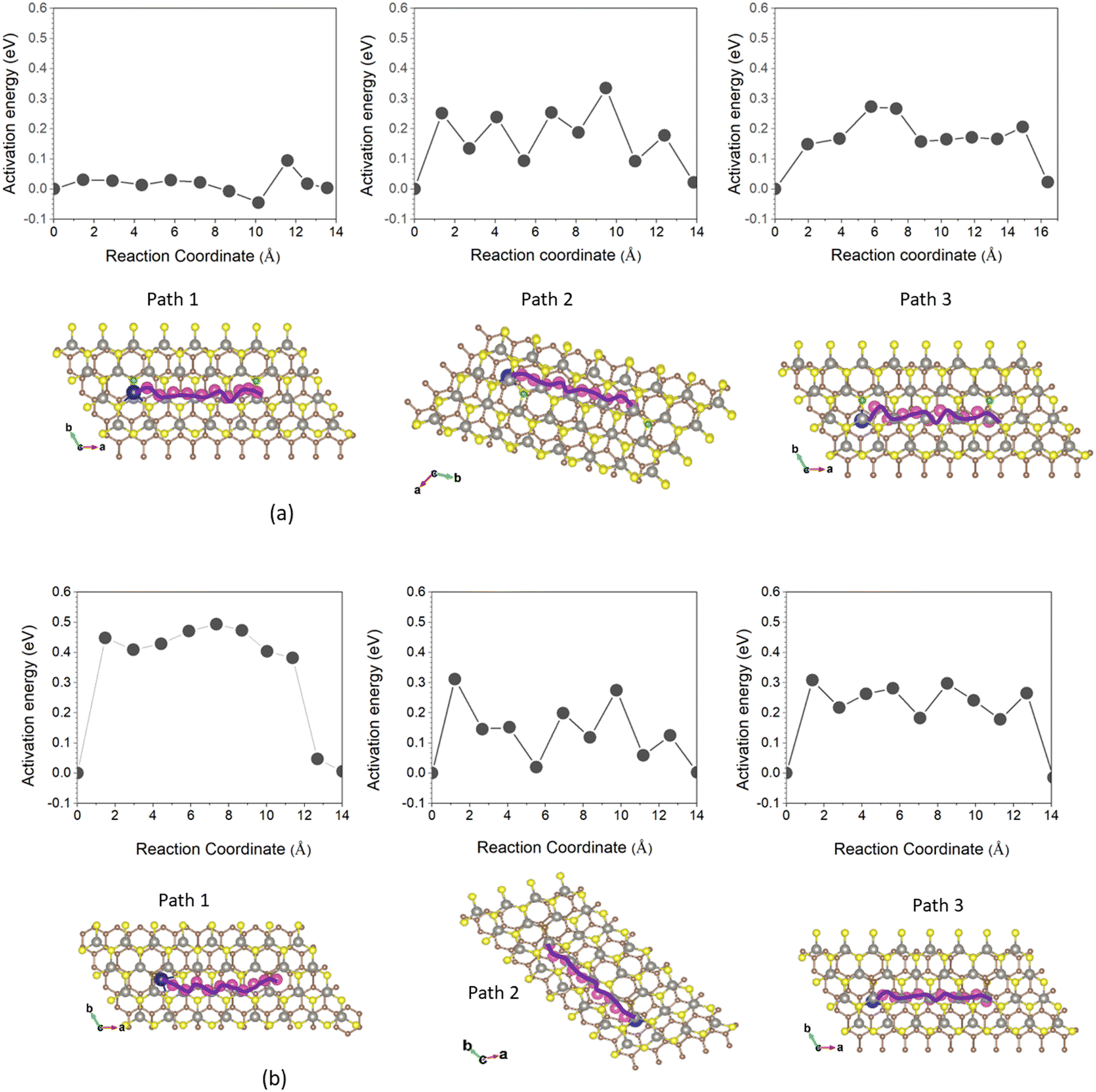 | ||
| Fig. 6 The activation energy profiles (upper images) of Na ions of B-doped WS2/G (a) and C-doped WS2/G (b) of as Na moving along three different diffusion paths (corresponding lower images) indicated by purple curves stacked above purple-colored balls. Path 1 is on the surface along the a-direction, path 2 is in the interface space along the b-direction, and path 3 is in the interface along the a-direction. | ||
Fig. 6 presents the activation energy profiles as a function of the migration coordinate for Na diffusion along the three diffusion paths in both B- and C-doped WS2/G heterostructures. The profiles reveal that the energy barrier for Na migration above the surface of the doped WS2/G strongly depends on the type of dopant. Specifically, the energy barrier for Na diffusion on the surface of C-doped WS2/G is 0.494 eV, which is moderate and comparable to the energy barrier for Na migration through the interface of 1T-MoS2/G11 and Li migration in the interlayer space of WS2/G without doping.17 However, for the B-doped WS2/G system, the energy barrier for Na migration on the surface is considerably smaller, 0.091 eV, which is comparable to that of pristine graphene sheets66 and much smaller than that of pristine TMD nanosheets (0.49–0.95 V).67 This remarkable difference is mainly attributed to the electronegativity of the dopant type. As illustrated in Fig. 3(c), B doping with lower electronegativity compared to S induces carrier delocalization across the WS2 layer within the heterostructure, thereby significantly accelerating Na+ ion transport, as previously reported.68 Conversely, C doping with higher electronegativity results in carrier localization as shown in Fig. 3(e), which leads to a higher of the energy carrier for Na migration. This finding highlights the critical role of dopant selection as a strategic design approach for optimizing Na-ion mobility in WS2/graphene-based anode materials. For Na+ migration through the interfacial region along the a- and b-directions of the B- and C-doped WS2/graphene heterostructures, a slight difference in the activation energy profiles is observed between the two directions, as shown in Fig. 6. The energy barriers fall within a narrow range of 0.274 to 0.335 eV. These values are notably lower than those of pristine TMD nanosheets67 and similar heterostructure such as 1T-MoS2/G (∼0.7 eV),11 facilitating favorable Na+ diffusion within the interfacial space. The low migration barrier of Na ions in the interface region is attributed to two main factors. First, introducing dopants enhances the electrical conductivity of the system with good electrical conductivity of metallic materials, thereby facilitating charge transport.69 Second, introducing dopants breaks the local intrinsic lattice symmetry of heterostructures, which lead to a charge inhomogeneity, creating low potential energy landscape for Na ion immigration at interface region.21 These findings demonstrates that B/C doping in WS2/G heterostructures can create energetically favourable pathway for sodium ions, similar to that pointed out in previous reports.70
Concluding remarks
We investigated the effects of boron (B) and carbon (C) doping on sodium intercalation and diffusion mechanisms in WS2/G heterostructures, aiming to develop advanced anode materials for sodium-ion batteries (SIBs). The electronic structure calculations indicate that doped WS2/G heterostructures exhibit electronic properties of metallic materials. Doping leads to the emergence of additional impurity states, which act as extra energy levels, affecting electronic properties of the systems by allowing more effortless movement of electrons through the material during electrochemical reactions. Notably, substituting surface sulfur atoms with B or C creates chemically active sites that enhance the binding affinity of Na+ ions both on the surface and at interfacial region of the heterostructures. The most stable configurations exhibit strong adsorption energies, with values reaching as low as −1.702 eV, which may effectively suppress sodium dendrite formation during cycling. Climbing-image nudged elastic band calculations show that B/C doping generates low-energy diffusion pathways, with Na+ migration barriers ranging from 0.091 to 0.494 eV, favorable for both surface and interfacial transport. Moreover, the doped WS2/G systems exhibit a small volumetric change upon Na intercalation, making them suitable candidates for developing anodes in batteries with high cycling stability.By analyzing idealized theoretical models, our work uncovers the role of dopants in tailoring sodium intercalation and diffusion processes in WS2/G heterostructures, offering guidance for the design of advanced anode materials. However, translating these theoretical insights into real electrochemical performance under practical cycling conditions requires a further consideration of several key factors such as dopant distribution uniformity, defect formation, and potential Na clustering at high concentrations, which may significantly influence Na intercalation behavior and alter ion diffusion kinetics. This study opens new avenues for future research to bridge the gap between theory and experiment. Promising directions include evaluating the long-term cycling stability of doped WS2/G heterostructures under realistic battery operating conditions, assessing thermal stability and structural integrity during Na intercalation via Ab initio Molecular Dynamics simulations, and investigating long-term ion diffusion and storage kinetics through kinetic Monte Carlo (KMC) methods.
Data availability
The data supporting this article have been included as part of the ESI.†Author contributions
Thi Nhan Tran: writing original draft, review & editing, validation, conceptualization, data curation, formal analysis, investigation, methodology. Nguyen Hoang Son: data curation, formal analysis. Nguyen Minh Hieu: data curation, formal analysis. Yoshiyuki Kawazoe: software, supervision. Luong Huu Duc: formal analysis, review & editing supervision. Thuy Trang Nguyen: writing original draft, investigation, conceptualization, data curation, formal analysis. Minh Triet Dang: writing – review & editing, investigation, methodology, conceptualization. Phi Long Nguyen: formal analysis, investigation. Viet Bac Phung Thi: review & editing, formal analysis, investigation, funding acquisition, resources, software.Conflicts of interest
There are no conflicts to declare.Acknowledgements
The authors acknowledge the support provided by the VinUniversity Center for Environmental Intelligence under Flagship Projects VUNI.CEI.FS_0005.References
- M. Wakihara, Recent developments in lithium-ion batteries, Mater. Sci. Eng., R, 2001, 33(4), 109–134, DOI:10.1016/S0927-796X(01)00030-4.
- R. Fang, S. Zhao, Z. Sun, D. W. Wang, H. M. Cheng and F. Li, More reliable lithium-sulfur batteries: status, solutions and prospects, Adv. Mater., 2017, 29(48), 1606823, DOI:10.1002/ADMA.201606823.
- S. Peng, X. Kong, J. Li, J. Zeng and J. Zhao, Alleviating the storage instability of LiNi0.8Co0.1Mn0.1O2 cathode materials by surface modification with poly(acrylic acid), ACS Sustain. Chem. Eng., 2021, 9(22), 7466–7478, DOI:10.1021/acssuschemeng.1c00802.
- M. S. Balogun, Y. Luo, W. Qiu, P. Liu and Y. Tong, A review of carbon materials and their composites with alloy metals for sodium ion battery anodes, Carbon N Y, 2016, 98, 162–178, DOI:10.1016/J.CARBON.2015.09.091.
- M. Mamoor, et al., Recent progress on advanced high energy electrode materials for sodium ion batteries, Green Energy and Resources, 2023, 1(3), 100033, DOI:10.1016/J.GERR.2023.100033.
- S. Ghosh, Z. Qi, H. Wang, S. K. Martha and V. G. Pol, WS2 anode in Na and K-ion battery: effect of upper cut-off potential on electrochemical performance, Electrochim. Acta, 2021, 383, 138339, DOI:10.1016/J.ELECTACTA.2021.138339.
- B. Kang, et al., Facile fabrication of WS2 nanocrystals confined in chlorella-derived N, P co-doped bio-carbon for sodium-ion batteries with ultra-long lifespan, Dalton Trans., 2021, 50(41), 14745–14752, 10.1039/D1DT01582F.
- M. Latha and J. V. Rani, WS2/graphene composite as cathode for rechargeable aluminum-dual ion battery, J. Electrochem. Soc., 2020, 167(7), 70501, DOI:10.1149/2.0012007JES/XML.
- R. Raccichini, A. Varzi, S. Passerini and B. Scrosati, The role of graphene for electrochemical energy storage, Nat. Mater., 2014, 14(3), 271–279, DOI:10.1038/nmat4170.
- L. Ji, P. Meduri, V. Agubra, X. Xiao and M. Alcoutlabi, Graphene-based nanocomposites for energy storage, Adv. Energy Mater., 2016, 6(16), 1502159, DOI:10.1002/AENM.201502159.
- A. Massaro, A. Pecoraro, A. B. Muñoz-García and M. Pavone, First-principles study of Na intercalation and diffusion mechanisms at 2D MoS2/graphene interfaces, J. Phys. Chem. C, 2021, 125(4), 2276–2286, DOI:10.1021/acs.jpcc.0c10107.
- D. Su, S. Dou and G. Wang, WS2@graphene nanocomposites as anode materials for Na-ion batteries with enhanced electrochemical performances, Chem. Commun., 2014, 50(32), 4192–4195, 10.1039/C4CC00840E.
- Z. Yuan, Q. Jiang, C. Feng, X. Chen and Z. Guo, Synthesis and performance of tungsten disulfide/carbon (WS2/C) composite as anode material, J. Electron. Mater., 2018, 47(1), 251–260, DOI:10.1007/S11664-017-5740-1/METRICS.
- A. Rossi, H. Büch, C. D. Rienzo, V. Miseikis, D. Convertino, A. Al-Temimy, V. Voliani, M. Gemmi, V. Piazza and C. Coletti, Scalable synthesis of WS2 on graphene and h-BN: an all-2D platform for light-matter transduction, 2D Mater, 2016, 3(3), 031013, DOI:10.1088/2053-1583/3/3/031013.
- H. Li, K. Yu, H. Fu, B. Guo, X. Lei and Z. Zhu, Multi-slice nanostructured WS2@rGO with enhanced Li-ion battery performance and a comprehensive mechanistic investigation, Phys. Chem. Chem. Phys., 2015, 17(44), 29824–29833, 10.1039/C5CP04081G.
- R. Chen, et al., Free-standing hierarchically sandwich-type tungsten disulfide nanotubes/graphene anode for lithium-ion batteries, Nano Lett., 2014, 14(10), 5899–5904, DOI:10.1021/nl502848z.
- T. K. Bijoy, S. Sudhakaran and S. C. Lee, WS2-graphene van der Waals heterostructure as promising anode material for lithium-ion batteries: a first-principles approach, ACS Omega, 2024, 9(6), 6482–6491, DOI:10.1021/acsomega.3c06559.
- N. Choudhary, M. A. Islam, J. H. Kim, T. J. Ko, A. Schropp, L. Hurtado, D. Weitzman, L. Zhai and Y. Jung, wo-dimensional transition metal dichalcogenide hybrid materials for energy applications, Nano Today, 2018, 19, 16–40, DOI:10.1016/j.nantod.2018.02.007.
- D. Kong, X. Qiu, B. Wang, Z. Xiao, X. Zhang, R. Guo, Y. Gao, Q.-H. Yang and L. Zhi, ‘S2 nanoplates embedded in graphitic carbon nanotubes with excellent electrochemical performance for lithium and sodium storage, Sci. China Mater., 2018, 61(5), 671–678, DOI:10.1007/s40843-017-9185-3.
- T. Li, R. Guo, Y. Luo, F. Li, L. Meng, X. Sun, Z. Yang, H. Luo and Y. Wan, Improved lithium and sodium ion storage properties of WS2 anode with three-layer shell structure’, Electrochim. Acta, 2020, 331, 135424, DOI:10.1016/j.electacta.
- M. Han, Y. Mu, Y. Cai, L. Wei, L. Zeng and T. Zhao, Atomic-interface strategy and N,O co-doping enable WS2 electrodes with ultrafast ion transport rate in sodium-ion batteries, J. Mater. Chem. A, 2022, 10, 20283–20293, 10.1039/D2TA04984H.
- S. H. Woo, et al, Fullerene-like Re-doped MoS2 nanoparticles as an intercalation host with fast kinetics for sodium ion batteries, Isr. J. Chem., 2015, 55(5), 599–603, DOI:10.1002/IJCH.201400124.
- M. Qin, et al, K intercalation-assisted Co-doped MoS2 nanoflowers for an efficient hydrogen evolution reaction, Precis. Chem., 2023, 1(8), 497–506, DOI:10.1021/prechem.3c00033.
- T. K. C. Phu, et al., Spent zinc-carbon battery-derived carbon nanoparticles coupled with transition metal dichalcogenides for enhanced pH-universal hydrogen evolution reaction, ACS Appl. Energy Mater., 2024, 7(23), 10938–10949, DOI:10.1021/acsaem.4c01791.
- S. Wang, et al., ‘Synthesis and characterization of cobalt-doped WS2 nanorods for lithium battery applications’, Nanoscale Res. Lett., 2010, 5(8), 1301–1306, DOI:10.1007/S11671-010-9642-X/FIGURES/6.
- G. Kresse and J. Furthmüller, Efficient iterative schemes for ab initio total-energy calculations using a plane-wave basis set, Phys. Rev. B: Condens. Matter Mater. Phys., 1996, 54(16), 11169, DOI:10.1103/PhysRevB.54.11169.
- G. Kresse and J. Furthmüller, Efficiency of ab initio total energy calculations for metals and semiconductors using a plane-wave basis set, Comput. Mater. Sci., 1996, 6(1), 15–50, DOI:10.1016/0927-0256(96)00008-0.
- J. P. Perdew, K. Burke and M. Ernzerhof, Generalized gradient approximation made simple, Phys. Rev. Lett., 1996, 77(18), 3865, DOI:10.1103/PhysRevLett.77.3865.
- J. Klime, D. R. Bowler and A. Michaelides, Van der Waals density functionals applied to solids, Phys. Rev. B:Condens. Matter Mater. Phys., 2011, 83(19), 195131, DOI:10.1103/PHYSREVB.83.195131/FIGURES/7/THUMBNAIL.
- H. J. Monkhorst and J. D. Pack, Special points for Brillouin-zone integrations, Phys. Rev. B: Condens. Matter Mater. Phys., 1976, 13(12), 5188–5192, DOI:10.1103/PhysRevB.13.5188.
- V. Wang, N. Xu, J. C. Liu, G. Tang and W. T. Geng, VASPKIT: A user-friendly interface facilitating high-throughput computing and analysis using VASP code, Comput. Phys. Commun., 2021, 267, 108033, DOI:10.1016/J.CPC.2021.108033.
- W. Tang, E. Sanville and G. Henkelman, A grid-based Bader analysis algorithm without lattice bias, J. Phys.: Condens. Matter, 2009, 21(8), 084204, DOI:10.1088/0953-8984/21/8/084204.
- G. Henkelman, B. P. Uberuaga and H. Jónsson, A climbing image nudged elastic band method for finding saddle points and minimum energy paths, J. Chem. Phys., 2000, 113(22), 9901–9904, DOI:10.1063/1.1329672.
- G. Henkelman and H. Jónsson, Improved tangent estimate in the nudged elastic band method for finding minimum energy paths and saddle points, J. Chem. Phys., 2000, 113(22), 9978–9985, DOI:10.1063/1.1323224.
- Z. Ghasemi majd, P. Amiri and S. F. Taghizadeh, Ab-initio study of structural and electronic properties of WS2/h-BN van der Waals heterostructure, Surf. Sci., 2018, 672–673, 13–18, DOI:10.1016/j.susc.2018.03.00.
- Q. H. Tran, T. N. Tran, T. T. Luong, V. T. Ngo, V. B. T. Phung and V. A. Dinh, Band valley flattening and exciton appearance/disappearance under isotropic strain in monolayer WS2, Eur. Phys. J. Plus, 2022, 137(12), 1–11, DOI:10.1140/EPJP/S13360-022-03537-2.
- V. B. T. Phung, T. N. Tran, Q. H. Tran, T. T. Luong and V. A. Dinh, Graphene as a Sensor for Lung Cancer: Insights into Adsorption of VOCs Using vdW DFT, ACS Omega, 2024, 9(2), 2302–2313, DOI:10.1021/acsomega.3c06159.
- A. Jorio, et. al., Stokes and anti-Stokes Raman spectra of the high-energy C–C stretching modes in graphene and diamond, Phys. Status Solidi B, 2015, 252(11), 2380–2384, DOI:10.1002/pssb.201552224.
- V. B. T. Phung, et al., First-principles study of highly sensitive graphene/hexagonal boron nitride heterostructures for application in toxic gas-sensing devices, RSC Adv., 2024, 14(7), 4904–4916, 10.1039/D3RA08017J.
- J. Kang, J. Li, S. S. Li, J. B. Xia and L. W. Wang, Electronic structural Moiré pattern effects on MoS2/MoSe2 2D heterostructures, Nano Lett., 2013, 13(11), 5485–5490, DOI:10.1021/nl4030648.
- Y. Gao, Q. Liu and B. Xu, Lattice mismatch dominant yet mechanically tunable thermal conductivity in bilayer heterostructures, ACS Nano, 2016, 10(5), 5431–5439, DOI:10.1021/acsnano.6b01674.
- I. Leven, T. Maaravi, I. Azuri, L. Kronik and O. Hod, Interlayer potential for graphene/h-BN heterostructures, J. Chem. Theory Comput., 2016, 12(6), 2896–2905, DOI:10.1021/ACS.JCTC.6B00147.
- S. Singh, C. Espejo and A. H. Romero, Structural, electronic, vibrational, and elastic properties of graphene/MoS2 bilayer heterostructures, Phys. Rev. B, 2018, 98(15), 155309, DOI:10.1103/PhysRevB.98.155309.
- M. Zhang, C. Tang, W. Cheng and L. Fu, The first-principles study on the performance of the graphene/WS2 heterostructure as an anode material of Li-ion battery, J. Alloys Compd., 2021, 855, 157432, DOI:10.1016/J.JALLCOM.2020.157432.
- S. Deng, L. Li and P. Rees, Graphene/MoXY Heterostructures Adjusted by Interlayer Distance, External Electric Field, and Strain for Tunable Devices, ACS Appl. Nano Mater., 2019, 2(6), 3977–3988, DOI:10.1021/acsanm.9b00871.
- D. Pierucci, et al, Band alignment and minigaps in monolayer MoS2-graphene van der Waals heterostructures, Nano Lett., 2016, 16(7), 4054–4061, DOI:10.1021/acs.nanolett.6b00609.
- S. Fu, Z. Ma, Z. Huang, X. Zhu, M. Yan and Y. Fu, The first-principles study on the graphene/MoS2 heterojunction, AIP Adv., 2020, 10, 045225, DOI:10.1063/1.5144078.
- J. Yang, X. Zhou, D. Wu, X. Zhao and Z. Zhou, S-Doped N-Rich Carbon Nanosheets with Expanded Interlayer Distance as Anode Materials for Sodium-Ion Batteries, Adv. Mater., 2017, 29(6), 1604108, DOI:10.1002/adma.201604108.
- R. Kumar, A. K. Shringi, H. J. Wood, I. M. Asuo, S. Oturak, D. E. Sanchez, T. K. Sharma, R. Chaurasiya, W. M. Choi, N. Y. Doumon and M. Terrones, Substitutional doping of 2D transition metal dichalcogenides for device applications: Current status, challenges and prospects, Mater. Sci. Eng, R, 2025, 154, 100946, DOI:10.1016/j.mser.2025.100946.
- Y. Xia, L.-F. Que, F.-D. Yu, L. Deng, C. Liu, X.-L. Sui, L. Zhao and Z.-B. Wang, Boosting ion/e- transfer of Ti3C2 via interlayered and interfacial co-modification for high-performance Li-ion capacitors’, Chem. Eng. J., 2021, 404, 127116, DOI:10.1016/j.cej.2020.127116.
- M. Ma, N. Lu, F. Ling, J. Dai, J. Jiang, R. Bai, Z. Li, Z. Zhuo, Y. Shao, Y. Yao, H. Huo and Y. Yu, Interface Engineering with ZrS2: Achieving 10000-Cycle Lifespan in High-Rate Sodium Metal Batteries, Adv. Energy Mater., 2025, 15, 2502416, DOI:10.1002/aenm.202502416.
- H. Yang, W. Liang, X. Guo, C. M. Wang and S. Zhang, Strong kinetics–stress coupling in lithiation of Si and Ge anodes, Extreme Mechanics Letters, 2015, 2(1), 1–6, DOI:10.1016/j.eml.2014.11.008.
- S. Zhang, K. Zhao, T. Zhu and J. Li, Electrochemo mechanical degradation of high-capacity battery electrode materials, Prog. Mater. Sci., 2017, 89, 479–521, DOI:10.1016/j.pmatsci.2017.04.014.
- J. Luo, et al., In situ measurements of mechanical and volume change of LiCoO2 lithium-ion batteries during repeated charge–discharge cycling by using digital image correlation, Measurement, 2016, 94, 759–770, DOI:10.1016/J.MEASUREMENT.2016.09.023.
- M. Woodcox, R. Shepard and M. Smeu, First principles investigation into the interwoven nature of voltage and mechanical properties of the LixNMC-811 cathode, J. Power Sources, 2021, 516, 230620, DOI:10.1016/J.JPOWSOUR.2021.230620.
- S. Schweidler, L. De Biasi, A. Schiele, P. Hartmann, T. Brezesinski and J. Janek, Volume changes of graphite anodes revisited: a combined operando x-ray diffraction and in situ pressure analysis study, J. Phys. Chem. C, 2018, 122(16), 8829–8835, DOI:10.1021/ACS.JPCC.8B01873.
- Q. Wei, M. Gao, Y. Li, D. Zhang, S. Wu, Z. Chen and Y. Sun, Directionally assembled MoS2 with significantly expanded interlayer spacing: a superior anode material for high-rate lithium-ion batteries, Mater. Chem. Front., 2018, 2(8), 1441–1448, 10.1039/C8QM00117K.
- Z. Hu, X. Liu, P. L. Hernández-Martínez, S. Zhang, P. Gu, W. Du, W. Xu, H. V. Demir, H. Liu and Q. Xiong, Interfacial charge and energy transfer in van der Waals heterojunctions, InfoMat, 2022, 4(3), e12290, DOI:10.1002/inf2.12290.
- T. P. Kaloni, L. Kou, T. Frauenheim and U. Schwingenschlögl, Quantum spin Hall states in graphene interacting with WS2 or WSe2, Appl. Phys. Lett., 2014, 105(23), 233112, DOI:10.1063/1.4903895.
- E. Moradpur-Tari, R. Sarraf-Mamoory and A. Yourdkhani, Structural, electronic, and electrochemical studies of WS2 phases using density functional theory and machine learning, Phys. B, 2023, 650, 414568, DOI:10.1016/j.physb.2022.414568.
- J. Park, M. S. Kim, E. Cha, J. Kim and W. Choi, Synthesis of uniform single layer WS2 for tunable photoluminescence, Sci. Rep., 2017, 7(1), 1–8, DOI:10.1038/s41598-017-16251-2.
- S. Aeschlimann, A. Rossi, M. Chavez-Cervantes, R. Krause, B. Arnoldi, B. Stadtmüller, M. Aeschlimann, S. Forti, F. Fabbri, C. Coletti and I. Gierz, Direct evidence for efficient ultrafast charge separation in epitaxial WS2/graphene heterostructures, Sci. Adv., 2020, 6(20), eaay0761, DOI:10.1126/sciadv.aay0761.
- Q. Liu, W. Xia, Z. Wu, J. Huo, D. Liu, Q. Wang and S. Wang, The origin of the enhanced performance of nitrogen-doped MoS2 in lithium-ion batteries, Nanotechnology, 2016, 27(17), 175402, DOI:10.1088/0957-4484/27/17/175402.
- B.-N. Yun, H. L. Du, J.-Y. Hwang, H.-G. Jung and Y.-K. Sun, Improved electrochemical performance of boron-doped carbon-coated lithium titanate as an anode material for sodium-ion batteries, J. Mater. Chem. A, 2017, 5(6), 2802–2810, 10.1039/C6TA10494K.
- K. Guan, Y. Li, L. Liu, F. Sun, Y. Wang, Z. Zheng, W. Zhou, C. Zhang, Z. Cai, X. Wang, S. Feng and T. Zhang, Atomic Nb-doping of WS2 for high-performance synaptic transistors in neuromorphic computing, Microsyst. Nanoeng., 2024, 10, 132, DOI:10.1038/s41378-024-00779-1.
- E. Olsson, G. Chai, M. Dove and Q. Cai, Adsorption and migration of alkali metals (Li, Na, and K) on pristine and defective graphene surfaces, Nanoscale, 2019, 11(12), 5274–5284, 10.1039/C8NR10383F.
- E. Yang, H. Ji and Y. Jung, Two-Dimensional Transition Metal Dichalcogenide Monolayers as Promising Sodium Ion Battery Anodes, J. Phys. Chem. C, 2015, 119(47), 26374–26380, DOI:10.1021/acs.jpcc.5b09935.
- (a) H. Yu, Y. Gao, H. Jing, J. Wang, Q. Liang, J. Kang, X. Wang, C.-F. Du and X. Wu, Boron-Doping Induced Electron Delocalization in Fluorophosphate Cathode: Enhanced Na-Ion Diffusivity and Sodium-Ion Full Cell Performance, Small, 2023, 19(39), 2302097, DOI:10.1002/smll.202302097; (b) S. Bagheri, M. Nasrollahpour and M. Vafaee, Investigating the Structure, Electronic Properties, and Ion Migration of Na3V2(PO4)3 Cathodes via Mono/Multi-Element Doping of Cr, Fe, and Si: A First-Principles Study, ACS Omega, 2023, 8(12), 11035–11044, DOI:10.1021/acsomega.2c07952.
- S. Bagheri, M. Nasrollahpour and M. Vafaee, Investigating the Structure, Electronic Properties, and Ion Migration of Na3V2(PO4)3 Cathodes via Mono/Multi-Element Doping of Cr, Fe, and Si: A First-Principles Study, ACS Omega, 2023, 8(12), 11035–11044, DOI:10.1021/acsomega.2c07952.
- S. G. Shirazi, M. Nasrollahpour and M. Vafaee, Investigation of Boron-Doped Graphdiyne as a Promising Anode Material for Sodium-Ion Batteries: A Computational Study, ACS Omega, 2020, 5(17), 10034–10041, DOI:10.1021/acsomega.0c00422.
Footnote |
| † Electronic supplementary information (ESI) available. See DOI: https://doi.org/10.1039/d5ra04616e |
| This journal is © The Royal Society of Chemistry 2025 |