
 Open Access Article
 This Open Access Article is licensed under a
 Creative Commons Attribution 3.0 Unported Licence
Thermally evaporated Cu2−xSe thin films embedded with PbSe nanoinclusions: a multiphase system for thermoelectric applications
Ammara Shakoora,
Sajid Butt *a,
Muhammad Faizan Masouda,
Muhammad Umer Iqbalb and
Muhammad Yasirc
*a,
Muhammad Faizan Masouda,
Muhammad Umer Iqbalb and
Muhammad Yasirc
aDepartment of Space Science, Institute of Space Technology, Islamabad 44000, Pakistan. E-mail: sajid.butt@ist.edu.pk
bCentre for Functional and Surface Functionalized Glass, Alexander Dubcek University of Trencin, Slovakia
cDepartment of Material Science & Engineering, Institute of Space Technology, Islamabad, 44000, Pakistan
First published on 14th July 2025
Abstract
Thermoelectric (TE) devices pave a promising pathway for clean and efficient energy conversion between heat and electricity. Among various TE materials, copper selenide (Cu2Se) has attracted significant interest due to its high electrical conductivity and low thermal conductivity offered by its superionic behavior, making it a candidate for high-performance thermoelectric applications. The present study systematically investigates the TE properties of thin film-based nanocomposites comprised of lead (Pb)-doped Cu(2−x)Se integrated with lead selenide (PbSe) samples. XPS analysis infers the incorporation of Pb and reveals changes in the oxidation states and bonding environments of Cu and Se. Thermoelectric measurements in the temperature range of 300 K to 400 K demonstrate that Pb incorporation influences charge carrier transportation, as inferred alteration in the Seebeck coefficient and electrical conductivity. A slightly overestimated value of the figure-of-merit (ZT) has been evaluated by merely relying on the electronic thermal conductivity (ke) and ignoring the lattice thermal conductivity (κl). This work reveals the importance of multiphase compositions in tuning of TE properties and suggests a route for deeper understanding of transport mechanisms in thin film samples.
Introduction
Thermoelectric (TE) devices are gaining immense importance because of their utility in clean and efficient conversion between heat and electricity for sustainable energy solutions. The TE devices, having no moving parts, zero emissions, and without acoustic noise, offer an environmentally friendly solution for electricity generation and solid-state refrigeration by efficiently recycling waste heat being released from industry and automobiles.1 They find applications in diverse areas such as automotive seat temperature regulation, industrial waste heat utilization, and low-power wearable or implantable biomedical devices.2 The TE performance of a material is determined by its ability to convert heat into electrical energy and vice versa. This performance depends on the material's intrinsic properties, typically characterized by the Seebeck coefficient (S), electrical conductivity (σ), and thermal conductivity (κ), as connected by a dimensionless figure of merit: , where T the absolute temperature. High-performance (TE) materials are typically characterized by a high power factor (PF) and low thermal conductivity (κ), as tailored by tuning of carrier concentration.3,4 To enhance ZT, several strategies have been adopting including; introducing resonant energy levels or carrier filtering effects,5 band structure engineering,6,7 optimizing carrier concentration through elemental doping,8–10 bulk-nano compositing,11–13 grain-texturing,14–16 and reduction of lattice thermal conductivity by incorporation of rattling atoms.17
In the last two decades, various classes of materials such as chalcogenides,18,19 clathrates,20 skutterudites21 and oxides7,22 have undergone extensive investigation in search of efficient TE materials. While oxide-based TE materials traditionally exhibit relatively low (ZT) values, which limits their commercial viability, they receive growing attention due to their cost-effectiveness and exceptional thermal stability at elevated temperatures.23 Amongst chalcogenides, Cu(2−x)S has been extensively explored due to its large electrical conductivity and low thermal conductivity offered by superionic behavior.23,24 Below 400 K, Cu(2−x)S crystalizes in numerous crystalline phases such as cubic,25,26 tetragonal,27,28 orthorhombic,29,30 monoclinic,31,32 and hexagonal.33 Around 400 K, Cu(2−x)Se undergoes a solid-state phase transition from the low-temperature α-phase to the high-temperature β-phase (cubic only). In both phases, selenium (Se) atoms occupy face-centered cubic (FCC) sites. However, copper (Cu) atoms exhibit distinct behaviors in the α-phase, Cu atoms are well-ordered and confined, whereas in the β-phase, they become kinetically disordered and display superionic conduction behavior.34,35 The diverse physical, chemical, and thermal characteristics of copper selenide and its related compounds are caused by variations in composition and crystallography.36 Due to the wide range of accessible crystal structures, tunable particle sizes, and compatible band gaps, copper selenide materials exhibit intriguing optoelectronic properties that can be finely tailored for specific applications. Cu2Se exhibits a moderate Seebeck coefficient, low thermal and high electrical conductivity. According to the literature, Cu2Se synthesized via melting followed by spark plasma sintering (SPS) achieves a significant figure of merit (ZT) of 1.5 at 1000 K, demonstrating its potential for high-temperature thermoelectric applications.37 Doping tellurium (Te) at the selenium site enabled Cu2Se to have a higher ZT value of 1.9 at 873 K.38 Using S-doped Cu2Se, (ZT) was further improved up to 2.0 at 1000 K.39 Currently, the Al-doped Cu2Se bulk has the greatest (ZT) value, 2.62 at 1029 K.40 Extensive research has been conducted on doping Cu2Se to enhance its thermoelectric (TE) performance, with numerous studies confirming that dopants significantly influence the material's (TE) properties. For instance, incorporating aluminum (Al) can modify the microstructure of Cu2Se, thereby affecting its thermoelectric behavior. At 1029 K, the highest (ZT) value recorded for Al-doped Cu2Se bulk materials is 2.62. A variety of dopants, spanning across all major groups as well as several transition elements, have been explored for doping Cu2Se. Qiujun Hu et al. synthesized Li-doped Cu1.98Li0.02Se bulk materials using hydrothermal synthesis followed by hot pressing, achieving a high (ZT) value of 2.14 at 973 K.41 Zhao et al. have carried out extensive studies on Cu2Se doped by a range of carbon resources, including graphite (G), carbon nanotubes (CNT), super P (SP), and hard carbon (H). The greatest (ZT) value of 2.4 at 850 K was obtained by 0.3 weight percent carbon fiber-doped Cu2Se. Melt quenching and solid-state reactions are used to create the composites.42,43 Moreover, Zhu et al. produced a Pb-doped Cu2Se material with the same layered structure.44 They discovered in their experiments that the thermal conductivity decreases with the lamellae width and grain boundaries effectively disperse phonons and carriers.
Although bulk Cu2Se exhibits superior thermoelectric (TE) performance compared to its thin film counterparts, but Cu2Se thin films offer distinct advantages like reducing materials consumption. In addition to reducing material consumption and associated costs, thin films are particularly suitable for device miniaturization and integration into microscale systems. Various deposition techniques for Cu(2−x)Se thin films have been reported in the literature, including solution,39,45 electrodeposition,46 pulsed laser deposition,47 ion beam sputtering deposition,48 reactive evaporation,49 and pulsed/magnetron sputtering.50
In this work, the thermoelectric transport properties of Pb-doped Cu(2−x)Se thin films have been systematically explored and explained with the help of detailed structural characterizations. Comparing vacuum thermal evaporation to other thin film deposition techniques, it offers several benefits, including consistent film thickness, good compaction, and adhesion to glass substrate. It is also readily available.
Experimentation
Preparation of thin films
The complete synthesis and characterization procedure is illustrated in Fig. 1. A series of thin films, including pristine Cu2Se and lead-doped variants Cu2Se0.95Pb0.05 (Pb-5%), Cu2Se0.9Pb0.1 (Pb-10%), Cu2Se0.75Pb0.25 (Pb-25%), Cu2Se0.5Pb0.5 (Pb-50%), and Cu2Se0.25Pb0.75 (Pb-75%) were synthesized via thermal evaporation technique. For all the series, films having a thickness of 500 nm were deposited over a pre-cleaned glass substrate, using Nanovak NVBJ-300 TH thermal evaporator equipped with a tungsten boat. The chamber was evacuated to a pressure of 5.0 × 10⁻⁶ mbar before deposition. A current in the range of 90–100 A was applied to achieve a stable deposition rate of 0.5 Å s−1. The as-deposited films were annealed at 400 °C for 1 hour to in an inert atmosphere. | ||
| Fig. 1 Schematic diagram of revealing the fabrication and structural and thermoelectric characterization of pristine and Pb-doped Cu2−xSe thin films. | ||
Characterization
X-ray diffraction (XRD) patterns were obtained using BRUKER diffractometer (D2 PHASER) equipped with Cu-Kα radiations (λ ∼1.54 Å). XPS (X-ray Photoelectron Spectroscopy), a surface-sensitive analytical technique, was used to determine chemical states of all the elements. The high-resolution spectra of Cu2p, Se3d, and Pb4f were deconvoluted using XPSPEAK41 software. A Scanning Electron Microscopy (SEM) model (ZEISS Gemini 300-8202017309) was used to study surface morphology and phase distribution of all the pristine and Pb-doped Cu2Se-based thin films using secondary electrons (SE) and backscattered electrons (BSE), respectively. The particle size distribution was estimated from SEM images using IMAGEJ software. The qualitative and quantitative elemental composition was determined using energy dispersive X-ray spectroscopy (EDS), as equipped with SEM. The electrical conductivity and Seebeck coefficient were measured for the α-phase over a temperature range of 300–400 K, using the four-probe geometry with a Thermoelectric Parameter Testing System (Joule-Yacht-Namicro-3L).Results and discussion
Fig. 2 shows the X-ray diffraction (XRD) patterns of powdered Cu(2−x)Se recorded at room temperature. The powder sample exhibits well-defined diffraction peaks corresponding to monoclinic and cubic polymorphs, as indexed by PDF# 27-1131 and PDF# PDF#06-0680, respectively.23,51 In contrast, the XRD patterns of the Cu(2−x)Se thin films display no distinct diffraction peaks. Instead, a broad amorphous hump was observed, which originates from the glass substrate on which the films were deposited. As a result, structural analysis of the thin films using XRD was not feasible. Therefore, X-ray photoelectron spectroscopy (XPS) was employed to investigate the composition and chemical states of the elements present in the films. | ||
| Fig. 2 Room temperature XRD pattern of the bulk Cu(2−x)Se sample employed for thin film deposition. | ||
The XPS full survey spectra of pristine Cu(2−x)Se and Pb-5% doped Cu(2−x)Se thin films are shown in Fig. 3(a). The presence of Cu, Se, and Pb is confirmed by the respective core-level binding energies. C 1s peak located near 284.8 eV can be seen clearly, which serves the purpose of reference for charge correction.52 Fig. 3(b) presents the high-resolution Cu 2p spectrum. The peaks corresponding to Cu+ and Cu2+ oxidation states confirm the mixed valence nature of copper, which is characteristic of the non-stoichiometric phase and superionic behavior of Cu(2−x)Se.12 The slight shift in Cu1+ binding energy suggests changes in the local bonding environment, which is in good agreement with that of the previously reported data on pure and doped Cu(2−x)Se.23,51,53 However, the Cu–O component indicates surface oxidation or interaction with residual oxygen. The Se 3d core-level spectrum in Fig. 3(c) shows two well-resolved peaks at ∼54.2 eV and ∼55.2 eV, assigned to Se 3d5/2 and Se 3d3/2 which are spin–orbit split components, respectively. Peaks attributed to Se–Cu bonding confirm the selenide phase, while additional Se–O components suggest partial surface oxidation of selenium.
 | ||
| Fig. 3 XPS analysis of Cu2Se and Pb-5% doped Cu(2−x)Se thin films, (a) full survey spectra showing elemental peaks. (b, e) Cu 2p spectra, (c, f) Se 3d spectra (d) Pb 4f spectrum for pristine and Pb-doped Cu(2−x)Se thin films. | ||
Fig. 3(d) displays the Pb 4f spectrum, where Pb 4f7/2 and Pb 4f5/2 peaks confirm the presence of Pb2+ species. The deconvolution reveals Pb–Se bonds, indicating the formation of PbSe, as well as minor contributions from Pb–O, likely due to surface oxidation. The appearance of Pb–Cu interactions indicates the partial substitution of Pb at the Cu site. In the Cu 2p spectrum for the Pb-doped sample, Fig. 3(e), changes in peak intensity and satellite structure are observed. A reduction in Cu2+ satellite intensity may indicate partial reduction to Cu+, possibly influenced by Pb doping as a result of charge redistribution. The presence of Cu–Pb bonds further supports electronic interactions between Cu and Pb, indicating the partial substitution of Pb at Cu-site. Fig. 3(f) shows the Se 3d spectrum of the Pb-doped sample. Se–Pb bonding suggests the formation of PbSe phases. A noticeable decrease in the Se–Cu component and the persistence of Se–O indicates the redistribution of selenium atoms for the formation of PbSe phase. A slight shift in Se 3d binding energies compared to that of the pristine Cu(2−x)Se sample may reflect electronic structure modification due to Pb incorporation.
Fig. 4(a) presents the SEM image, revealing a relatively uniform distribution of grains with some degree of agglomeration and minor voids. The magnified image indicates a nanocrystalline structure with a clear particle size and shape, as shown in the inset of Fig. 4(a). The particle size distribution, showing an average particle size of approximately 25 nm, in Fig. 4(c) is consistent with a fine-grained nanostructure that can enhance phonon scattering in thermoelectric applications. EDS analysis confirms the presence of Cu and Se elements in the pristine film, affirming the successful deposition of the desired phase, as shown in Fig. 4(b).
 | ||
| Fig. 4 Surface morphology and compositional analysis of Cu2−xSe thin film. (a) FESEM image showing uniform nanoparticle distribution, with an image in the inset showing clear particle size with a range nearly equal to 100 nm. (b) EDS spectrum confirming the presence of Cu and Se elements in pristine Cu2−xSe thin films. (c) Average particle size ∼25 nm. | ||
Fig. 5(a) presents the SEM and elemental concentration analysis of Pb-doped 5% in Cu2Se thin films. The secondary electron (SE) SEM image reveals the surface morphology, showing a granular structure. (Pb) particles appear prominently on the surface, while Cu2Se particles are distributed in the background. In Fig. 5(b), the backscattered electron (BSD) image highlights compositional contrast; brighter regions represent the PbSe inclusions, while darker regions indicate areas containing Cu(2−x)Se matrix. The EDS spectrum confirms the presence of Cu, Se, and Pb in the Pb-doped sample, as shown in Fig. 5(c). The combined XPS, SEM and EDS results confirm the formation of a multiphase system consisting of Cu(2−x)Se matrix embedded with PbSe inclusions.
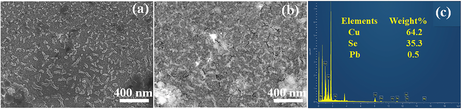 | ||
| Fig. 5 (a) Secondary electron (SE) image, (b) backscattered electron (BSE) image, and (c) elemental composition (EDS)of Cu2Se0.95Pb0.05 (Pb-5%) sample. | ||
The temperature dependent electrical conductivity (σ) and Seebeck coefficient (S) were measured in the temperature range of 300 K to 400 K.
(TE) temperature-dependent parameters, electrical conductivity, Seebeck coefficient, and power factor (PF) for all samples are summarized in Fig. 6. Among the doped series, the Pb-5% sample exhibits the highest electrical conductivity, approximately 5.0 × 10⁴ S m−1, whereas the pristine Cu2Se sample maintains the highest overall conductivity, as illustrated in Fig. 6(a). It can be seen that the electrical conductivity of all the doped series has decreased as compared to the pristine Cu(2−x)Se sample. This decrease is associated with the incorporation of a small amount of Pb into the Cu(2−x)Se lattice introduces point defects that act as scattering centers, thereby reducing the electrical conductivity across all doped series, i.e., 10%, 50%, and 75%. Furthermore, excess Pb leads to the formation of a secondary PbSe phase, as confirmed by XPS and SEM analyses. This secondary phase further impedes carrier transport, contributing to an additional decline in electrical conductivity.
 | ||
| Fig. 6 (a) Shows the temperature-dependent electric conductivity, (b) Seebeck coefficients, and (c) power factor (PF) of all the series of pristine and Pb-doped Cu(2−x)Se thin films. | ||
The activation energies of all the series of pure and Pb-doped samples were calculated using the Arrhenius equation as given in eqn (1).
 | (1) |
The Eg values for all the series are listed in Table 1, and variations in activation energy are observed across the doped samples, likely due to fluctuations in electrical conductivity. Pb-10% doped sample shows the highest activation energy among all the samples, while 5% doped sample shows the lowest energy due to the highest electrical conductivity among all samples. Pb-25% and 50% doped samples show low energies along with low conductivities that can be associated with defects and multi-phases.
| Samples | Eg (eV) |
|---|---|
| Pure Cu2Se | 0.04 |
| Pb-5% | 0.03 |
| Pb-10% | 0.09 |
| Pb-25% | 0.03 |
| Pb-50% | 0.01 |
| Pb-75% | 0.08 |
A consistently positive Seebeck coefficient across the investigated temperature range confirms holes are the dominant charge transport in both pristine and Pb-doped Cu2Se thin films, as shown in Fig. 6(b). The Seebeck coefficient trends, shown in Fig. 6(b), reveal a complex dependence on Pb doping. The pure Cu2Se thin film demonstrates a modest Seebeck coefficient (∼35 μV K−1), consistent across the temperature range. Interestingly, the 25% Pb-doped sample displays the highest Seebeck coefficient, 93.1 μV K−1, suggesting a favorable balance between carrier concentration and energy-dependent carrier filtering.54 However, doping beyond Pb-25% results in reduced Seebeck values, likely due to reduced carrier mobility and altered band structure.
Despite the enhancement in Seebeck values, the dominant suppression of electrical conductivity leads to an overall decline in the power factor with higher doping concentrations. The pristine Cu2Se film records the maximum (PF) value of 179.7 μW mK−2, while among the doped samples, the Pb-5% film exhibits the highest power factor of 89.9 μW mK−2 at the same temperature of 400 K as shown in Fig. 6(c). This decline reaffirms that excessive Pb doping impairs thermoelectric performance due to decreased electrical conductivity. These observations align with prior studies indicating that moderate doping can enhance carrier energy filtering, while excessive dopant levels introduce defect scattering and structural disorder.55
The electronic thermal conductivity (Ke) of the entire series of films, as shown in Fig. 7(a), has been calculated using the Wiedemann–Franz Law as given in eqn (2);
| ke = LoσT | (2) |
 | ||
| Fig. 7 Temperature-dependent (a) electronic thermal conductivity (Ke) and (b) figure of merit (ZT) of all the series of pristine and Pb-doped Cu(2−x)Se films. | ||
Conclusion
In this study, the thermoelectric properties of Pb-doped Cu(2−x)Se thin films synthesized via thermal evaporation were systematically investigated across a temperature range of 300 K–400 K. The comprehensive structural characterization confirmed the partial incorporation of Pb into Cu(2−x)Se lattice along with the formation of PbSe secondary phase. The thermoelectric measurements showed that Pb doping alters the transportation mechanism, resulting in tunable electrical conductivity and Seebeck coefficient values. The consistently positive Seebeck coefficients confirmed p-type conduction dominated by holes, with the Pb-5% doped sample exhibiting the highest electrical conductivity among the doped variants. Despite the overestimation of (ZT) 0.4 due to the exclusion of lattice thermal conductivity, it suggests that controlled Pb incorporation can improve the thermoelectric performance of Cu2−xSe thin films. These findings demonstrate the potential of Pb-doped Cu(2−x)Se thin films as a viable candidate for integration into microscale thermoelectric devices, and greatly help in understanding the transportation mechanism in Cu(2−x)Se and related materials.Data availability
Data will be provided upon request.Conflicts of interest
All authors declare that there are no conflicts of interest.References
- W. He, G. Zhang, X. Zhang, J. Ji, G. Li and X. Zhao, Recent development and application of thermoelectric generator and cooler, Appl. Energy, 2015, 143, 1–25, DOI:10.1016/j.apenergy.2014.12.075.
- A. Wang, Y. Xue, J. Wang, X. Yang, J. Wang, Z. Li and S. Wang, High thermoelectric performance of Cu2Se-based thin films with adjustable element ratios by pulsed laser deposition, Mater. Today Energy, 2022, 24, 100929 CrossRef CAS.
- S. Butt, Y.-C. Liu, J.-L. Lan, K. Shehzad, B. Zhan, Y. Lin and C.-W. Nan, High-temperature thermoelectric properties of La and Fe co-doped Ca–Co–O misfit-layered cobaltites consolidated by spark plasma sintering, J. Alloys Compd., 2014, 588, 277–283 CrossRef CAS.
- S. Butt, Y. Ren, M. U. Farooq, B. Zhan, R. U. R. Sagar, Y. Lin and C. W. Nan, Enhanced Thermoelectric Performance of Heavy-Metals (M: Ba, Pb) Doped Misfit-Layered Ceramics: (Ca2–xMxCoO3)0.62 (CoO2), Energy Convers. Manage., 2014, 83, 35 CrossRef CAS.
- Sumayya, S. Butt, M. U. Farooq, M. A. Basit, U. Ali and M. A. Akram, Improved thermoelectric power factor of multilayered poly(3,4-ethylenedioxythiophene) polystyrene sulfonate and Cu2Se thin films, Thin Solid Films, 2023, 784, 140090, DOI:10.1016/j.tsf.2023.140090.
- Z. Afzal, S. Butt, M. Rizwan, S. U. Rehman, S. Sajjad, Z. Usman and G. M. Murtaza, Density Functional Theory (DFT) perspectives of thermoelectric transportation in Sr-doped LaCoO3, Next Mater., 2025, 7, 100383, DOI:10.1016/j.nxmate.2024.100383.
- G. Ren, J. Lan, C. Zeng, Y. Liu, B. Zhan, S. Butt, Y.-H. Lin and C.-W. Nan, High Performance Oxides-Based Thermoelectric Materials, JOM, 2015, 67(1), 211–221, DOI:10.1007/s11837-014-1218-2.
- W. Xu, S. Butt, Y. Zhu, J. Zhou, Y. Liu, M. Yu, A. Marcelli, J. Lan, Y.-H. Lin and C.-W. Nan, Nanoscale heterogeneity in thermoelectrics: the occurrence of phase separation in Fe-doped Ca3Co4O9, Phys. Chem. Chem. Phys., 2016, 18(21), 14580–14587, 10.1039/c6cp00819d.
- Y.-c. Liu, Y.-h. Zheng, B. Zhan, K. Chen, S. Butt, B. Zhang and Y.-h. Lin, Influence of Ag doping on thermoelectric properties of BiCuSeO, J. Eur. Ceram. Soc., 2015, 35(2), 845–849, DOI:10.1016/j.jeurceramsoc.2014.09.015.
- J. L. Lan, Y. C. Liu, B. Zhan, Y. H. Lin, B. Zhang, X. Yuan, W. Zhang, W. Xu and C. W. Nan, Enhanced Thermoelectric Properties of Pb-Doped Bicuseo Ceramics, Adv. Mater., 2013, 25(36), 5086 CrossRef CAS.
- C. Zeng, S. Butt, Y.-H. Lin, M. Li and C.-W. Nan, Enhanced Thermoelectric Performance of SmBaCuFeO5+δ/Ag Composite Ceramics, J. Am. Ceram. Soc., 2016, 99(4), 1266–1270, DOI:10.1111/jace.14062.
- S. Butt, W. Xu, M. U. Farooq, G. K. Ren, Q. Zhang, Y. Zhu, S. U. Khan, L. Liu, M. Yu and F. Mohmed, et al., Enhanced Thermoelectricity in High-Temperature β-Phase Copper(I) Selenides Embedded with Cu2Te Nanoclusters, ACS Appl. Mater. Interfaces, 2016, 8(24), 15196–15204, DOI:10.1021/acsami.6b02086.
- S. Butt, W. Xu, M. U. Farooq, G. K. Ren, F. Mohmed, Y. Lin and C. W. Nan, Enhancement of Thermoelectric Performance in Hierarchical Mesoscopic Oxide Composites of Ca3Co4O9and La0.8Sr0.2CoO3, J. Am. Ceram. Soc., 2015, 98(4), 1230 CrossRef CAS.
- S. H. Heo, S. Jo, H. S. Kim, G. Choi, J. Y. Song, J. Y. Kang, N. J. Park, H. W. Ban, F. Kim and H. Jeong, et al., Composition change-driven texturing and doping in solution-processed SnSe thermoelectric thin films, Nat. Commun., 2019, 10(1), 864 CrossRef PubMed.
- H. Han, L. Zhao, X. Wu, B. Zuo, S. Bian, T. Li, X. Liu, Y. Jiang, C. Chen and J. Bi, et al., Advancements in thermoelectric materials: optimization strategies for enhancing energy conversion, J. Mater. Chem. A, 2024, 12(36), 24041–24083, 10.1039/d4ta03666b.
- J. Feng, M. Zhou, J. Li, G. Dong, S. Gao, E. Min, C. Zhang, J. He, R. Sun and R. Liu, A boost of thermoelectric generation performance for polycrystalline InTe by texture modulation, Mater. Horiz., 2023, 10(8), 3082–3089, 10.1039/d3mh00292f.
- W. Qiu, L. Xi, P. Wei, X. Ke, J. Yang and W. Zhang, Part-Crystalline Part-Liquid State and Rattling-like Thermal Damping in Materials with Chemical-bond Hierarchy, Proc. Natl. Acad. Sci. U. S. A., 2014, 111(42), 15031 CrossRef CAS PubMed.
- M. U. Farooq, S. Butt, K. Gao, X. Sun, X. Pang, A. Mahmood, W. Mahmood, S. U. Khan and N. Mahmood, Pronounced effect of ZnTe nanoinclusions on thermoelectric properties of Cu2-xSe chalcogenides, Sci. China Mater., 2016, 59(2), 135–143 CrossRef CAS.
- N.-H. Li, Q. Zhang, X.-L. Shi, J. Jiang and Z.-G. Chen, Silver Copper Chalcogenide Thermoelectrics: Advances, Controversy, and Perspective, Adv. Mater., 2024, 36(37), 2313146, DOI:10.1002/adma.202313146.
- S. Koda, K. Kishimoto, K. Akai, H. Asada and T. Koyanagi, Thermoelectric and Transport Properties of Sintered n-type K8Ba16Ga40Sn96 with Type-II Clathrate Structure, J. Appl. Phys., 2014, 116(2), 023710 CrossRef.
- B. C. Sales, D. Mandrus, B. C. Chakoumakos, V. Keppens and J. R. Thompson, Filled Skutterudite Antimonides: Electron Crystals and Phonon Glasses, Phys. Rev. B: Condens. Matter Mater. Phys., 1997, 56(23), 15081 CrossRef CAS.
- M. U. Iqbal, Sumayya, S. Butt, M. U. Farooq, S. Hussain, S. Irfan, N. Ali, M. A. Basit, M. A. Akram and M. Yasir, et al., Thermoelectric transportation in Cu-added Ca3Co4O9 ceramics consolidated by spark plasma sintering, Phys. B, 2023, 654, 414738, DOI:10.1016/j.physb.2023.414738.
- S. Butt, M. U. Farooq, W. Mahmood, S. Salam, M. Sultan, M. A. Basit, J. Ma, Y. Lin and C.-W. Nan, One-step rapid synthesis of Cu2Se with enhanced thermoelectric properties, J. Alloys Compd., 2019, 786, 557–564 CrossRef CAS.
- H. Kim, S. Ballikaya, H. Chi, J. P. Ahn, K. Ahn, C. Uher and M. Kaviany, Ultralow Thermal Conductivity of Cu2Se by Atomic Fluidity and Structure Distortion, Acta Mater., 2015, 86(0), 247 CrossRef CAS.
- S. K. Haram, K. Santhanam, M. Neumann-Spallart and C. Levy-Clement, Electroless deposition on copper substrates and characterization of thin films of copper (I) selenide, Mater. Res. Bull., 1992, 27(10), 1185–1191 CrossRef CAS.
- V. Bhuse, P. Hankare, K. Garadkar and A. Khomane, A simple, convenient, low temperature route to grow polycrystalline copper selenide thin films, Mater. Chem. Phys., 2003, 80(1), 82–88 CrossRef CAS.
- C. Lévy-Clément, M. Neumann-Spallart, S. Haram and K. Santhanam, Chemical bath deposition of cubic copper (I) selenide and its room temperature transformation to the orthorhombic phase, Thin Solid Films, 1997, 302(1-2), 12–16 CrossRef.
- M. Lakshmi, K. Bindu, S. Bini, K. Vijayakumar, C. S. Kartha, T. Abe and Y. Kashiwaba, Reversible Cu2−xSe↔Cu3Se2 phase transformation in copper selenide thin films prepared by chemical bath deposition, Thin Solid Films, 2001, 386(1), 127–132 CrossRef CAS.
- A. Tonejc and A. Tonejc, X-ray diffraction study on α ↔ β phase transition of Cu2Se, J. Solid State Chem., 1981, 39(2), 259–261 CrossRef CAS.
- G. Padam, The properties of chemically deposited Cu2–xSe thin films, Thin Solid Films, 1987, 150(1), L89–L92 CrossRef CAS.
- S. Kashida and J. Akai, X-ray diffraction and electron microscopy studies of the room-temperature structure of Cu2Se, J. Phys. C: Solid State Phys., 1988, 21(31), 5329 CrossRef CAS.
- P. Nair, M. Nair, V. Garcıa, O. Arenas, Y. Pena, A. Castillo, I. Ayala, O. Gomezdaza, A. Sanchez and J. Campos, Semiconductor thin films by chemical bath deposition for solar energy related applications, Sol. Energy Mater. Sol. Cell., 1998, 52(3-4), 313–344 CrossRef CAS.
- A. Chawla, A. Sudhaik, R. Kumar, P. Raizada, A. A. P. Khan, T. Ahamad, V.-H. Nguyen, R. Selvasembian, A. Kaushik and P. Singh, Recent advances in synthesis methods and surface structure manipulating strategies of copper selenide (CuSe) nanoparticles for photocatalytic environmental and energy applications, J. Environ. Chem. Eng., 2024, 113125 CrossRef CAS.
- H. Liu, X. Shi, F. Xu, L. Zhang, W. Zhang, L. Chen, Q. Li, C. Uher, T. Day and G. J. Snyder, Copper Ion Liquid-like Thermoelectrics, Nat. Mater., 2012, 11(5), 422 CrossRef CAS PubMed.
- Z. Zhang, K. Zhao, T.-R. Wei, P. Qiu, L. Chen and X. Shi, Cu2Se-Based liquid-like thermoelectric materials: looking back and stepping forward, Energy Environ. Sci., 2020, 13(10), 3307–3329, 10.1039/d0ee02072a.
- B. Mansour, I. Zawawi, H. E. Elsayed-Ali and T. A. Hameed, Preparation and characterization of optical and electrical properties of copper selenide sulfide polycrystalline thin films, J. Alloys Compd., 2018, 740, 1125–1132 CrossRef CAS.
- H. Liu, X. Shi, F. Xu, L. Zhang, W. Zhang, L. Chen, Q. Li, C. Uher, T. Day and G. J. Snyder, Copper ion liquid-like thermoelectrics, Nat. Mater., 2012, 11(5), 422–425 CrossRef CAS.
- S. Butt, W. Xu, M. U. Farooq, G. K. Ren, Q. Zhang, Y. Zhu, S. U. Khan, L. Liu, M. Yu and F. Mohmed, Enhanced thermoelectricity in high-temperature β-phase copper (I) selenides embedded with Cu2Te nanoclusters, ACS Appl. Mater. Interfaces, 2016, 8(24), 15196–15204 CrossRef CAS.
- Z. Lin, C. Hollar, J. S. Kang, A. Yin, Y. Wang, H. Y. Shiu, Y. Huang, Y. Hu, Y. Zhang and X. Duan, A solution processable high-performance thermoelectric copper selenide thin film, Adv. Mater., 2017, 29(21), 1606662 CrossRef.
- B. Zhong, Y. Zhang, W. Li, Z. Chen, J. Cui, W. Li, Y. Xie, Q. Hao and Q. He, High superionic conduction arising from aligned large lamellae and large figure of merit in bulk Cu1.94Al0.02Se, Appl. Phys. Lett., 2014, 105(12), 123902 CrossRef.
- Q. Hu, Z. Zhu, Y. Zhang, X.-J. Li, H. Song and Y. Zhang, Remarkably high thermoelectric performance of Cu2–xLixSe bulks with nanopores, J. Mater. Chem. A, 2018, 6(46), 23417–23424 RSC.
- L. Zhao, S. M. K. N. Islam, J. Wang, D. L. Cortie, X. Wang, Z. Cheng, J. Wang, N. Ye, S. Dou and X. Shi, Significant enhancement of figure-of-merit in carbon-reinforced Cu2Se nanocrystalline solids, Nano Energy, 2017, 41, 164–171 CrossRef CAS.
- Y. Qin, L. Yang, J. Wei, S. Yang, M. Zhang, X. Wang and F. Yang, Doping effect on Cu2Se thermoelectric performance: a review, Materials, 2020, 13(24), 5704 CrossRef CAS.
- Z. Zhu, Y. Zhang, H. Song and X.-J. Li, Enhancement of thermoelectric performance of Cu 1.98 Se by Pb doping, Appl. Phys. A, 2018, 124, 1–7 CrossRef CAS.
- Z. Lin, Q. He, A. Yin, Y. Xu, C. Wang, M. Ding, H.-C. Cheng, B. Papandrea, Y. Huang and X. Duan, Cosolvent approach for solution-processable electronic thin films, ACS Nano, 2015, 9(4), 4398–4405 CrossRef CAS.
- M. R. Scimeca, F. Yang, E. Zaia, N. Chen, P. Zhao, M. P. Gordon, J. D. Forster, Y.-S. Liu, J. Guo and J. J. Urban, Rapid stoichiometry control in Cu2Se thin films for room-temperature power factor improvement, ACS Appl. Energy Mater., 2019, 2(2), 1517–1525 CrossRef CAS.
- J. D. Forster, J. J. Lynch, N. E. Coates, J. Liu, H. Jang, E. Zaia, M. P. Gordon, M. Szybowski, A. Sahu and D. G. Cahill, Solution-processed Cu2Se nanocrystal films with bulk-like thermoelectric performance, Sci. Rep., 2017, 7(1), 2765 CrossRef PubMed.
- M. Yang, Z. Shen, X. Liu and W. Wang, Electrodeposition and thermoelectric properties of Cu-Se binary compound films, J. Electron. Mater., 2016, 45, 1974–1981 CrossRef CAS.
- Y. Lv, J. Chen, R.-K. Zheng, X. Shi, J. Song, T. Zhang, X. Li and L. Chen, (001)-oriented Cu2-ySe thin films with tunable thermoelectric performances grown by pulsed laser deposition, Ceram. Int., 2015, 41(6), 7439–7445 CrossRef CAS.
- A. Ghosh, C. Kulsi, D. Banerjee and A. Mondal, Galvanic synthesis of Cu2–XSe thin films and their photocatalytic and thermoelectric properties, Appl. Surf. Sci., 2016, 369, 525–534 CrossRef CAS.
- M. Irfan, S. Butt, Sumayya, M. W. Akram, M. Saadullah, M. A. Basit, J. Ahmad, M. Yasir and H. Ozair, Unlocking the effect of film thickness on the thermoelectric properties of thermally evaporated Cu2–xSe thin films, RSC Adv., 2024, 14(51), 37688–37695, 10.1039/D4RA06908K.
- M. F. Masoud, S. Butt, M. W. Akram, N. Naeem, A. Irfan, A. Abbas and S. Irfan, Improved thermoelectric properties of α-phase Cu2Se thin films through multiphase nanostructuring, RSC Adv., 2025, 15(13), 9854–9863 RSC.
- M. U. Farooq, S. Butt, K. Gao, X. Sun, X. Pang, S. U. Khan, W. Xu, F. Mohmed, A. Mahmood and N. Mahmood, Enhanced thermoelectric efficiency of Cu2–xSe–Cu2S composite by incorporating Cu2S nanoparticles, Ceram. Int., 2016, 42(7), 8395–8401, DOI:10.1016/j.ceramint.2016.02.055.
- J. P. Heremans, V. Jovovic, E. S. Toberer, A. Saramat, K. Kurosaki, A. Charoenphakdee, S. Yamanaka and G. J. Snyder, Enhancement of thermoelectric efficiency in PbTe by distortion of the electronic density of states, Science, 2008, 321(5888), 554–557 CrossRef CAS PubMed.
- L.-D. Zhao, S.-H. Lo, Y. Zhang, H. Sun, G. Tan, C. Uher, C. Wolverton, V. P. Dravid and M. G. Kanatzidis, Ultralow thermal conductivity and high thermoelectric figure of merit in SnSe crystals, Nature, 2014, 508(7496), 373–377 CrossRef CAS.
| This journal is © The Royal Society of Chemistry 2025 |