
 Open Access Article
 This Open Access Article is licensed under a Creative Commons Attribution-Non Commercial 3.0 Unported Licence
Enhancing InSe monolayer via full hydrogenation: insights into electronic structure, piezoelectricity, and charge mobility
Dat D. Vo ab,
Tuan V. Vuab,
A. I. Kartamyshevab,
Thi H. Hoab and
Kieu-My Bui*cd
ab,
Tuan V. Vuab,
A. I. Kartamyshevab,
Thi H. Hoab and
Kieu-My Bui*cd
aLaboratory for Computational Physics, Institute for Computational Science and Artificial Intelligence, Van Lang University, Ho Chi Minh City, Vietnam. E-mail: dat.vd@vlu.edu.vn
bFaculty of Mechanical – Electrical and Computer Engineering, School of Technology, Van Lang University, Ho Chi Minh City, Vietnam
cInstitute of Research and Development, Duy Tan University, Da Nang 550000, Vietnam. E-mail: buitkieumy1@duytan.edu.vn
dFaculty of Natural Sciences, Duy Tan University, Da Nang 550000, Vietnam
First published on 10th July 2025
Abstract
Functionalization is a widely employed method to enhance the performance of InSe monolayers. However, the impact of atomic adsorption on their electronic and related properties often remains incompletely explored. In this study, we propose a fully hydrogenated 2H–InSe monolayer and utilize first-principles calculations to comprehensively investigate the effects of full hydrogenation on its structural, electronic, piezoelectric, and transport characteristics. Our calculations confirm the dynamic and mechanical stability of this monolayer, exhibiting a Young’s modulus of 53.43 N m−1 and a Poisson’s ratio of 0.31. In contrast to pristine InSe, the hydrogenated monolayer possesses a larger direct bandgap. Furthermore, the 2H–InSe monolayer demonstrates promising piezoelectric properties, with a piezoelectric coefficient e11 of 1.53 × 10⁻¹⁰ cm−1 and d11 of 3.75 pm V−1. The charge carrier mobility is influenced by polar optical phonon (POP), ionized impurity (IMP), acoustic deformation potential (ADP), and piezoelectric (PIE) scattering mechanisms. POP scattering dominates at a low carrier concentration of 1016 cm−3, while IMP scattering becomes dominant at a high carrier concentration of 1020 cm−3. The calculated total electron and hole mobilities are 546.55 cm2 V−1 s−1 and 93.21 cm2 V−1 s−1, respectively, which decrease to 45.55 cm2 V−1 s−1 and 6.51 cm2 V−1 s−1 as the temperature increases from 50 K to 400 K. Although charge carrier mobilities are low at high concentrations, 7.16–11.58 cm2 V−1 s−1, their magnitude is well maintained with increasing temperature.
1 Introduction
Being considered as the “golden middle” between silicon and graphene,1 indium selenide (InSe) monolayers have attracted great interest in the search for promising 2D materials. Unlike graphene with zero bandgap,2 InSe offers a moderate bandgap that is tunable with layer thickness, spanning from the near-infrared to visible range.3 At the same time, InSe monolayers also possess very high carrier mobility (on the order of 103 cm2 V−1 s−1) comparable to that of graphene, and higher mobilities than typical transition-metal dichalcogenides like MoS2.2 InSe monolayers also exhibit superior optical properties and mechanical flexibility. They have strong light–matter interactions and excellent photonic response, enabling ultra-sensitive photodetectors and potentially light-emitting devices.2,3 In fact, few-layer InSe shows bright photoluminescence and can be tuned via strain or doping for optimized optical performance.4,5 Moreover, InSe monolayers are flexible and robust, allowing integration into bendable electronics and wearable sensors without performance loss.6The advantages of InSe monolayers benefit a wide range of applications in electronics, optoelectronics, and energy devices such as high-performance field-effect transistors, transparent circuits, solar cells, and photodetectors.7–9 However, for a specific application, the InSe monolayers need to be modified to meet corresponding requirements. Atomic doping is often a primary method, enabling precise control over the electronic band structure and carrier concentration. For instance, introducing n-type dopants from group V, such as phosphorus or arsenic substituting for indium, can significantly narrow the band gap, shifting the light absorption of InSe (initially around 1.4 eV) towards longer wavelengths (0.76–0.93 eV).10 Remarkably, substantial chalcogen-site doping, like replacing approximately 33% of selenium with tellurium, can even induce an indirect-to-direct band gap transition in monolayer InSe.11 Besides, strain engineering is also a good method for optimizing InSe monolayer performance. Because of the exceptional elastic resilience, InSe monolayers can withstand tensile strain exceeding 20%.12 It has been shown that tensile strain progressively reduces the band gap of InSe, a valuable effect for precisely adjusting its optical absorption edge in photovoltaic or infrared photodetector applications.12 Constructing van der Waals heterostructures by vertically stacking InSe monolayers with other two-dimensional (2D) materials is also one of the effective methods to improve the material’s performance. This combination can overcome the intrinsic limitations of individual layers by leveraging their complementary strengths. While InSe has high electron mobility, its hole mobility is relatively low. In contrast, monolayer black phosphorus (BP) exhibits high hole mobility.13 When integrated into an InSe/BP heterostructure, the system exhibits a direct bandgap of approximately 1.39 eV and a type-II band alignment, enabling spatial separation of photoexcited carriers.13 This configuration suppresses recombination and enhances charge extraction, making it ideal for optoelectronic and photovoltaic applications. Remarkably, the heterostructure achieves hole mobilities exceeding 40 cm2 V−1 s−1 – three orders of magnitude greater than pristine InSe – and electron mobilities reaching about 103 cm2 V−1 s−1, substantially enhancing carrier transport performance beyond the capabilities of the individual layers.13
It is worth noting that the aforementioned methods can significantly alter the carrier concentration in 2D materials. For instance, applying biaxial strain can shift both the band edges and the Fermi level. In monolayer MoS2, a tensile strain of approximately 2% has been shown to reduce the bandgap from about 1.73 eV to 1.45 eV, while simultaneously pushing the Fermi level into the conduction band – effectively inducing an electron concentration on the order of 1012 cm2.14 Similarly, chemical n-type doping of graphene through surface adsorbates can achieve carrier concentrations as high as 1013 cm2.15 Moreover, covalent functionalization and substitutional doping also effectively modulate carrier densities. For example, attaching electropositive adatoms such as copper onto phosphorene results in electron donation and a Fermi level shift toward the conduction band, effectively converting the intrinsically p-type material into n-type.16 In another case, surface modification of WS2 with electron-donating molecules reduces its work function from approximately 5.7 eV to 4.1 eV, injecting carriers and nearly closing its bandgap.17
Consequently, investigating the carrier concentration and its influence on other properties of modified InSe monolayers is crucial. To discover these relationships, this study introduces the fully hydrogenated InSe monolayer (2H–InSe) for the first time. The hydrogen atom was chosen to interact with the InSe monolayer because indium monoselenide has been confirmed to undergo intercalation by hydrogen ions.18 The presence of hydrogen causes changes in the lattice structure, electronic and optical properties of layered InSe crystals.19 The introduction of molecular hydrogen to γ-InSe results in a substantial expansion of the van der Waals (vdW) gap.20,21 Both experimental and theoretical evidence strongly suggest that hydrogen is preferentially incorporated into the crystal lattice in its atomic form.21The high concentration of hydrogen atoms is employed to enhance the effects of H adsorption, facilitating a more thorough analysis. It is well-established that carrier concentration significantly impacts the scattering mechanisms that govern total charge carrier mobility. These mechanisms include acoustic deformation potential (ADP) scattering, piezoelectric (PIE) scattering, polar optical phonon (POP) scattering, and particularly ionized impurity (IMP) scattering. Furthermore, these scattering mechanisms exhibit a strong temperature dependence. Therefore, first-principles calculations were performed to specifically examine the dependence of charge carrier mobility on both carrier concentration (mediated by the aforementioned scattering mechanisms) and temperature. Additionally, the band structures and density of states of the 2H–InSe monolayer were analyzed to provide insights into its transport and piezoelectric characteristics.
2 Computational details
First-principles calculations were performed using the Vienna ab initio simulation package (VASP)22 based on density functional theory (DFT). The projector augmented-wave (PAW) method23 was employed to describe the interaction between core and valence electrons, with a plane-wave basis set energy cutoff of 500 eV. Exchange–correlation interactions were treated using the generalized gradient approximation (GGA) within the Perdew–Burke–Ernzerhof (PBE) functional.24 For more accurate electronic properties, hybrid functional calculations were carried out using the HSE06 method.25 van der Waals interactions were included via the DFT-D3 method of Grimme.26 The Brillouin zone was sampled using a 15 × 15 × 1 Monkhorst–Pack k-point mesh with Γ-center. A vacuum space of 25 Å was introduced along the out-of-plane direction to prevent spurious interactions between periodic images. Structural relaxations were performed until the total energy converged within 10−5 eV and the forces on each atom were less than 0.001 eV Å−1. Phonon dispersion curves were calculated using the Phonopy package based on density functional perturbation theory (DFPT),27 employing a 4 × 4 × 1 supercell. Ab initio molecular dynamics (AIMD) simulations were performed to assess the thermal stability of atomic structure. The system was simulated in the canonical NVT ensemble with the temperature maintained by a Nosé–Hoover thermostat.28 The elastic and piezoelectric coefficients were also computed using the DFPT approach as implemented in VASP. To evaluate the transport properties, the AMSET29 code was employed. Within AMSET, the linearized Boltzmann transport equation was solved under the relaxation time approximation, and the total carrier mobility was calculated according to Matthiessen’s rule.29,30 The scattering mechanisms included in the mobility calculations comprised acoustic deformation potentials (ADP), ionized impurity scattering (IMP), piezoelectric scattering (PIE), and polar optical phonon (POP) scattering.3 Results and discussion
3.1 Structural characteristics of fully hydrogenated InSe monolayers
Functionalization of metal–monochalcogenide monolayers typically involves the adsorption of adatoms on the chalcogen atom sites.31,32 However, in the specific case of the InSe monolayer, the most stable adsorption site can vary depending on the nature of the adatom. For instance, oxygen atoms preferentially adsorb on the top of Se atoms,33 while fluorine atoms exhibit a stronger connection towards the top of In atoms.34 To investigate the full hydrogenation of the InSe monolayer, the pristine InSe monolayer was optimized to achieve an equilibrium structure. Using this structure, two configurations were built including InSe–2H with hydrogen atoms adsorbed on top of the Se atoms, and 2H–InSe with hydrogen atoms adsorbed on top of the In atoms. Upon structural relaxation, both H–Se and H–In bonds exhibited a perpendicular orientation to the x–y plane, as illustrated in Fig. 1(a). This orientation helps to minimize coulombic repulsion between the hydrogen atoms, which act as centers of high electron density, as evidenced by the electron localization function (ELF) analysis in Fig. 1(b). This significant electron redistribution also impacts the bonding within the InSe layer. In the InSe–2H configuration, a substantial reduction in electron density between In and Se atoms raises concerns regarding the structural stability of this configuration. In contrast, the 2H–InSe configuration exhibits a more uniform electron distribution between constituent atoms, suggesting enhanced structural stability. | ||
| Fig. 1 (a) Side view and (b) electron localization functions (ELF) of a pristine InSe monolayer and its configurations with full hydrogenation on the Se-side (InSe–2H) and the In-side (2H–InSe). | ||
To investigate the dynamic stability of these configurations, phonon dispersion calculations were performed. Fig. 2(a) shows that the InSe–2H configuration (where hydrogen atoms connect with selenium) is dynamically unstable due to negative phonon frequencies. Consequently, this configuration was excluded from further investigation. In contrast, the 2H–InSe configuration (with hydrogen atoms bonded to indium) is dynamically stable, as evidenced by the absence of negative phonon frequencies. Its phonon frequencies, even at the Γ-point, closely resemble those of pristine InSe monolayers, starting at zero and remaining positive. During the AIMD simulation, as shown in Fig. 2(b), the energy of 2H–InSe oscillates within a narrow band. The absence of sharp jumps or drops in energy suggests there is no structural degradation, phase transition, or bond breaking. The system appears to reach thermal equilibrium relatively early (within the first 1000 ps), after which the energy remains stable with small thermal oscillations. These observations confirm the thermal stability of the 2H–InSe monolayer at 300 K. Table 1 summarizes the structural characteristics and bandgaps of InSe, 2H–InSe, and other hydrogenated/oxygenated monolayers.
 | ||
| Fig. 2 (a) Phonon dispersion curves of pristine InSe monolayer and fully hydrogenated InSe monolayers with hydrogen atoms adsorbed on the Se sites (InSe–2H) and the In sites (2H–InSe), (b) total energy fluctuation of the 2H–InSe monolayer during AIMD simulation at 300 K. | ||
The pristine InSe monolayer, illustrated in Fig. 1(a), exhibits a well-defined structural characteristic of metal monochalcogenide monolayers that has been reported in previous work.37 It comprises alternating layers of indium (In) and selenium (Se) atoms, forming a Se–In–In–Se sequence within each unit cell. This configuration is rather similar to the experimental observation of the atomic arrangement of layered InSe crystal. The lattice parameter a and interlayer distance dIn–In of layered InSe are 4.00 Å and 2.79 Å, respectively.38 As reported in Table 1, the optimized lattice parameter (a) and In–Se bond length (dIn–Se) are determined to be 4.05 Å and 2.67 Å, respectively, which are consistent with data from published studies.35,39,40 Notably, full hydrogenation of the InSe monolayer results in a slight lattice constant reduction of 0.01 Å, which deviates from the typical lattice expansion observed in hydrogenated monolayers.41,42 However, such behavior is not unique to InSe, as similar lattice contractions ranging from 0.02 to 0.09 Å are observed in hydrogenated ZrS2, ZrSe2, HfS2, and HfSe2 monolayers.43 These structural alterations originate from the redistribution of electron density upon hydrogenation. As illustrated in Fig. 1(b), electron density decreases in the regions between In and Se atoms, giving In–Se bonds more ionic character, and leading to a slight lattice contraction reduction of 0.02 Å. Meanwhile, the absence of electron density between In atoms results in the dissociation of In–In bonds, leading to the formation of two distinct H–In–Se sublayers. This phenomenon of sublayer separation has also been observed in GaSe and GaS monolayers upon halogenation with F, Cl, Br, and I atoms.32 It is crucial to note that the adsorption site significantly influences the structural outcome. For instance, oxygenation of the GaSe and InSe monolayers at Se sites does not induce sublayer separation. Moreover, the lattices of these oxygenated monolayers are also extended.33,36 It is observed in experiment that when the concentration of H atoms is high enough, H can enter the layer space causing lattice expansion. Moreover, H atoms also affect the electronic structure resulting in the formation of ionic–covalent bonds.20 The structural and other key characteristics of the 2H–InSe monolayer can be elucidated by analyzing their electronic structures, which are presented in the following section.
3.2 Electronic properties of 2H–InSe monolayers
The band structure of the 2H–InSe monolayer was calculated along the high-symmetry Γ–M–K–Γ path using the conventional PBE method. Besides, the band structure calculations were also performed using the HSE06 hybrid functional,44 which incorporates a fraction of the exact Hartree–Fock exchange45 to obtain more accurate bandgap predictions. The band structures obtained using the PBE method are represented in solid red curves, while those obtained using the HSE06 approach are depicted in blue dashed curves (Fig. 3). As shown in Table 1, the HSE06 calculation predicts a bandgap of 3.12 eV, which is 0.93 eV higher than the value obtained using the PBE method. Compared to the pristine InSe monolayer, the bandgap of the 2H–InSe monolayer increases by approximately 0.83 eV. In the pristine InSe monolayer,35 the valence band maximum (VBM) along the Γ–M path is primarily composed of In-p and Se-p orbitals, while the conduction band minimum (CBM) at the Γ-point mainly consists of In-s and Se-p orbitals. Upon full hydrogenation, the VBM of the 2H–InSe monolayer, as depicted in Fig. 3, shows a significant contribution from H-s orbitals, alongside In-p and Se-p orbitals. This strong hybridization of sp orbitals results in an upward shift of the valence bands at the Γ-point, establishing it as the new VBM. Meanwhile, the CBM remains at the Γ-point, transforming the indirect bandgap in the pristine InSe monolayer39,46 into a direct bandgap in the 2H–InSe monolayer. Notably, the two valence band maxima along the Γ–K and Γ–M paths persist in the 2H–InSe monolayer. Additionally, the hybridization of H-s orbitals with Se-p and In-p orbitals in the conduction bands causes the conduction band at the M-point to shift to lower energy levels. These modifications increase the degrees of freedom for electronic transitions, suggesting the potential for electron–hole separation in the 2H–InSe monolayer. Furthermore, the wide bandgap of 3.12 eV in the 2H–InSe monolayer offers another benefit, as it reduces the likelihood of thermal excitation of charge carriers. Wide bandgap semiconductors, such as gallium nitride (3.4 eV) and zinc oxide (3.37 eV), are known to suppress leakage currents in piezoelectric devices.47 Therefore, the 2H–InSe monolayer is also expected to be a promising material for advanced piezoelectric devices. | ||
| Fig. 3 Band structures of the 2H–InSe monolayer calculated using the PBE method (solid red curves) and the HSE06 hybrid functional (dashed blue curves), along with the partial density of states (PDOS). | ||
The orbital hybridization of indium in InSe depends on its structural form. Experimental studies reveal that in the layered InSe crystal, indium exhibits sp2 hybridization.48 In contrast, theoretical calculations suggest that in the monolayer form of InSe, indium adopts sp3 hybridization.49 Each layer of the layered InSe crystal has a planar structure, where each indium atom forms bonds with three neighboring selenium atoms through the sharing of p-orbital electrons. The Se–In and In–Se layers are connected by In–In bonds, which arise from the overlap of indium s-orbitals. In previous studies of the pristine InSe monolayer,49–51 it is shown that the hybridization between In-s and In-p orbitals results in a sp3 hybrid orbital. Each In atom has four sp3 orbitals allowing it to bond with three surrounding Se atoms via In-sp3 and Se-p hybridization. This interaction forms buckled hexagonal Se–In and In–Se sublayers. The remaining In-sp3 orbitals form the In–In bonds to connect the two sublayers together forming the Se–In–In–Se monolayer. Upon hydrogenation, the introduction of H-s orbitals leads to a substantial modification of the electronic structure. As illustrated in Fig. 3, the contribution of In-p orbitals at the top of the valence band is significantly lower than the Se-p orbitals. Therefore, in the 2H–InSe monolayer, the Se-sp3 orbitals take the role of the In-sp3 orbitals (which vanish), resulting in the swap of atomic layer positions of In and Se, as shown in Fig. 1(a). To have better insight into the contribution of adsorbed H atoms to the change in the electronic structure of 2H–InSe, we analyzed the projected band structure. In Fig. 4, the s, p, and d orbitals are represented by green, red, and blue spheres, respectively, with sphere size indicating the relative contribution. The highest valence bands are predominantly composed of Se-p and In-p orbitals, while H-s orbitals also contribute significantly to the valence band maximum. This strong hybridization between orbitals from the H and host atom results in strong covalent bonds and increased orbital density near the Fermi level. These strong covalent bonds explain the reduction in the bond-lengths and lattice constants, which are mentioned in the previous section. With closer atomic spacing and higher orbital density, the electron interactions in the valence band become stronger, making it more difficult for the transition of electrons from the valence band to the conduction band. This increased interaction energy effectively widens the band gap. Meanwhile, the conduction band minimum, CBM, remains primarily composed of s and p orbitals from In and Se atoms, maintaining its position at the Γ-point. However, the pronounced contribution of H-s orbitals to the conduction band at the M-point causes a slight shift in energy levels near this point compared to pristine InSe monolayers.3 Notably, the dominant contribution of the Se-p orbital to the highest valence bands makes the valence band edges highly directional and sensitive to strain. This strain sensitivity is expected to result in a significant piezoelectric response in the 2H–InSe monolayer.
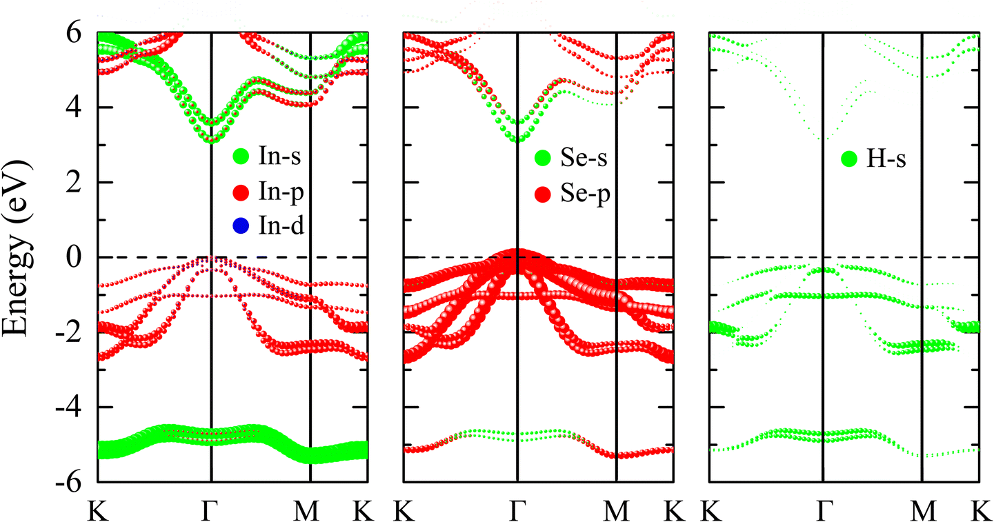 | ||
| Fig. 4 Orbital-projected band structure of 2H–InSe monolayer. The intensities of the bands correspond to the size of spheres. | ||
The adsorption of hydrogen can also significantly influence the work function of the InSe monolayer. As in other 2D materials, the adatoms can modify the electronic properties, including the work function, by altering the charge carrier concentration and the electronic band structure.52,53 As illustrated in Fig. 5(a), the work function Φ is defined as the energy difference between the Fermi level and the highest electrostatic potential above the surfaces of the 2H–InSe monolayer. It represents the work done to completely remove an electron from the monolayer’s surface. Previous studies have predicted that the work function of undoped InSe monolayers is approximately 4.5 eV,54 which can increase or decrease depending on the nature of dopant and its concentration.55 In this study, the full hydrogenation of the InSe monolayer increases the work function to 6.08 eV. As shown in Fig. 5(b), the charge transfer, results in a negative charge layer (blue regions) on the surface which increase the difficulty of removing electrons from the surface and making the work function increase.
 | ||
| Fig. 5 (a) Electrostatic potential of the 2H–InSe monolayer plotted along the z-direction, referenced to the Fermi level, and (b) electron density difference, where yellow regions represent electron depletion and blue regions indicate electron accumulation. | ||
To provide better understanding of the orientation of the orbitals in the 2H–InSe monolayer, the distribution of electron density was calculated and is presented in Fig. 5(b), where the Bader charge transfers are also indicated. The electronegativity of In is 1.78, while that of H is 2.2, therefore the hydrogen atom strongly attracts electrons to its site with a Bader charger of 0.529e. Meanwhile, the In atom loses its electrons with a Bader charge of −0.916e, and the Se atom gets electrons with a Bader charge of 0.387e. This results in two individual bond dipoles pointing from In atoms to H and Se atoms. The magnitudes of these dipoles can be visualized based on the distribution of electron density shown in Fig. 5(b), where regions with electron gain are in blue and regions with electron loss are in yellow. It is obvious that the charge polarity in the In–H bond is stronger than that in In–Se. Therefore, the In–H bond has a larger dipole moment than the In–Se bond. Moreover, the two dipoles, as shown in Fig. 5(a), point to different directions, causing a non-zero net dipole moment. Therefore, the unit cell of the 2H–InSe monolayer acts as a polar molecule.56 While having a non-zero net dipole moment, the crystal structure of 2H–InSe also lacks inversion symmetry in its non-stressed state, as shown in Fig. 1(a). These characteristics guarantee a good piezoelectric property57 where the stress-induced reorientation of individual dipoles can lead to a non-zero net polarization of charge in the 2H–InSe monolayer.
3.3 Elastic and piezoelectric properties of 2H–InSe monolayers
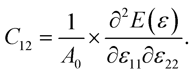
Monochalcogenides MX (where M = Sn, Ge and X = S, Se) are known to exhibit significant e11 and d11 piezoelectric coefficients58 due to their non-centrosymmetric structure. The 2H–InSe monolayer, which shares structural similarities with these materials and lacks inversion symmetry, is also expected to exhibit notable piezoelectric behavior. To accurately evaluate its piezoelectric coefficients e11 and d11, a comprehensive understanding of the monolayer’s elastic properties is essential. For 2D materials, the elastic constants Cij can be derived from the second derivatives of the total energy E(ε) with respect to the applied strain ε, and normalized by the equilibrium unit cell area A0,
 | (1) |
To obtain a differentiable function, the total energy E(ε) of slightly strained structures was fitted to a parabolic function. For the 2H–InSe monolayer, this fitting was performed for uniaxial strains ε11 and ε22 ranging from −1.5% to 1.5%. The elastic constants C11 and C12 were then determined as follows:
 | (2) |
 | (3) |
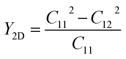
The Young’s modulus and Poisson’s ratio of the 2H–InSe monolayer are determined as follows:
 | (4) |
 | (5) |
The calculated elastic constants for the 2H–InSe monolayer are C11 = 59.15 N m−1, C12 = 18.40 N m−1 and C66 = (C11 − C12)/2 = 20.34 N m−1. These values satisfy Born’s stability criteria for a 2D hexagonal structure,59–61 where C11 > 0 indicates resistance to uniaxial stretching or compression, and C11 > C12 ensures resistance to shear deformation.
With a Young’s modulus of 53.43 N m−1, the 2H–InSe monolayer is significantly more flexible than graphene, which has a much higher Young’s modulus of approximately 340 N m−1.65 Despite this, its stiffness is comparable to that of other group III–VI monolayers such as pristine InSe, GaS, GaSe, InS, and InTe.62,66 The calculated Poisson’s ratio ν for 2H–InSe is 0.31, placing it within the typical range for stable solids (0.25 < ν < 0.35) and within the bounds observed for other two-dimensional materials (0.30 < ν < 0.70).67–69 This relatively lower Poisson’s ratio suggests that 2H–InSe will undergo less lateral contraction under uniaxial tension compared to pristine InSe, GaS, and GaSe monolayers, which exhibit higher ν values.62
The piezoelectric coefficients can be computed using the modern theory of polarization.70–74 This approach, based on Berry phase formalism, can create the polarization Pi as a function of second-rank strain εjk and stress σjk tensors. Having the polarization function Pi, the third-rank piezoelectric tensors eijk and dijk can be calculated as follows:63
 | (6) |
 | (7) |
As 2D materials are confined to the xy-plane, only in-plane strains, εxx, εyy, and εxy, are relevant, so jk = 11, 22, and 12 (=21). For 2D materials belonging to the D3h point group, such as the InSe monolayer, the non-zero piezoelectric coefficients are e11 and d11.63,75 Upon hydrogenation (2H–InSe), the symmetry of the InSe monolayer becomes slightly distorted, potentially altering its piezoelectric response – making this an interesting subject for further investigation. The piezoelectric coefficient e11 was calculated using eqn (6) and (7), while d11 = e11/(C11 − C12). The piezoelectric coefficients of 2H–InSe and other monolayers are reported in Table 2.
As indicated in Table 2, the calculated piezoelectric coefficients for the 2H–InSe monolayer (e11 = 1.53 × 10⁻¹⁰ cm−1 and d11 = 3.75 pm V−1) are comparable to those of the GaSe and GaS monolayers.62 Notably, these values represent an enhancement over the pristine InSe monolayer and position 2H–InSe as a promising candidate among popular piezoelectric materials such as MoS2 and hBN monolayers. These well-studied materials (MoS2 and hBN) are known for their effectiveness in practical devices, demonstrated through applications such as power generation (2 m Wm−2 at 0.53% strain), energy harvesting from motion or the micro-electro-mechanical systems (MEMS), self-powered ammonia sensors, oscillators, and ferroelectric memories.76–81 Therefore, the comparable piezoelectric response of 2H–InSe signifies its potential for many applications including electronics and MEMS.
3.4 Carrier concentration and temperature dependence of transport properties in 2H–InSe monolayers
InSe monolayers have demonstrated potential for promising electronic and optoelectronic applications, such as field-effect transistors and photoelectric converters.1,37 However, their performance is often restricted by intrinsic properties, notably a direct band gap and low hole mobility. To overcome these limitations, strategies such as applying strain, integrating InSe with other 2D materials, or molecular adsorption, have been explored.12,13,82 While these methods have yielded performance improvements, further analysis is necessary to provide better understanding about the effects of these modifications on the electronic structures of InSe monolayers. For instance, modifications like elemental substitution can dramatically change the carrier concentration, which directly affects the charge carrier mobility. Besides, the total mobility of InSe monolayers have also been shown to be strongly affected by carrier scattering mechanisms.13,83As established in previous sections, full hydrogenation significantly modifies the electronic structure and spatial charge density distribution of InSe, forming 2H–InSe. This makes 2H–InSe an ideal model system to systematically investigate the distinct and combined effects of carrier concentration, temperature, and scattering mechanisms on charge carrier mobility. The charge carrier mobility of the 2H–InSe monolayer is explored within the temperature range 50 K to 400 K. To determine the suitable carrier concentration interval for the 2H–InSe monolayer, it is worth noting that in 2D materials, charge carrier mobility typically increases with carrier concentration until a critical threshold. This rise is due to the enhanced screening of charged impurities, which effectively reduces scattering and improves carrier transport.84,85 However, a carrier concentration threshold higher than 1011 to 1013 cm−2 (corresponding to approximately 1015 to 1019 cm−3) leads to a rapid decline in mobility. This decrease is caused by the growth of scattering mechanisms such as ionized impurity (IMP) and polar optical phonon (POP) scattering, which become dominant factors in carrier transport. For instance, MA2N4 monolayers (where M = Mo, W; A = Si, Ge) exhibit constant mobility at low carrier concentrations, but experience a sharp decrease above 1 × 1013 cm−2.86 Similarly, graphene mobility drops from 10![[thin space (1/6-em)]](https://www.rsc.org/images/entities/char_2009.gif) 000–15000 cm2 V−1 s−1 to 4000–10000 cm2 V−1 s−1, 87,88 and MoS2 monolayer mobility decreases from 30–50 cm2 V−1 s−1 to 10–20 cm2 V−1 s−1.89 Therefore, this study investigates the transport properties of 2H–InSe monolayers at carrier concentrations of 1 × 10¹⁶ and 1 × 1020 cm−3, representing low and high regimes, respectively.
000–15000 cm2 V−1 s−1 to 4000–10000 cm2 V−1 s−1, 87,88 and MoS2 monolayer mobility decreases from 30–50 cm2 V−1 s−1 to 10–20 cm2 V−1 s−1.89 Therefore, this study investigates the transport properties of 2H–InSe monolayers at carrier concentrations of 1 × 10¹⁶ and 1 × 1020 cm−3, representing low and high regimes, respectively.
According to Matthiessen’s rule,30,90 the total mobility μtotal, is determined by the contributions of various scattering mechanisms, including acoustic deformation potential μADP, ionized impurity μIMP, piezoelectric μPIE, and polar optical phonon μPOP scattering. This relationship is expressed as .30,91 By applying this rule, the total electron μe and hole μh mobilities are calculated and presented in Fig. 6, along with the individual contributions from each scattering mechanism.
 | ||
| Fig. 6 Electron and hole mobilities (μe, μh) vs. temperature for a 2H–InSe monolayer at (a) 1016 cm−3 and (b) 1020 cm−3 carrier concentrations. | ||
In polar 2D materials like the 2H–InSe monolayer, strong Fröhlich coupling enhances polar optical phonon scattering (POP) at low carrier concentrations.92 As illustrated in Fig. 6(a), at a concentration of 1016 cm−3, the total electron mobility μe is 419.31 cm2 V−1 s−1 at 150 K. At 150 K, the dominance of POP scattering is characterized by a low mobility μPOP of 821 cm2 V−1 s−1. Meanwhile, the ionized impurity, piezoelectric, and acoustic phonon interactions are relatively weak at this doping level leading to higher scattering mobilities. The total hole mobility, 71.94 cm2 V−1 s−1, is significantly lower than the electron mobility. The hole mobility is also primarily limited by POP scattering with μPOP of 96.1 cm2 V−1 s−1, a consequence of the material’s polar nature amplifying phonon interactions. Conversely, at a high carrier concentration of 1020 cm−3 (Fig. 6(b)), the ionized impurity scattering becomes dominant, resulting in μIMP values of 7.27 cm2 V−1 s−1 and 12.3 cm2 V−1 s−1 at 150 K for electrons and holes, respectively. This intense impurity scattering strongly reduces the total electron and hole mobilities to 6.93 cm2 V−1 s−1 and 8.94 cm2 V−1 s−1, respectively, indicating the typical effect of dense impurity scattering in monolayers.90
As the temperature increases from 50 K to 400 K, the phonon scattering becomes more significant leading to changes in the contribution of each scattering to the total electron/hole mobility.92,93 At a low carrier concentration of 1016 cm−3, the population of polar phonons quickly increases, leading to a sharp decline of μPOP from around 105 to 101 cm2 V−1 s−1. Such strong decrease mainly causes the sharp decline in total mobility of electron and hole. The total electron mobility μe drops from 546.55 to 45.55 cm2 V−1 s−1, while the total hole mobility falls from 93.21 to 6.51 cm2 V−1 s−1. At a high carrier concentration of 1020 cm−3, as shown in Fig. 6(b), the ionized impurity scattering becomes the most dominant in the whole temperature range. The low μIMP together with the fast decrease of μPOP result in low total mobility of both electron and hole. However, the high values of μADP and μPIE mobilities help to maintain the decreasing tendency of total mobilities. The total electron mobility is 7.16 cm2 V−1 s−1 at 50 K and it decreases to 5.90 cm2 V−1 s−1 at 400 K. Meanwhile, the hole mobility falls from 11.58 cm2 V−1 s−1 to 3.55 cm2 V−1 s−1.
4 Conclusions
This study investigated the properties of the fully hydrogenated 2H–InSe monolayer using first-principles calculations. The dynamic stability of this monolayer was confirmed by the absence of imaginary modes in its phonon dispersion. Furthermore, its mechanical stability, flexibility, and resistance to lateral contraction were approved by its elastic constants, Young’s modulus, and Poisson’s ratio. Compared to pristine InSe monolayers, the fully hydrogenated 2H–InSe monolayer exhibited slightly reduced bond lengths and lattice constants. Analysis of the electronic structure, specifically the band structure and density of states (DOS), revealed that this reduction arises from the hybridization of H-s and In/Se-p orbitals. This hybridization forms strong covalent bonds, leading to the observed structural changes. Moreover, this orbital hybridization also resulted in a larger bandgap and a transition from an indirect to a direct bandgap. Notably, the directional nature of the s–p orbital hybridization, coupled with the lack of inversion symmetry, makes the 2H–InSe monolayer a promising candidate for piezoelectricity. Additionally, full hydrogenation induced charge redistribution, resulting in a non-zero net dipole moment. The calculated piezoelectric coefficients for the hydrogenated 2H–InSe monolayer were higher than those of pristine InSe, highlighting its potential as a piezoelectric material. Finally, the effect of carrier concentration and temperature on the total charge carrier mobility of the 2H–InSe monolayer were also examined. At a low carrier concentration of 1016 cm−3, optical phonon scattering (POP) was found to be the dominant scattering mechanism. However, at a high carrier concentration of 1020 cm−3, ionized impurity scattering (IMP) became dominant. The study revealed that electron mobility is higher than hole mobility, and both increase with rising temperature. In conclusion, this study demonstrates the promising application of fully hydrogenated 2H–InSe monolayers in piezoelectric devices. It also provides a comprehensive understanding of how hydrogen adsorption significantly alters the structural, electronic, piezoelectric, and transport properties of the 2H–InSe monolayer.Data availability
The data that support the findings of this study are available upon reasonable request from the corresponding author.Conflicts of interest
There are no conflicts of interest to declare.References
- D. Zheng, P. Chen, Y. Liu, X. Li, K. Liu, Z. Yin, R. Frisenda, Q. Zhao and T. Wang, J. Mater. Chem. A, 2024, 12, 16952–16986 RSC.
- A. Politano, D. Campi, M. Cattelan, I. Ben Amara, S. Jaziri, A. Mazzotti, A. Barinov, B. Gürbulak, S. Duman and S. Agnoli, et al., Sci. Rep., 2017, 7, 3445 CrossRef CAS PubMed.
- M. J. Hamer, J. Zultak, A. V. Tyurnina, V. Zólyomi, D. Terry, A. Barinov, A. Garner, J. Donoghue, A. P. Rooney and V. Kandyba, et al., ACS Nano, 2019, 13, 2136–2142 CAS.
- M. Wu, J.-j. Shi, M. Zhang, Y.-m. Ding, H. Wang, Y.-l. Cen and J. Lu, Nanoscale, 2018, 10, 11441–11451 RSC.
- B. Abay, H. Efeoğlu and Y. Yoğurtçu, Mater. Res. Bull., 1998, 33, 1401–1410 CrossRef CAS.
- Q. Zhao, R. Frisenda, T. Wang and A. Castellanos-Gomez, Nanoscale, 2019, 11, 9845–9850 RSC.
- I. B. Amara, A. Hichri and S. Jaziri, J. Phys.: Condens. Matter, 2017, 29, 505302 CrossRef PubMed.
- H.-C. Chang, C.-L. Tu, K.-I. Lin, J. Pu, T. Takenobu, C.-N. Hsiao and C.-H. Chen, Small, 2018, 14, 1802351 CrossRef PubMed.
- N. T. Paylaga, C.-T. Chou, C.-C. Lin, T. Taniguchi, K. Watanabe, R. Sankar, Y.-h. Chan, S.-Y. Chen and W.-H. Wang, npj 2D Mater. Appl., 2024, 8, 12 CrossRef CAS.
- N. T. Han, J. Guerrero-Sanchez and D. Hoat, Nanoscale Adv., 2025, 7, 1443–1451 RSC.
- C. Zhang, X. Chen, B. Cao, H. Duan, Q. Sun and F. Ouyang, Appl. Surf. Sci., 2022, 579, 152190 CrossRef CAS.
- Q. Wang, L. Han, L. Wu, T. Zhang, S. Li and P. Lu, Nanoscale Res. Lett., 2019, 14, 1–9 CrossRef PubMed.
- Y.-m. Ding, J.-j. Shi, C. Xia, M. Zhang, J. Du, P. Huang, M. Wu, H. Wang, Y.-l. Cen and S.-h. Pan, Nanoscale, 2017, 9, 14682–14689 RSC.
- J. Pető, G. Dobrik, G. Kukucska, P. Vancsó, A. A. Koós, J. Koltai, P. Nemes-Incze, C. Hwang and L. Tapasztó, npj 2D Mater. Appl., 2019, 3, 39 CrossRef.
- D. Dissanayake, A. Ashraf, D. Dwyer, K. Kisslinger, L. Zhang, Y. Pang, H. Efstathiadis and M. Eisaman, Sci. Rep., 2016, 6, 21070 CrossRef CAS PubMed.
- H. Sun, Y. Shang, Y. Yang and M. Guo, J. Nanomater., 2018, 2018, 6863890 Search PubMed.
- K. Yang, Z. Cui, E. Li, D. Ma, Y. Shen, Z. Yuan and Y. Dong, Mater. Today Commun., 2022, 33, 104226 CrossRef CAS.
- I. Koz’mik, Z. Kovalyuk, I. Grigorchak and B. Bakhmatyuk, Izv. Akad. Nauk SSSR, Neorg. Mater.;(USSR), 1987, 23, 754–757 Search PubMed.
- I. Zhirko, Z. Kovalyuk, M. Pyrlja and V. Boledzyuk, Hydrogen Materials Science and Chemistry of Carbon Nanomaterials, 2005, pp. 519–530 Search PubMed.
- O. Balyts’ Kyi, Mater. Sci., 2011, 46, 473 CrossRef.
- J. Felton, E. Blundo, S. Ling, J. Glover, Z. R. Kudrynskyi, O. Makarovsky, Z. D. Kovalyuk, E. Besley, G. Walker and A. Polimeni, et al., Molecules, 2020, 25, 2526 CrossRef CAS PubMed.
- G. Kresse and J. Furthmüller, Phys. Rev. B: Condens. Matter, 1996, 54, 11169 CrossRef CAS PubMed.
- G. Kresse and D. Joubert, Phys. Rev. B: Condens. Matter, 1999, 59, 1758 CrossRef CAS.
- J. P. Perdew, K. Burke and M. Ernzerhof, Phys. Rev. Lett., 1996, 77, 3865 CrossRef CAS PubMed.
- J. Heyd, G. E. Scuseria and M. Ernzerhof, J. Chem. Phys., 2003, 118, 8207–8215 CrossRef CAS.
- S. Grimme, J. Antony, S. Ehrlich and H. Krieg, J. Chem. Phys., 2010, 132, 154104 CrossRef PubMed.
- A. Togo, L. Chaput, T. Tadano and I. Tanaka, J. Phys.: Condens. Matter, 2023, 35, 353001 CrossRef CAS.
- S. Nosé, J. Chem. Phys., 1984, 81, 511–519 CrossRef.
- A. M. Ganose, J. Park, A. Faghaninia, R. Woods-Robinson, K. A. Persson and A. Jain, Nat. Commun., 2021, 12, 2222 CrossRef CAS PubMed.
- L. Cheng and Y. Liu, J. Am. Chem. Soc., 2018, 140, 17895–17900 CrossRef CAS PubMed.
- S. Zhou, C.-C. Liu, J. Zhao and Y. Yao, npj Quantum Mater., 2018, 3, 16 CrossRef.
- R. Guo, R. Zhao, Y. Ge, Y. Liu and W. Wan, Appl. Phys. Lett., 2023, 123, 063102 CrossRef CAS.
- Q. Lu, L. Li, S. Luo, Y. Wang, B. Wang and F.-T. Liu, RSC Adv., 2023, 13, 18816–18824 RSC.
- M. Yagmurcukardes, Phys. Rev. B, 2019, 100, 024108 CrossRef CAS.
- T. Hu, J. Zhou and J. Dong, Phys. Chem. Chem. Phys., 2017, 19, 21722–21728 RSC.
- T. M. Duyen Huynh, T. D. Hien Nguyen and M.-F. Lin, ACS Omega, 2022, 7, 34868–34876 CrossRef CAS PubMed.
- J. Zhou, J. Shi, Q. Zeng, Y. Chen, L. Niu, F. Liu, T. Yu, K. Suenaga, X. Liu and J. Lin, et al., 2D Materials, 2018, 5, 025019 CrossRef.
- Y. I. Zhirko, Z. Kovalyuk, M. Pyrlja and V. Boledzyuk, Hydrogen Materials Science and Chemistry of Carbon Nanomaterials, 2007, pp. 325–340 Search PubMed.
- A. S. Nissimagoudar, J. Ma, Y. Chen and W. Li, J. Phys.: Condens. Matter, 2017, 29, 335702 CrossRef PubMed.
- X. Huang, Q. Cao, M. Wan and H.-Z. Song, Materials, 2022, 15, 6214 CrossRef CAS PubMed.
- H. Ullah, I. Shehzadi, A. U. Rahman, M. W. Iqbal and S. Khan, Cryst.Growth Des., 2023, 23, 511–523 CrossRef CAS.
- H. Li, B. Xu, D. Evans and J. E. Reutt-Robey, J. Phys. Chem. C, 2007, 111, 2102–2106 CrossRef CAS.
- Y. Qu, H. Pan and C. T. Kwok, Sci. Rep., 2016, 6, 34186 CrossRef CAS PubMed.
- J. Chen, X. Wu and A. Selloni, Phys. Rev. B: Condens. Matter Mater. Phys., 2011, 83, 245204 CrossRef.
- B. G. Janesko, T. M. Henderson and G. E. Scuseria, Phys. Chem. Chem. Phys., 2009, 11, 443–454 RSC.
- S. Gao, L. Liu, B. Wen and X. Zhang, Phys. Chem. Chem. Phys., 2021, 23, 6075–6083 RSC.
- H.-R. Chen, M. Wan, Z.-M. Li, W.-H. Zhong, S.-Y. Ye, Q.-Q. Jia, J.-Y. Li and L.-Z. Chen, Inorg. Chem., 2023, 62, 12018–12026 CrossRef CAS PubMed.
- Y. Zhirko, V. Trachevsky and Z. Kovalyuk, Hydrogen Storage, 2012, pp. 211–242 Search PubMed.
- X. Cheng, L. Guan and J. Tao, Results Phys., 2019, 14, 102416 CrossRef.
- L.-L. Yang, J.-J. Shi, M. Zhang, Z.-M. Wei, Y.-M. Ding, M. Wu, Y. He, Y.-L. Cen, W.-H. Guo and S.-H. Pan, et al., Chin. Phys. Lett., 2019, 36, 097301 CrossRef CAS.
- D. K. Sang, H. Wang, M. Qiu, R. Cao, Z. Guo, J. Zhao, Y. Li, Q. Xiao, D. Fan and H. Zhang, Nanomaterials, 2019, 9, 82 CrossRef PubMed.
- S. Mallawaarachchi, M. Premaratne, S. D. Gunapala and P. K. Maini, Phys. Rev. B, 2017, 95, 155443 CrossRef.
- K. Ku, J. F. Joung, H. Park, M.-G. Kim, S. Park and W. Kim, Adv. Funct. Mater., 2018, 28, 1801394 CrossRef.
- S. Gopalan, G. Gaddemane, M. L. Van de Put and M. V. Fischetti, Materials, 2019, 12, 4210 CrossRef CAS PubMed.
- W. Cheng and J. Ni, Semicond. Sci. Technol., 2022, 37, 095011 CrossRef CAS.
- C. Kittel and D. F. Holcomb, Am. J. Phys., 1967, 35, 547–548 CrossRef.
- A. Arnau and D. Soares, in Piezoelectric Transducers and Applications, Springer, 2009, pp. 1–38 Search PubMed.
- R. Fei, W. Li, J. Li and L. Yang, Appl. Phys. Lett., 2015, 107, 173104 CrossRef.
- F. Mouhat and F.-X. Coudert, Phys. Rev. B: Condens. Matter Mater. Phys., 2014, 90, 224104 CrossRef.
- M. Born and K. Huang, Dynamical Theory of Crystal Lattices, Oxford university press, 1996 Search PubMed.
- T. V. Vu, N. N. Hieu, N. T. Hiep, T. T. Trinh, A. Kartamyshev and H. V. Phuc, Phys. Chem. Chem. Phys., 2025, 27, 5131–5140 RSC.
- W. Li and J. Li, Nano Res., 2015, 8, 3796–3802 CrossRef CAS.
- K.-A. N. Duerloo, M. T. Ong and E. J. Reed, J. Phys. Chem. Lett., 2012, 3, 2871–2876 CrossRef CAS.
- H. Zhu, Y. Wang, J. Xiao, M. Liu, S. Xiong, Z. J. Wong, Z. Ye, Y. Ye, X. Yin and X. Zhang, Nat. Nanotechnol., 2015, 10, 151–155 CrossRef CAS PubMed.
- A. Teklu, C. Barry, M. Palumbo, C. Weiwadel, N. Kuthirummal and J. Flagg, Adv. Condens. Matter Phys., 2019, 2019, 8713965 Search PubMed.
- Z.-Y. Chen, M. Xiong, Z.-Y. Zeng, X.-R. Chen and Q.-F. Chen, Solid State Commun., 2021, 326, 114163 CrossRef CAS.
- G. N. Greaves, A. L. Greer, R. S. Lakes and T. Rouxel, Nat. Mater., 2011, 10, 823–837 CrossRef CAS PubMed.
- Y. Ding and Y. Wang, J. Phys. Chem. C, 2013, 117, 18266–18278 CrossRef CAS.
- L. Tao, C. Yang, L. Wu, L. Han, Y. Song, S. Wang and P. Lu, Mod. Phys. Lett. B, 2016, 30, 1650146 CrossRef CAS.
- P. Vogl, J. Phys. C: Solid State Phys., 1978, 11, 251 CrossRef CAS.
- R. Resta, Ferroelectrics, 1992, 136, 51–55 CrossRef CAS.
- R. King-Smith and D. Vanderbilt, Phys. Rev. B: Condens. Matter, 1993, 47, 1651 CrossRef CAS PubMed.
- T. V. Vu, K. M. Bui, K. V. Hoang, A. Kartamyshev, T. H. Ho, A. Lavrentyev, N. P. Anh, H. V. Phuc and N. N. Hieu, J. Phys. D: Appl. Phys., 2024, 57, 345304 CrossRef CAS.
- T. V. Vu, N. T. Hiep, V. T. Vi, H. V. Phuc, A. Kartamyshev and N. N. Hieu, J. Phys. D: Appl. Phys., 2025, 58, 105309 CrossRef CAS.
- A. Kartamyshev, N. N. Hieu, N. Poklonski, N. V. Hieu, T. V. Vu, A. Lavrentyev and H. V. Phuc, Mater. Sci. Semicond. Process., 2025, 187, 109102 CrossRef CAS.
- H. Pang, Z. Zheng, E. Li and L. Wang, J. Phys. Chem. C, 2025, 129, 2186–2193 CrossRef CAS.
- M. Noor-A-Alam and M. Nolan, ACS Appl. Mater. Interfaces, 2023, 15, 42737–42745 CrossRef CAS PubMed.
- A. Mahapatra, R. Ajimsha, D. Deepak, R. Aggarwal, S. Kumar, R. Venkatesh, S. S. Roy and P. Misra, et al., Nano Energy, 2023, 116, 108829 CrossRef CAS.
- W. Wu, L. Wang, Y. Li, F. Zhang, L. Lin, S. Niu, D. Chenet, X. Zhang, Y. Hao and T. F. Heinz, et al., Nature, 2014, 514, 470–474 CrossRef CAS PubMed.
- D. Zhang, Z. Yang, P. Li, M. Pang and Q. Xue, Nano Energy, 2019, 65, 103974 CrossRef CAS.
- P. Ares, T. Cea, M. Holwill, Y. B. Wang, R. Roldán, F. Guinea, D. V. Andreeva, L. Fumagalli, K. S. Novoselov and C. R. Woods, Adv. Mater., 2020, 32, 1905504 CrossRef CAS PubMed.
- X. Liu, J.-C. Ren, S. Zhang, M. Fuentes-Cabrera, S. Li and W. Liu, J. Phys. Chem. Lett., 2018, 9, 3897–3903 CrossRef CAS PubMed.
- W. Feng, W. Zheng, W. Cao and P. Hu, Adv. Mater., 2014, 26, 6587–6593 CrossRef CAS PubMed.
- E. Hwang and S. Das Sarma, Phys. Rev. B: Condens. Matter Mater. Phys., 2009, 79, 165404 CrossRef.
- S. Das Sarma, S. Adam, E. Hwang and E. Rossi, Rev. Mod. Phys., 2011, 83, 407–470 CrossRef CAS.
- W.-H. Xiao, K. Yang, R. D’Agosta, H.-R. Xu, G. Ouyang, G. Zhou, K.-Q. Chen and L.-M. Tang, Phys. Rev. B, 2024, 109, 115427 CrossRef CAS.
- K. I. Bolotin, K. J. Sikes, J. Hone, H. Stormer and P. Kim, Phys. Rev. Lett., 2008, 101, 096802 CrossRef CAS PubMed.
- J.-H. Chen, C. Jang, S. Xiao, M. Ishigami and M. S. Fuhrer, Nat. Nanotechnol., 2008, 3, 206–209 CrossRef CAS PubMed.
- J.-S. Kim, Y. Liu, W. Zhu, S. Kim, D. Wu, L. Tao, A. Dodabalapur, K. Lai and D. Akinwande, Sci. Rep., 2015, 5, 8989 CrossRef CAS PubMed.
- K. Seeger, Semiconductor Physics, Springer Science & Business Media, 2013 Search PubMed.
- T. V. Vu, N. T. Hiep, H. V. Phuc, B. D. Hoi, A. Kartamyshev and N. N. Hieu, Phys. Rev. B, 2024, 110, 235403 CrossRef CAS.
- K. Kaasbjerg, K. S. Thygesen and K. W. Jacobsen, Phys. Rev. B: Condens. Matter Mater. Phys., 2012, 85, 115317 CrossRef.
- T. Sohier, M. Calandra and F. Mauri, Phys. Rev. B, 2016, 94, 085415 CrossRef.
| This journal is © The Royal Society of Chemistry 2025 |