DOI:
10.1039/D5RA03492B
(Paper)
RSC Adv., 2025,
15, 25799-25810
Optimization of short-circuit current density for tailored active region in BiFeO3 layer: a computational step into 3rd generation perovskite solar cells
Received
18th May 2025
, Accepted 8th July 2025
First published on 21st July 2025
Abstract
The global energy crisis has intensified the search for sustainable and clean energy alternatives, with solar energy emerging as a promising solution. The global energy crisis has intensified the search for sustainable and clean energy alternatives, with solar energy emerging as a promising solution. This study investigates the performance of BiFeO3 (BFO)-based perovskite solar cells using COMSOL Multiphysics simulations, focusing on the optimization of layer thicknesses and material properties. The results demonstrate that varying the thickness of the electron transport layer, absorber layer (BFO), and hole transport layer significantly impacts the short-circuit current density (Jsc), open-circuit voltage (Voc), and power conversion efficiency. Key findings include an optimal BFO thickness of 1210 nm, which balances light absorption and recombination losses, and a peak efficiency of 11.80% was observed. The study highlights the potential of BFO as a multiferroic absorber layer for high-efficiency, low-cost solar cells, paving the way for advancements in renewable energy technology.
1 Introduction
Fossil fuels currently dominate as the primary energy source; however, their finite availability and extensive utilization have led to severe environmental consequences, including global warming and ecological degradation.1 Addressing these pressing challenges necessitates the development and optimization of alternative energy sources and among these, solar energy stands out as a clean, sustainable, and renewable option, offering immense potential for long-term energy solutions. Solar energy is harnessed through solar cells, which convert sunlight directly into electricity, and has emerged as a cornerstone of renewable energy technologies.2–7 Within the realms of solar technologies, third-generation solar cells, particularly perovskites solar cells (PSCs), have garnered significant attention due to their remarkable advancements in efficiency and performance. Employing perovskite materials as light absorbers, PSCs have demonstrated an extraordinary increase in efficiency, from 3.8% in 2009 to an impressive 22.1% by 2017.8 This progress is attributed to the exceptional properties of perovskites, including high charge carrier mobility, a tunable bandgap, and an outstanding absorption coefficient. Despite these achievements, PSCs face critical challenges, such as hysteresis effects, lead toxicity associated with lead-doped perovskites, stability issues under operational conditions, and the necessity for advanced encapsulation techniques to enhance their durability and commercial viability.9–12
Research on PSCs has led to the development of various structural configurations, including mesoporous, planar, and inverted planar architectures.13 The n-i-p planar structure, a fundamental design in PSCs, comprises a transparent electron transport layer (ETL), an absorber material (perovskite-based layer), and a hole transport layer (HTL). Among ETL materials, ZnO has emerged as a versatile component over the past five decades due to its excellent transparency in the visible and infrared spectra, a wide optical bandgap of 3.5 eV, and an exciton binding energy of 60 meV.14–16 ZnO has found applications in dye-sensitized solar cells and works as a piezoelectric element in surface acoustic wave devices.17 The development of new ferroelectric perovskite materials with high polarization and low bandgap is in progress and found materials such as BaTiO3, PZT, and Bi4Ti3O12.18–21 However, the wide band gaps (>3 eV) of these ferroelectric systems restrict their practical uses due to poor absorption of solar energy so reduction in the band gap to an appropriate range is therefore necessary for effective photovoltaic operation. A suitable metal cation can be substituted at the B-site of ABO3 structure to tune the band gap, which also affects the ferroelectric characteristics.22–24 Recently, BiFeO3 (BFO) has garnered considerable interest due to its multiferroic properties at ambient temperature. BFO exhibits a strong remanent polarization (∼100 μC cm−2), which facilitates efficient separation of photogenerated charge carriers. This property, combined with its superior ferroelectric and optical characteristics, suggests BFO as a more suitable candidate for high-performance solar cells compared to traditional ferroelectric systems.25 While PSCs employing spiro-OMeTAD as the HTL demonstrate significantly improved long-term operational stability, such advancements are largely confined to dry conditions or require advanced encapsulation technologies. These limitations highlight the ongoing need for material innovations and structural optimizations to ensure durability and efficiency under practical operating conditions. The lead-free composition, strong remanent polarization, and variable bandgap of BFO provide distinct benefits over other perovskite materials including MAPbI3, CsPbI3, and FAPbI3 that improve charge separation and lower recombination losses. These characteristics solve performance and environmental issues, making BFO a viable substitute for lead-based perovskites.26–28
While substantial progress has been made in simulating and optimizing conventional planar PSCs, ferroelectric based configurations those utilizing BFO as a photoactive layer have received comparatively little research attention, creating a significant knowledge gap regarding their photovoltaic potential.29,30 This study has aim to bridge this gap by conducting material detailed numerical simulation of 1D ZnO/BFO/Spiro-OMeTAD configuration featuring ZnO as the ETL, BFO as the ferroelectric absorber layer, and Spiro as HTL where the optimized layer thicknesses are symmetrically documented in Table 1. The simulation methodology employs a rigorous parametric approach, methodology varying the thickness of one layer (i.e. absorber layer) while keeping fixed thicknesses of other layers (i.e. ETL and HTL). Similarly, each layer's thickness was varied to find the optimized thicknesses of each layer, and then different back metal contacts were tested at room temperature. Furthermore, device's temperature was varied to analyze the performance of device at higher temperature at optimized thicknesses.31–34 The central objective of this investigation is to identify the solar cell performance specially short-circuit current density trend in varied absorber layer's thickness as well as impact of various metal contacts and temperature on device. The outcome of this research is anticipated to provide fundamental insights for the rational design of high-performance ferroelectric photovoltaics and establish BFO-based device architectures as promising candidates for the next generation optoelectronics applications, particularly in the domains of energy harvesting systems and polarization enhanced photo conversion devices where conventional perovskite materials face stability challenges.35–38
Table 1 Initial parameters of materials used for respective layers in 1D (ZnO/BFO/Spiro-OMeTAD) PSC
| Parameters |
ZnO (ETL)69,70 |
BiFeO3 (absorber layer)71 |
Spiro-OMeTAD (HTL)70,71 |
| Thickness (nm) |
75 |
800 |
10 |
| Band gap (eV) |
3.3 |
2.5 |
3 |
| Electron affinity (eV) |
3.8 |
3.3 |
1.9 |
| Relative permittivity |
6 |
6 |
3 |
| Effective density of states at CB (1/cm3) |
1 × 10²⁰ |
5 × 10¹⁸ |
1 × 10²⁰ |
| Effective density of states at VB (1/cm3) |
1 × 10²⁰ |
5 × 10¹⁸ |
1 × 10²⁰ |
| Electron thermal velocity (cm s−1) |
1 × 10⁷ |
1 × 10⁷ |
1 × 10⁷ |
| Hole thermal velocity (cm s−1) |
1 × 10⁷ |
1 × 10⁷ |
1 × 10⁷ |
| Electron mobility (cm2 V−1 s−1) |
150 |
80 |
2 |
| Hole mobility (cm2 V−1 s−1) |
25 |
25 |
1 × 10⁻² |
| Electron lifetime (ns) |
1 |
1 |
5 |
| Hole lifetime (ns) |
1 |
1 |
5 |
2 Theoretical work
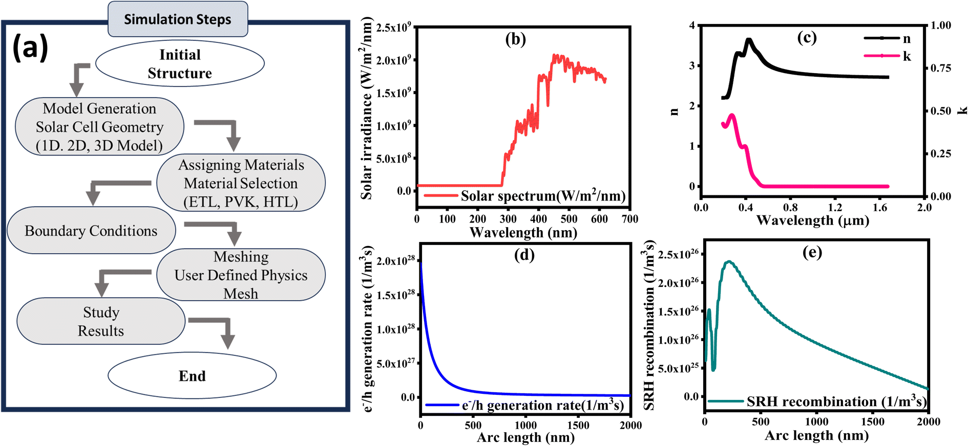
Poisson's equation and continuity equations are used to represent carrier transport when material parameters and layer thicknesses are defined at the start of the simulation procedure in COMSOL Multiphysics. To enhance the credibility of the simulation outcomes, mesh discretization and solver consistency analyses were performed, wherein COMSOL-based bifacial photovoltaic simulations demonstrated an error margin of 1.50% to 2.40% relative to experimental data. This affirms the high reproducibility achievable through appropriate meshing schemes and strict control of input parameters. Accordingly, all simulations in this study employed adaptive meshing strategies with convergence criteria calibrated to maintain output deviations below 2%, thereby reinforcing confidence in the numerical accuracy of the results.39 A clear and reproducible step-by-step guide to the simulation process is provided by the flowchart in Fig. 1(a). Poisson's equation and the carrier continuity equations were employed to model internal electric fields and charge carrier dynamics, based on established semiconductor physics frameworks as referenced in.40 The Poisson equation in one dimension is given as (eqn (1)):| |
 | (1) |
 |
| | Fig. 1 (a) Flow chart representing the major simulation steps, (b) solar irradiance, (c) solar absorption, (d) electron/hole generation rate and (e) SRH recombination. | |
Furthermore, to determine the electric potential or field, following equation is used (eqn (2)):
| |
 | (2) |
Here, in these equations (
eqn (1) and
(2)),
E represents electric field,
Ψ denotes the electrostatic potential,
q is the electron charge, and
ε is the dielectric constant of the semiconductor material. The hole and electron concentrations are represented by
p and
n, respectively, while
NA− and
ND+ refer to the densities of ionized acceptors and donors, respectively. Additionally,
ρt and
nt represent the concentrations of trapped holes and electrons, respectively, and
x is the position coordinate within the material.
41 A numerical model for PSCs, based on the continuity equations, accounts for the distinct operational mechanisms specific to perovskite materials. This model adapts the output voltage and current calculations to the unique properties of perovskites materials. The open-circuit voltage (
Voc) is influenced by carrier lifetimes and incident light intensity, while the short-circuit current density (
Jsc) is governed by the diffusion length and light intensity.
42 The continuity equation for electrons and holes is foundational for these calculations, and is given as (
eqn (3)):
| |
 | (3) |
Here,
n,
p(
x,
t) indicate the electron and hole concentrations, respectively, at position
x and time
t. The electron and hole current density,
J(n,p)(
x,
t) is also defined at the same spatial and temporal coordinates. Furthermore,
G(
x,
t) represents the generation rate of electron–hole pairs resulting from light absorption, while
R(
x,
t) represents the recombination rate, where electrons and holes recombine. The time derivative,
∂(
n,
p)(
x,
t)/
∂t, describes the temporal rate of change in the respective carrier densities.
43 Electrons and holes are the primary charge carriers in PSCs, contributing to the overall current generation through drift and diffusion mechanisms. For electron and hole transport, the total current density,
J(n,p), is the sum of drift and diffusion current densities, described as (
eqn (4)):
| |
 | (4) |
Here,
α =
n,
p while
D(n,p) is the electron/hole diffusion coefficient,
E is the electric field,
e is the elementary charge, and
μ(n,p) is electron/hole mobility. The hole mobility is derived using the Einstein relation,
μ =
eD/
kT, where
k is the Boltzmann constant, and
T is the temperature. This model utilizes the transport dynamics of both charge carriers within solar cell, facilitating insights into the contributions of both diffusion and drift to the overall current flow.
44,45
3 Device simulation and methodology
3.1 Solar spectrum and absorption
The solar irradiance spectrum plays a pivotal role in optimizing the performance of photovoltaic devices, particularly influencing the Jsc. Fig. 1(b) illustrates the solar irradiance under various conditions, with the AM1.5G standard (1000 Wm−2 nm−1) serving as the benchmark for terrestrial applications. This spectrum incorporates both direct and diffuse solar radiation. In contrast, the AM1.5D spectrum includes only direct sunlight, while the AM0 spectrum (1353 Wm−2 nm−1) is used for extraterrestrial calculations.46 The sun irradiance spectrum directly governs the photon flux reaching the photovoltaic material, which in turn determines the Jsc, as expressed below (eqn (5)):| |
 | (5) |
Here, Nph represents the photon flux, and the integral evaluates the current generated by photons with energies exceeding the material's bandgap. The theoretical maximum Jsc is ultimately constrained by factors such as reflection losses, series resistance, shunt losses, and recombination effects, which all limit the practical performance of the device. By converting spectral irradiance to photon flux and integrating over energies above the material's bandgap, the potential Jsc can be estimated, emphasizing the importance of selecting materials with optimal bandgap values. Fig. 1(c) shows the variation of the refractive index (n) and extinction coefficient (k) across different wavelengths, while Fig. 1(d) provides insight into the generation rate (G) of electron–hole pairs within the ZnO/BFO/Spiro solar cell at various depths and wavelengths. The generation rate is quantified using the following formula (eqn (6)):Here, α denotes the absorption coefficient, N0 the photon flux at the surface, and x is the depth within the material. Photons with shorter wavelengths (300–400 nm) are primarily absorbed near the cell's surface, resulting in high carrier generation rates in this region.47 From Fig. 1(d), this is reflected that the peak generation rate concentrated close to the surface, indicating efficient absorption of high-energy photons. As the depth increases, the generation rate diminishes, suggesting that lower-energy photons penetrate further into the material before being absorbed. Thus, optimizing the absorber layer thickness and material properties is crucial for enhancing carrier generation throughout the device.48 Fig. 1(e) highlights the depth-dependent Shockley–Read–Hall (SRH) recombination rate in this solar cell. The data indicates that recombination is most significant near the front surface, where carrier concentrations are highest due to the initial photon absorption. Beyond a depth of 200 nm, the recombination rate decreases, suggesting reduced carrier loss in the deeper regions of the cell. This emphasizes the necessity of surface passivation techniques to reduce recombination and improve overall cell efficiency. By minimizing surface recombination and optimizing the n & k values of BFO, it is possible to enhance charge collection and, consequently, the device's power conversion efficiency (PCE).49,50
3.2 Energy band diagram
Fig. 2(a) shows the schematic representation of 1D ZnO/BFO/Spiro solar cell along with front and back ohmic contacts. Fig. 2(b) represents the energy band structure of solar cell device, highlighting variations in energy levels as a functions of arc length (nm), which represents depth within a multilayered structure. As the arc length increases from 0 to 175 nm, the conduction band edge (Ec), valence band edge (Ev), and quasi-Fermi levels for electrons (Efn) and holes (Efp) display significant shifts, indicating non-homogeneous material properties. At an arc length of 1–75 nm (ZnO layer), the values of Ec, Efn, Efp, and Ev are 0.18 eV, 6.86 × 10⁻⁹ eV, −1.70 eV, and −2.32 eV, respectively. Then from 75–125 nm (BFO layer), these levels change to 1.11 eV, 0.56 eV, −0.90 eV, and −1.39 eV, reflecting alterations in the band structure likely due to material interfaces. These effects originate from band structure modifications at material interfaces, predominantly driven by electronic band bending, local electric fields arising from spontaneous polarization, and interface defect states that alter energy level alignment. The arc length 125–175 nm (Spiro layer), the energy levels reach at 2.88 eV for EC, 2.28 eV for Efn, −6.6 × 10⁻⁷ eV for Efp, and −0.11 eV for EV. The observed variations in Ec and Ev suggest region-dependent changes in the material bandgap, while shifts in Efn and Efp indicate non-equilibrium conditions influenced by factors like illumination or applied voltage (V), leading to distinct electron and hole concentration profiles. Fig. 2(c) shows the layers stacking with respect to the bandgap of layers for solar cell working. This analysis is crucial for understanding the electronic behavior of photovoltaic devices, such as solar cells.
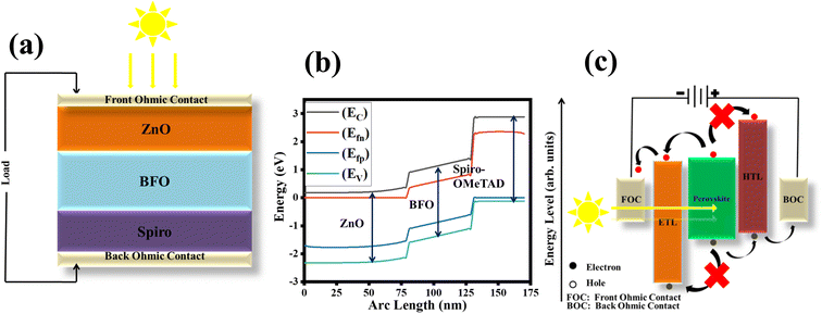 |
| | Fig. 2 (a) Solar cell configuration, (b) energy band diagram of ZnO/BFO/Spiro-OMeTAD based solar cell, and (c) solar cell layers formation. | |
Fig. 3 reveals the distinct bandgap values of the layers in the ZnO/BFO/Spiro solar cell, with ZnO, BFO, and Spiro exhibiting bandgap values of 3.3, 2.5, and 3 eV, respectively. The difference in band gaps is critical for efficient charge collection within the device. Due to ZnO's relatively wider bandgap, sunlight isn't absorbed within the ZnO layer, allowing photons to reach the underlying BFO active layer. When photons are absorbed by BFO, electron–hole pairs are generated. The well-designed band alignment ensures that the generated charge carriers are effectively separated and directed through the ETL and HTL to the metal contacts. The ohmic nature of the front and back contacts enables the effective extraction of accumulated charges, optimizing the device's overall efficiency.
 |
| | Fig. 3 Energy band diagram of a p–n junction in solar cells. | |
4 Results and discussion
4.1 Effect of BFO thickness on solar cell response
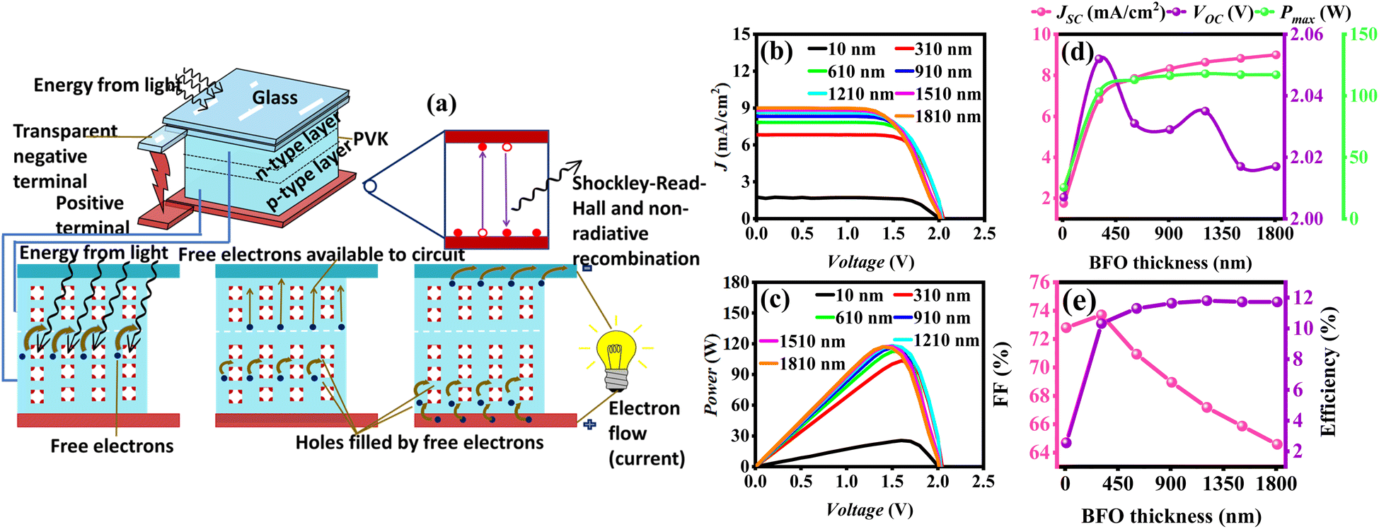
The absorbing layer is pivotal to study for the enhancement of performance of solar cell, as it avails the photo-induced charge carriers. When incident light shines on the front layer (i.e. glass surface) of solar cell, it may get reflected from there and then it penetrates through the ETL layer and reaches at absorbing layer. As the thickness of absorbing layer increases, it may increase the generation rate of photo-induced charge carriers, but this may happen up to the optimal thickness, after this thickness it may increase the recombination losses as well, as shown in Fig. 4(a).
 |
| | Fig. 4 (a) Schematic illustration of inside working mechanism of photo-induced charge carriers and recombination process, (b) J–V curve, (c) P–V curve of ZnO/BFO/Spiro-OMeTAD solar cell and effect of BFO's thickness variation on (d) Jsc,Voc,Pmax and (e) % FF and % efficiency. | |
The analysis of varying BFO thickness, ranging from 10 nm to 1810 nm, highlights its impact on photovoltaic parameters. As shown in Fig. 4(b), an increase in BFO thickness leads to a corresponding rise in J, with values escalating from 1.59 mA cm−2 at 10 nm to 8.37 mA cm−2 at 1810 nm. This increase is linked to improved photon absorption and subsequent generation of charge carriers. The maximum power output (P) as shown in Fig. 4(c), rises in same pattern as for J, with the maximum P increasing from 25.58 W at 10 nm to 117.18 W at 1810 nm. This trend suggests that thicker BFO layers enhance power generation by increasing the active region for light absorption. However, beyond a certain thickness, further increases in layer thickness result in diminishing returns, attributed to the onset of internal resistance and recombination losses.51 Furthermore, Fig. 4(d) shows the variation of Jsc,Voc, and maximum power (Pmax) at different BFO thicknesses, where Jsc is increasing as the BFO thickness increases, proving that expansion in active region causes to increase Jsc, while the corresponding changes in Pmax. The Voc, however, with a slight increase from 2 V to 2.01 V, indicating that the thickness has a minimal influence on Voc due to effective charge separation across the range. Fig. 4(e) shows the variation of % fill factor (FF) and efficiency for different values of BFO thicknesses, as FF decreases from 72.79% at 10 nm to 64.57% at 1810 nm, reflecting that excessive thickness hinders charge extraction efficiency despite the initial benefits in light absorption. On the other hand, there is a gradual increase in efficiency with thickness up to around 1000 nm, after which a slight decline is observed. At 10 nm, efficiency is approximately 2.55%, and it increases to 11.71% at 1810 nm. Thus, an optimal BFO thickness near 1000 nm is suggested for balancing light absorption and charge collection, ensuring better performance while mitigating recombination losses.52,53 The reduction in efficiency at wavelengths above 700 nm is supported by the SRH recombination depth profile shown in Fig. 1(d). The increased recombination rate with depth indicates enhanced carrier losses within thicker BFO layer. All corresponding output characteristics are listed in Table 2.
Table 2 Designed device 1D (ZnO/BFO/Spiro-OMeTAD) performance parameters with varying absorber layer's (BFO) thickness
| BFO's thickness (nm) |
Jsc (mA cm−2) |
Voc (V) |
Pmax (W) |
FF% |
Efficiency% |
| 10 |
1.75 |
2.01 |
25.59 |
72.80 |
2.56 |
| 310 |
6.82 |
2.05 |
103.21 |
73.70 |
10.32 |
| 610 |
7.84 |
2.03 |
112.99 |
70.93 |
11.30 |
| 910 |
8.32 |
2.03 |
116.40 |
68.95 |
11.64 |
| 1210 |
8.64 |
2.04 |
118.07 |
67.18 |
11.81 |
| 1510 |
8.82 |
2.02 |
117.24 |
65.86 |
11.72 |
| 1810 |
8.99 |
2.02 |
117.18 |
64.58 |
11.72 |
4.2 Effect of ETL on solar cell response
The impact of varying ETL thickness on the performance of 1D ZnO/BFO/Spiro solar cell is significant, as shown in Fig. 5(a), the relationship between J–V graphs show a steep decline in J with increasing ETL thickness. The variation in ETL thickness from 10 nm to 90 nm exerts a substantial impact on the key performance metrics of the solar cell. Although, simulation results suggest that further reductions in ETL thickness can enhance device efficiency, this study limits the ETL thickness to the 10–90 nm, to maintain fabrication feasibility. ZnO layer thinner than 10 nm typically exhibit poor morphological uniformity and increased defect densities.54 Future research should investigate alternative deposition techniques or wide-bandgap materials capable of achieving sub-10 nm ETLs without compromising film integrity. It is also important to recognize that ETL thicknesses exceedingly approximately 100 nm are rarely implemented in practical devices, as they introduce significant optical attenuation and reduce charge carrier mobility. Nevertheless, in realistic photovoltaic architectures, ZnO ETLs are typically restricted to thicknesses below 100 nm. However, at a thickness of 10 nm, the J reaches at maximum value of 7.81 mA cm−2 at a voltage of approximately 1.5 V. However, this value diminishes to 6.01 mA cm−2 at 90 nm, attributed to enhanced recombination and resistive losses within the thickness layer.
 |
| | Fig. 5 (a) J–V curve, (b) P–V curve of ZnO/BFO/Spiro-OMeTAD solar cell and effect of ETL's thickness variation on (c) Jsc,Voc,Pmax and (d) % FF, % efficiency. | |
Fig. 5(b) further highlights that P decreases significantly with increasing thickness; the maximum power observed is 117.24 W at 10 nm with a 1.5 V, whereas it falls to 84.18 W at 90 nm with a slightly lower the voltage of 1.4 V. Fig. 5(c) shows the variation of Jsc,Voc, and Pmax at different thicknesses of ETL, and Jsc decreases as the ZnO thickness increases, indicating further evidence of higher recombination losses in thicker layers.55 Meanwhile, the Voc shows a minor decrease from 2.02 V at 10 nm to 2.01 V at 90 nm, this change is not sufficient to counterbalance the reduction in other parameters. Furthermore, Pmax drops drastically beyond 30 nm thickness. The % FF and % efficiency as shown in Fig. 5(d), % FF decreases from 65.75% to 65.60% as thickness increases, further reducing overall cell performance. Thus, optimal performance is observed at lower ZnO thicknesses, where carrier collection and Pmax are maximized.56,57 Similarly, efficiency decreases, as the curve reveals that it peaks at 11.72% for 10 nm layer thickness but drops sharply to 8.41% at 90 nm due to increased internal resistance and light trapping effects, which inhibit charge carrier mobility. The output characteristics for various ETL thicknesses in 1D ZnO/BFO/Spiro solar cell are tabulated in Table 3.
Table 3 Designed device 1D (ZnO/BFO/Spiro-OMeTAD) performance parameters with varying ETL (ZnO) thickness
| ETL thickness (nm) |
Jsc (mA cm−2) |
Voc (V) |
Pmax (W) |
FF% |
Efficiency% |
| 10 |
8.82 |
2.02 |
117.24 |
65.75 |
11.72 |
| 30 |
7.98 |
2.02 |
105.86 |
65.83 |
10.59 |
| 50 |
7.33 |
2.01 |
96.85 |
65.68 |
9.68 |
| 70 |
6.80 |
2.02 |
89.92 |
65.57 |
8.99 |
| 90 |
6.37 |
2.01 |
84.18 |
65.61 |
8.42 |
4.3 Effect of HTL on solar cell performance
The thickness variation of HTL from 10 nm to 90 nm significantly influences the performance parameters of the solar cell, as Fig. 6(a) shows the impact of thickness on J, exhibits a high value of 8.36 mA cm−2 at 10 nm and slightly increases to 8.40 mA cm−2 at 90 nm. This suggests that the thinner HTL layers facilitate better photocurrent generation by reducing recombination losses, although the observed increase in maximum J at higher thicknesses may indicate improved carrier collection.58,59 Fig. 6(b) demonstrates that maximum P remains nearly constant across the range of HTL thicknesses, with values of 117.15 W and 117.70 W at 10 nm and 90 nm, respectively. This stability suggests that while the HTL thickness does not have a substantial impact on power generation, slight variations in internal resistance could be contributing to the observed changes.60,61 Fig. 6(c) exhibits variation in Jsc,Voc, and Pmax at different thicknesses of HTL, and it shows a minor increase in Jsc with increasing HTL thickness, similarly, Voc decreases from 2.02 V at 10 nm to 2.01 V at 90 nm. This enhancement could be attributed to improved charge separation at the HTL interface, although this benefit may be limited at higher thicknesses due to increasing resistive losses. On the other hand, the Pmax remains relatively stable across varying HTL thicknesses. However, as shown in Fig. 6(d), the FF slightly increases from 64.46% to 65.03%, suggesting a trade-off in charge extraction efficiency with increasing layer thickness. Despite these variations, the efficiency remains nearly constant, with a minor drop from 11.71% to 11.77% as thickness increases, pointing to optimal HTL performance near the thinner range without significant gains at higher thicknesses.62–64 The corresponding output solar cell characteristics for different HTL layer thicknesses are listed in Table 4.
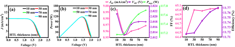 |
| | Fig. 6 (a) J–V curve, (b) P–V curve of ZnO/BFO/Spiro-OMeTAD solar cell and effect of HTL's thickness variation on (c) Jsc,Voc,Pmax and (d) % FF, % efficiency. | |
Table 4 Designed device 1D (ZnO/BFO/Spiro-OMeTAD) performance parameters with varying HTL layer's (Spiro-OMeTAD) thickness
| HTL thickness (nm) |
Jsc (mA cm−2) |
Voc (V) |
Pmax (W) |
FF% |
Efficiency% |
| 10 |
8.99 |
2.02 |
117.17 |
64.46 |
11.72 |
| 30 |
8.96 |
2.01 |
117.19 |
64.99 |
11.72 |
| 50 |
8.96 |
2.02 |
117.43 |
64.98 |
11.74 |
| 70 |
8.96 |
2.02 |
117.62 |
65.02 |
11.76 |
| 90 |
8.99 |
2.02 |
117.70 |
65.03 |
11.77 |
4.4 Effect of back metal contacts on solar cell response
In this study, 1D ZnO/BFO/Spiro solar cell is analyzed, employing a fixed chromium (Cr) front contact with a work function of 4.5 eV, while varying the back contact materials such as cobalt (Co), palladium (Pd), and nickel (Ni), with respective work functions of 4.92 eV, 5.12 eV, and 5.16 eV. The J–V and P–V characteristics for these contacts are shown in Fig. 7(a and b), and reveal that Co, due to its lower work function and improved charge extraction, achieves the highest J of 8.33 mA cm−2 at 1.2 V, leading to P ∼ 100.02 W. In contrast, Pd and Ni show same performance, with Jsc of 8.85 mA cm−2 and 8.85 mA cm−2, respectively, as shown in Fig. 7(c), and same trend is followed between Voc and metal contacts. The Pmax for Pd and Ni is 92.09 W and 90.62 W, respectively, occurring at slightly lower voltage values.65,66 Further, Fig. 7(d), demonstrates FF and efficiency, respectively, where Co achieves the highest efficiency ∼10% and FF ∼ 60.81%, while Pd and Ni, with higher work functions, exhibit efficiency ∼9.20% and 9.06%, respectively, due to greater carrier recombination and losses. The results underscore that selecting back contact with a lower work function, like Co, optimizes the cell's performance by enhancing charge collection and reducing recombination losses.67 The corresponding output characteristics of 1D ZnO/BFO/Spiro solar cell with using non-ohmic contacts at HTL side are tabulated in Table 5.
 |
| | Fig. 7 (a) J–V curve, (b) P–V curve of ZnO/BFO/Spiro-OMeTAD solar cell and effect of metal work function variation on (c) Jsc,Voc,Pmax and (d) % FF and % efficiency. | |
Table 5 Designed device 1D (ZnO/BFO/Spiro-OMeTAD) performance parameters with varying work function of back contacts
| Metal work function (eV) |
Jsc (mA cm−2) |
Voc (V) |
Pmax (W) |
FF% |
Efficiency% |
| Co (Φ) |
8.85 |
1.86 |
100.03 |
60.82 |
10.00 |
| Pd (Φ) |
8.85 |
1.76 |
92.10 |
59.09 |
9.21 |
| Ni (Φ) |
8.85 |
1.74 |
90.62 |
58.86 |
9.06 |
4.5 Effect of temperature on solar sell performance
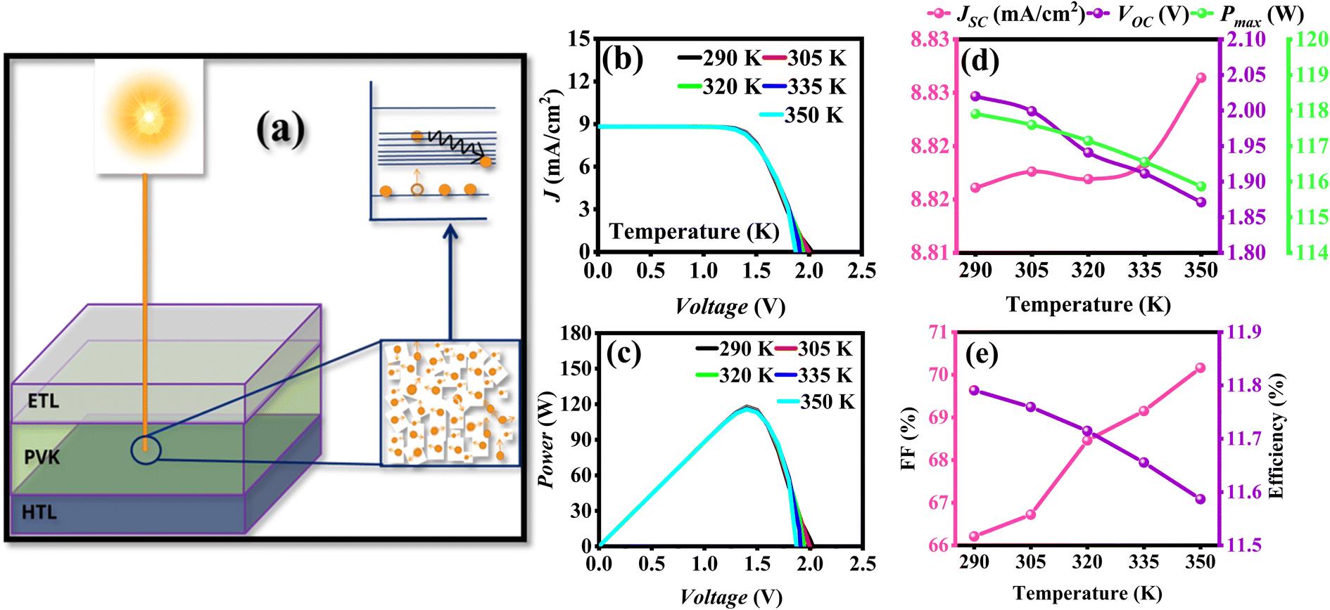
The impact of seasonal ambient temperature (ranging from winter to summer) on the performance of 1D ZnO/BFO/Spiro-based solar cells was analyzed. As the device temperature increases, the mobility of charge carriers also rises. However, excessive temperature can hinder carrier movement, increasing the solar cell's resistance, as shown in Fig. 8(a). Fig. 8(b) illustrates the J–V characteristics, where an increase in seasonal temperature from 290 K to 350 K leads to a progressive decrease in Voc from 2.02 V to 1.87 V, indicating reduced performance due to enhanced recombination and higher resistance. Additionally, the Voc experiences a slight decline due to elevated recombination rates at higher operating temperatures, this reduction is offset by corresponding increases in both Jsc and FF. As a result, the overall efficiency slightly decreases (from 11.79 to 11.58%), and on same temperature range P–V characteristics are shown in Fig. 8(c). Fig. 8(d) highlights variations in Jsc,Voc, and Pmax with temperature: Jsc slightly increases from 8.82 to 8.83 mA cm−2, Voc decreases from 2.02 to 1.87 V, and Pmax decreases from 117.90 to 115.86 W across the temperature range of 290–350 K. Fig. 8(e) shows the variation in FF and efficiency, with FF increasing as the temperature rises from 290 K to 350 K, aligning with theoretical optimal values. The overall efficiency decreases from 11.79 to 11.58% at elevated temperatures, emphasizing the importance of maintaining lower operational temperatures to optimize solar cell performance. The device's performance parameters at varying temperatures are summarized in Table 6.68
 |
| | Fig. 8 (a) Schematic illustration of the effect of increased temperature on charge carrier mobility and resistance in the solar cell, (b) J–V curve, (c) P–V curve of ZnO/BFO/Spiro-OMeTAD solar cell and effect of temperature variation on (d) Jsc,Voc,Pmax and (e) % FF and % efficiency. | |
Table 6 Effect of device surrounding's temperature on 1D (ZnO/BFO/Spiro-OMeTAD) PSC response
| Temperature (K) |
Jsc (mA cm−2) |
Voc (V) |
Pmax (W) |
FF% |
Efficiency% |
| 290 |
8.82 |
2.02 |
117.90 |
66.20 |
11.79 |
| 305 |
8.82 |
1.99 |
117.59 |
66.71 |
11.75 |
| 320 |
8.82 |
1.94 |
117.14 |
68.45 |
11.71 |
| 335 |
8.82 |
1.91 |
116.55 |
69.14 |
11.65 |
| 350 |
8.83 |
1.87 |
115.86 |
70.16 |
11.58 |
5 Conclusion
The study of varying thickness of ETL, BFO, and HTL in 1D ZnO/BFO/Spiro solar cells reveals key insights into their impact on performance. Increasing BFO active region thickness from 10 nm to 1810 nm enhances Jsc from 1.75 to 8.99 mA cm−2, though the Voc remains stable. Maximum power output rises, peaking at 118.06 W at 1210 nm, but efficiency increase from 2.55% to 11.80% due to charge carrier generation rates and minimal energy losses. For ZnO, efficiency peaks at 11.72% at 10 nm and declines sharply with increased thickness, reaching only 8.41% at 90 nm. The HTL thickness has minimal effect, with efficiency remaining nearly constant at 11.71% for 10 nm and 11.77% at 90 nm. Cobalt (Co), with a lower work function, provides the highest current density of 8.85 mA cm−2 and peak power output of 100.02 W, outperforming palladium (Pd) and nickel (Ni). Furthermore, the effect of variation in temperature gradient (from 290 K to 350 K) on solar cell performance showed that efficiency slightly decreases from 11.79% to 11.58% while it increases the Jsc from 8.82 to 8.83 mA cm−2. These findings suggest that optimal BFO and ZnO thicknesses, along with a low-work-function back contact like Co, enhance charge collection, reduce recombination, and maximize solar cell performance.
Data availability
The data will be available on request.
Conflicts of interest
There are no conflicts to declare.
Acknowledgements
The authors would like to acknowledge the Ongoing Research Funding Program (ORF-2025-71), King Saud University, Riyadh, Saudi Arabia.
References
- Z. Luo, P. Rong, Z. Yang, J. Zhang, X. Zou and Q. Yu, Preparation and application of co-doped zinc oxide: a review, Molecules, 2024, 29(14), 3373 CrossRef CAS PubMed.
- F. Cao, Y. Liu, M. Liu, Z. Han, X. Xu, Q. Fan and B. Sun, Wide bandgap semiconductors for ultraviolet photodetectors: Approaches, applications, and prospects, Research, 2024, 7, 0385 CrossRef CAS PubMed.
- M. Abdelfatah, A. M. El-Sayed, W. Ismail, S. Ulrich, V. Sittinger and A. El-Shaer, SCAPS simulation of novel inorganic ZrS2/CuO heterojunction solar cells, Sci. Rep., 2023, 13(1), 4553 CrossRef CAS PubMed.
- M. K. Hossain, G. I. Toki, A. Kuddus, M. H. Rubel, M. M. Hossain, H. Bencherif, M. F. Rahman, M. R. Islam and M. Mushtaq, An extensive study on multiple ETL and HTL layers to design and simulation of high-performance lead-free CsSnCl3-based perovskite solar cells, Sci. Rep., 2023, 13(1), 2521 CrossRef CAS PubMed.
- X. Zhou, J. Xu, S. Shi, J. Chen, J. Xu, L. Kong, X. Zhang and L. Li, Self-powered dual-wavelength polarization-sensitive photodetectors based on ZnO/BiFeO3 heterojunction, Appl. Surf. Sci., 2023, 623, 157032 CrossRef CAS.
- J. Lv and H. Ning, Photovoltaic effect of La and Mn Co-doped BiFeO3 heterostructure with charge transport layers, Materials, 2024, 17(9), 2072 CrossRef CAS PubMed.
- M. Huq, A. M. Jasi, P. Poure, S. Jovanovic, I. Revol and B. Lenoir, Critical analysis of optimized energy harvesting at small-scale by thermally coupled photovoltaic-thermoelectric systems, Renewable Sustainable Energy Rev., 2024, 195, 114331 CrossRef.
- F. V. Maziviero, D. M. Melo, R. L. Medeiros, Â. A. Oliveira, H. P. Macedo, R. M. Braga and E. Morgado Jr, Advancements and prospects in perovskite solar cells: From hybrid to all-inorganic materials, Nanomaterials, 2024, 14(4), 332 CrossRef CAS PubMed.
- S. Chander and S. K. Tripathi, Recent advancement in efficient metal oxide-based flexible perovskite solar cells: a short review, Mater Adv., 2022, 3(19), 7198–7211 RSC.
- C. Yadav and S. Kumar, Numerical simulation of novel designed perovskite/silicon heterojunction solar cell, Opt. Mater., 2022, 123, 111847 CrossRef CAS.
- A. Roy and M. Benhaliliba, Investigation of ZnO/p-Si heterojunction solar cell: Showcasing experimental and simulation study, Optik, 2023, 274, 170557 CrossRef CAS.
- A. Hedibi, A. Gueddim and B. Bentria, Numerical modeling and optimization of ZnO: Al/iZnO/ZnMgO/CZTS photovoltaic solar cell, Trans. Electr. Electron. Mater., 2021, 22, 666–672 CrossRef.
- L. P. Lekesi, L. F. Koao, S. V. Motloung, T. E. Motaung and T. Malevu, Developments on perovskite solar cells (PSCs): A critical review, Appl. Sci., 2022, 12(2), 672 CrossRef CAS.
- L. Zhu, Y. Xiang, Y. Liu, K. Geng, R. Yao and B. Li, Comparison of piezoelectric responses of flexible tactile sensors based on hydrothermally-grown ZnO nanorods on ZnO seed layers with different thicknesses, Sens. Actuators, A, 2022, 341, 113552 CrossRef CAS.
- A. Moradi, M. Maleki, S. R. Hosseini, M. Bahramgour, N. Delibas and A. Niaei, Thermal modeling of perovskite solar cells: Electron and hole transfer layers effects, Optik, 2024, 302, 171683 CrossRef CAS.
- J. Wang, J. Wang, J. Ding, Y. Wei and J. Zhang, Preparation of ZnO compact layer using vacuum ultraviolet for dye-sensitized solar cells, Solid State Sci., 2022, 127, 106860 CrossRef CAS.
- M. Benhaliliba, A rectifying Al/ZnO/pSi/Al heterojunction as a photodiode, Micro Nanostruct., 2022, 163, 107140 CrossRef.
- G. Chen, J. Chen, W. Pei, Y. Lu, Q. Zhang, Q. Zhang and Y. He, Bismuth ferrite materials for solar cells: Current status and prospects, Mater. Res. Bull., 2019, 110, 39–49 CrossRef CAS.
- K. Maity, J. F. Dayen, B. Doudin, R. Gumeniuk and B. Kundys, Graphene magnetoresistance control by photoferroelectric substrate, ACS Nano, 2024, 18(6), 4726–4732 CrossRef CAS PubMed.
- J. Ding, P. Zhao, H. Chen and H. Fu, Ultraviolet photodetectors based on wide bandgap semiconductor: a review, Appl. Phys. A, 2024, 130(5), 350 CrossRef CAS.
- S. Das, S. Ghara, P. Mahadevan, A. Sundaresan, J. Gopalakrishnan and D. D. Sarma, Designing a lower band gap bulk ferroelectric material with a sizable polarization at room temperature, ACS Energy Lett., 2018, 3(5), 1176–1182 CrossRef CAS.
- R. Yekani, H. Wang, P. Ghamari, S. Bessette, J. Sharir-Smith, R. Gauvin and G. P. Demopoulos, Impact of photo-induced doping of spiro-OMeTAD as HTL on perovskite solar cell hysteresis dynamics, J. Phys. Chem. C, 2024, 128(2), 710–722 CrossRef CAS.
- P. Lopez-Varo, L. Bertoluzzi, J. Bisquert, M. Alexe, M. Coll, J. Huang, J. A. Jimenez-Tejada, T. Kirchartz, R. Nechache, F. Rosei and Y. Yuan, Physical aspects of ferroelectric semiconductors for photovoltaic solar energy conversion, Phys. Rep., 2016, 653, 1–40 CrossRef CAS.
- S. Bhattarai, M. K. Hossain, J. Madan, R. Pandey, D. P. Samajdar, P. K. Kalita, A. N. Rashed, M. Z. Ansari and M. Amami, Performance improvement of CZTS-based hybrid solar cell with double hole transport layer using extensive simulation, J. Phys. Chem. Solids, 2023, 183, 111641 CrossRef CAS.
- H. Li, F. Li, Z. Shen, S. T. Han, J. Chen, C. Dong, C. Chen, Y. Zhou and M. Wang, Photoferroelectric perovskite solar cells: Principles, advances and insights, Nano Today, 2021, 37, 101062 CrossRef CAS.
- G. Tumen-Ulzii, T. Matsushima and C. Adachi, Mini-review on efficiency and stability of perovskite solar cells with Spiro-OMeTAD hole transport layer: Recent progress and perspectives, Energy Fuels, 2021, 35(23), 18915–18927 CrossRef CAS.
- Y. Shen, K. Deng and L. Li, Spiro-OMeTAD-based hole transport layer engineering toward stable perovskite solar cells, Small Methods, 2022, 6(11), 2200757 CrossRef CAS PubMed.
- F. M. Rombach, S. A. Haque and T. J. Macdonald, Lessons learned from spiro-OMeTAD and PTAA in perovskite solar cells, Energy Environ. Sci., 2021, 4(10), 5161–5190 RSC.
- Q. Zhou, D. Jiao, K. Fu, X. Wu, Y. Chen, J. Lu and S. E. Yang, Two-dimensional device modeling of CH3NH3PbI3 based planar heterojunction perovskite solar cells, Sol. Energy, 2016, 123, 51–56 CrossRef CAS.
- A. Hima, N. Lakhdar, B. Benhaoua, A. Saadoune, I. Kemerchou and F. Rogti, An optimized perovskite solar cell designs for high conversion efficiency, Superlattices Microstruct., 2019, 129, 240–246 CrossRef CAS.
- P. Sahoo, C. Tiwari, S. Kukreti and A. Dixit, All oxide lead-free bismuth ferrite perovskite absorber based FTO/ZnO/BiFeO3/Au solar cell with efficiency∼12%: First principle material and macroscopic device simulation studies, J. Alloys Compd., 2024, 981, 173599 CrossRef CAS.
- H. Chi, D. Liu, C. Ma, M. Song, P. Zhang and P. Dai, Simultaneously enhanced in-plane and out-of-plane thermal conductivity of a PI composite film by tetraneedle-like ZnO whiskers and BN nanosheets, ACS Appl. Polym. Mater., 2023, 5(9), 6909–6919 CrossRef CAS.
- E. Karamian and S. Sharifnia, Enhanced visible light photocatalytic activity of BiFeO3-ZnO pn heterojunction for CO2 reduction, Mater. Sci. Eng. B, 2018, 238, 142–148 CrossRef.
- M. Gartner, H. Stroescu, D. Mitrea and M. Nicolescu, Various applications of ZnO thin films obtained by chemical routes in the last decade, Molecules, 2023, 28(12), 4674 CrossRef CAS PubMed.
- C. Prakash and A. Dixit, Multifunctional BiFeO3 thin film-based memristor device as an efficient synapse:Potential for beyond von neumann computing in neuromorphic systems, ACS Appl. Electron. Mater., 2022, 4(12), 5763–5774 CrossRef CAS.
- A. S. Priya, D. Geetha, D. P. Pabba, R. Aepuru, Ș. Țălu and R. Varalakshmi, Prominent ferroelectric properties in multilayered TiO2 Mn-doped BiFeO3 spin-coated thin films, Ferroelectrics, 2024, 618(4), 957–969 CrossRef CAS.
- K. G. Beepat, D. P. Sharma, A. Mahajan, D. Pathak and V. Kumar, Simulation of multijunction solar cell interfaces for enhancement of the power conversion efficiency, Discover Appl. Sci., 2024, 6(6), 283 CrossRef CAS.
- M. I. Hossain, F. H. Alharbi and N. Tabet, Copper oxide as inorganic hole transport material for lead halide perovskite based solar cells, Sol. Energy, 2015, 120, 370–380 CrossRef CAS.
- J. M. Longares, A. García-Jiménez and N. García-Polanco, Multiphysics simulation of bifacial photovoltaic modules and software comparison, Sol. Energy, 2023, 257, 155–563 CrossRef.
- R. Stangl, C. Leendertz and J. Haschke, Numerical simulation of solar cells and solar cell characterization methods: The open-source on demand program AFORS-HET, Sol. Energy, 2010, 14, 319–352 Search PubMed.
- Y. Zhou and A. Gray-Weale, A numerical model for charge transport and energy conversion of perovskite solar cells, Phys. Chem. Chem. Phys., 2016, 18(6), 4476–4486 RSC.
- P. J. Manga, M. Maina, H. Samaila, E. W. Likta, R. O. Amusat and S. Daniel, Exploring the structural mechanics of titanium nickel solid alloy using COMSOL Multiphysics: A Poisson equation and continuity equation perspective, Sci. World J., 2024, 19(1), 71–77 CrossRef.
- A. Bablich, M. Müller, R. Bornemann, A. Nachtigal and P. Haring Bolívar, High responsivity and ultra-low detection limits in nonlinear a-Si: H pin photodiodes enabled by photogating, Photonic Sens., 2023, 13(4), 230415 CrossRef CAS.
- F. Brioua, C. Daoudi, B. Mekimah and B. Lekouaghet, The impact of a ZnO space layer on enhancing the efficiency of P3HT: PCBM blend-based organic solar cells, Phys. Scr., 2024, 99(8), 085951 CrossRef CAS.
- H. Asghar, T. Riaz, H. A. Mannan, S. M. Khan and O. M. Butt, Rheology and modeling insights into dye-sensitized solar cells (DSSCs) material: Bridging the gap to solar energy advancements, Renewable Sustainable Energy Rev., 2024, 193, 114298 CrossRef CAS.
- D. Lopez-Pascual, I. Valiente-Blanco, O. Manzano-Narro, M. Fernandez-Munoz and E. Diez-Jimenez, Experimental characterization of a geothermal cooling system for enhancement of the efficiency of solar photovoltaic panels, Energy Rep., 2022, 8, 756–763 CrossRef.
- L. Salgado-Conrado, C. Álvarez-Macías and B. Reyes-Durán, A review of simulation tools for thin-film solar cells, Materials, 2024, 17(21), 5213 CrossRef CAS PubMed.
- M. U. Shahid, N. M. Mohamed, A. S. Muhsan, S. N. Zaine, A. Yar, W. Ahmad, M. I. Irshad and M. B. Hussain, High-yield TiO2 submicron sphere/nanoparticle-blended scattering layer for efficient and scalable dye-sensitized solar cells, Emergent Mater., 2023, 6(2), 671–679 CrossRef CAS.
- A. S. Al-Ezzi and M. N. Ansari, Numerical analysis and performance study of a double-heterojunction GaAs-based solar cell, J. Comput. Electron., 2024, 23(2), 358–368 CrossRef CAS.
- M. U. Siddiqui, O. K. Siddiqui, A. B. Alquaity, H. Ali, A. F. Arif and S. M. Zubair, A comprehensive review on multi-physics modeling of photovoltaic modules, Energy Convers. Manage., 2022, 258, 115414 CrossRef.
- W. A. Wani, H. Renuka, S. Kundu, S. Goel, H. Venkataraman and K. Ramaswamy, What ails the photovoltaic performance in single-layered unpoled BFO?–The role of oxygen annealing in improving the photovoltaic efficiency, Sol. Energy, 2022, 236, 822–831 CrossRef.
- O. Ceballos-Sanchez, A. Sanchez-Martinez, F. J. Flores-Ruiz, A. M. Huerta-Flores, L. M. Torres-Martínez, R. Ruelas and M. García-Guaderrama, Study of BiFeO3 thin film obtained by a simple chemical method for the heterojunction-type solar cell design, J. Alloys Compd., 2020, 832, 154923 CrossRef CAS.
- M. Khan, M. A. Iqbal, M. Malik, S. U. Hashmi, S. Bakhsh, M. Sohail, M. T. Qamar, M. Al-Bahrani, R. Y. Capangpangan, A. C. Alguno and J. R. Choi, Improving the efficiency of dye-sensitized solar cells based on rare-earth metal modified bismuth ferrites, Sci. Rep., 2023, 13(1), 3123 CrossRef CAS PubMed.
- N. Rai, S. Rai, P. K. Singh, P. Lohia and D. K. Dwivedi, Analysis of various ETL materials for an efficient perovskite solar cell by numerical simulation, J. Mater. Sci.: Mater. Electron., 2020, 31, 16269–16280 CrossRef CAS.
- M. U. Salman, M. Mehak, U. Ali, G. M. Din, S. M. Ramay, M. Younis and S. Atiq, Direct correlation between open-circuit voltage and quasi-fermi level splitting in perovskite solar cells: a computational step involving thickness, doping, lifetime, and temperature variations for green solutions, RSC Adv., 2025, 15(20), 15618–15629 RSC.
- S. A. Graham, P. Manchi, M. V. Paranjape and J. S. Yu, Mechanical and acoustic-driven BiFeO3 composite films-based hybrid nanogenerator for energy harvesting and sensing applications, Small, 2024, 20(20), 2308428 CrossRef CAS PubMed.
- I. Qasim, O. Ahmad, A. Rashid, T. Zehra, M. I. Malik, M. Rashid, M. W. Ahmed and M. F. Nasir, Numerical optimization of (FTO/ZnO/CdS/CH3NH3SnI3/GaAs/Au) perovskite solar cell using solar capacitance simulator with efficiency above 23% predicted, Opt. Quantum Electron., 2021, 53, 1–8 CrossRef.
- A. Bag, R. Radhakrishnan, R. Nekovei and R. Jeyakumar, Effect of absorber layer, hole transport layer thicknesses, and its doping density on the performance of perovskite solar cells by device simulation, Sol. Energy, 2020, 196, 177–182 CrossRef CAS.
- P. Tiwari, M. F. Alotaibi, Y. Al-Hadeethi, V. Srivastava, B. Arkook, P. Lohia, D. K. Dwivedi, A. Umar, H. Algadi and S. Baskoutas, Design and simulation of efficient SnS-based solar cell using spiro-OMeTAD as hole transport layer, Nanomaterials, 2022, 12(14), 2506 CrossRef CAS PubMed.
- H. Abedini-Ahangarkola, S. Soleimani-Amiri and S. G. Rudi, Modeling and numerical simulation of high efficiency perovskite solar cell with three active layers, Sol. Energy, 2022, 236, 724–732 CrossRef CAS.
- G. A. Casas, M. Á. Cappelletti, A. P. Cedola, B. M. Soucase and P. y Blancá, Analysis of the power conversion efficiency of perovskite solar cells with different materials as hole-transport layer by numerical simulations, Superlattices Microstruct., 2017, 107, 136–143 CrossRef CAS.
- T. Du, W. Xu, S. Xu, S. R. Ratnasingham, C. T. Lin, J. Kim, J. Briscoe, M. A. McLachlan and J. R. Durrant, Light-intensity and thickness dependent efficiency of planar perovskite solar cells: Charge recombination versus extraction, J. Mater. Chem. C, 2020, 8(36), 12648–12655 RSC.
- B. Islam, A. Hosen, T. M. Khan, M. F. Rahman, M. H. Rahman, M. S. Islam and S. R. Ahmed, Simulating the effect of inserting Sb2S3 as hole transport layer on SnS-Based thin-film solar cells, J. Electron. Mater., 2024, 53(8), 4726–4739 CrossRef CAS.
- I. Hasan, T. M. Khan, B. Islam, M. F. Rahman and S. R. Al Ahmed, A comprehensive study to evaluate performances of Cs3Sb2I9-based perovskite solar cell with Spiro-OMeTAD HTL using SCAPS-1D simulator, Mater. Sci. Eng. B, 2024, 310, 117740 CrossRef CAS.
- T. A. Chowdhury, M. A. Zafar, M. S. Islam, M. Shahinuzzaman, M. A. Islam and M. U. Khandaker, Stability of perovskite solar cells: Issues and prospects, RSC Adv., 2023, 13(3), 1787–1810 RSC.
- R. Hosen, S. Sikder, M. S. Uddin, M. M. Haque, H. Mamur and M. R. Bhuiyan, Effect of various layers on improving the photovoltaic efficiency of Al/ZnO/CdS/CdTe/Cu2O/Ni solar cells, J. Alloys Compd., 2023, 4, 100041 Search PubMed.
- Z. Khan, M. Noman, S. T. Jan and A. D. Khan, Systematic investigation of the impact of kesterite and zinc based charge transport layers on the device performance and optoelectronic properties of ecofriendly tin (Sn) based perovskite solar cells, Sol. Energy, 2023, 257, 58–87 CrossRef CAS.
- M. Kumar, S. K. Pundir and D. V. Singh, Effect on green energy conversion and stability with ‘Er’modification in multiferroic based perovskite solar cell devices, Mater. Today Commun., 2024, 38, 107841 CrossRef CAS.
- A. Raj, M. Kumar, A. Kumar, K. Singh, S. Sharma, R. C. Singh, M. S. Pawar, M. Z. Yahya and A. Anshul, Comparative analysis of ‘La’modified BiFeO3-based perovskite solar cell devices for high conversion efficiency, Ceram. Int., 2023, 49(1), 1317–1327 CrossRef CAS.
- Y. K. Karmani, M. Bilal, M. U. Salman, M. Ameen, M. Luqman, S. M. Ramay, M. Younis and S. Atiq, Correlation between trap-assisted non-radiative recombination losses and thermal agitation in SnS-based solar cell: A state-of-the-art computational analysis, Mater. Sci. Eng. B, 2025, 321, 118484 CrossRef CAS.
- M. U. Salman, M. Bilal, Y. K. Karmani, U. Ali, S. M. Ramay, M. Younis and S. Atiq, Influence of acceptor/donor densities and layer thicknesses on the efficiency of 2D ZnO/BFO/spiro-OMeTAD perovskite solar cells: A COMSOL simulation-based optimization, J. Mater. Chem. A, 2025, 13(20), 15057–15066 RSC.
|
| This journal is © The Royal Society of Chemistry 2025 |
Click here to see how this site uses Cookies. View our privacy policy here. 
 Open Access Article
 This Open Access Article is licensed under a Creative Commons Attribution-Non Commercial 3.0 Unported Licence
 *a,
Muhammad Luqmana,
Shahid M. Ramayb,
Waqas Mahmoodc and
Shahid Atiq
*a,
Muhammad Luqmana,
Shahid M. Ramayb,
Waqas Mahmoodc and
Shahid Atiq