
 Open Access Article
 This Open Access Article is licensed under a Creative Commons Attribution-Non Commercial 3.0 Unported Licence
Synthesis and electrical properties of 2D cubic vanadium nitride†
Qiuyun Yang‡
 *ab,
Ziping Wang‡b,
Fanfan Shib,
Dehu Lib,
Yao Pengb and
Jianyi Liub
*ab,
Ziping Wang‡b,
Fanfan Shib,
Dehu Lib,
Yao Pengb and
Jianyi Liub
aInstitute of Electrical and Electronic Engineering, Anhui Science and Technology University, Fengyang 233100, China
bDepartment of Physics, University of Science and Technology of China, Hefei 230026, China. E-mail: yang1990@ustc.edu.cn
First published on 10th July 2025
Abstract
Due to the exceptional physical and chemical properties, vanadium nitride (VN) films exhibit significant potential for a wide range of applications. However, their non-layered structure has hindered their integration into two-dimensional nano-electronic devices, primarily due to the challenges associated with synthesizing well-defined 2D films. This study proposed an efficient method for the synthesis of 2D vanadium nitride films through a two-step growth process that combines chemical vapor deposition with atomic substitution. For the first time, VN films with thicknesses close to the atomic level were fabricated, and the relationship between the thickness and electrical properties was studied. Transmission electron microscopy (TEM) characterization demonstrated a well-defined crystalline structure and verified the cubic VN phase formation. X-ray photoelectron spectroscopy (XPS) coupled with chemical state analyses confirmed the exclusive composition of VN. Atomic force microscopy (AFM) quantification established ultrathin VN film thickness down to 3.2 nm, exhibiting exceptional surface uniformity. A four-electrode configuration was fabricated on VN films for sheet resistance evaluation, revealing thickness-dependent electrical characteristics, achieving an optimal sheet resistance of 16 Ω sq−1 at 68.1 nm. Transfer characteristic analysis conclusively confirmed metallic conduction behavior in the synthesized films. The temperature-dependent test showed the sheet resistance is insensitive to temperature change. This methodology establishes the efficacy of the atomic substitution method for fabricating non-layered 2D transition metal nitrides (TMNs) with enhanced functionality, offering crucial insights for developing next-generation nanoelectronics based on non-layered TMN architectures.
Introduction
Vanadium nitride (VN), a transition metal nitride (TMN),1 has attracted significant research attention due to the exceptional multifunctional properties of its thin films, particularly their synergistic combination of high mechanical hardness, thermal stability, and electrical conductivity. These attributes position VN as a versatile material for applications spanning functional coatings and energy-related technologies.2–8 As a non-layered compound, VN cannot be produced through conventional mechanical exfoliation methods typically employed for layered materials.9 Current synthesis strategies for VN films primarily include direct current reactive magnetron sputtering,10 chemical vapor deposition (CVD),11,12 atomic layer deposition (ALD),13 and vapor–liquid–solid (VLS) epitaxial growth.14 Despite these technological advancements, the fabrication of well-defined two-dimensional (2D) epitaxial VN films remains substantially more challenging compared to established 2D atomic crystals like graphene15 and WS2.16 This synthetic difficulty has resulted in limited fundamental understanding of 2D VN's intrinsic properties and application potential. Notably, material properties often exhibit dramatic transformations during dimensional reduction from three-dimensional (3D) bulk structures to 2D configurations,17 highlighting the critical need for developing reliable synthesis protocols for high-quality 2D VN films. Such methodological advancements are essential for unlocking the full potential of 2D VN in emerging nanotechnologies.Moreover, recent studies have confirmed that transition metal nitride (TMN) film thickness critically governs charge transport properties.18,19 The increased thickness reduce electron scattering yet amplify surface roughness. Surface smoothness proves essential for optimal conductivity, as morphological defects trap charge carriers.20 While vanadium nitride (VN) has been extensively studied as a representative TMN, the thickness-dependent electronic behavior in two-dimensional VN films remains unexplored. Consequently, establishing a precise correlation between vanadium nitride film thickness and electrical characteristics under controlled conditions of surface smoothness and dimensional stability becomes essential for performance optimization in micro/nano-electronic devices.
In this study, two-dimensional vanadium dioxide (VO2) films were synthesized through optimized chemical vapor deposition (CVD), followed by ammonia-assisted atomic substitution nitridation to obtain ultrathin VN films with controlled thickness down to 3.2 nm. Structural characterization using high-resolution transmission electron microscopy (HR-TEM) revealed a well-defined single-crystal cubic phase structure, consistent with fast Fourier transform (FFT) patterns. Surface morphology analysis via atomic force microscopy (AFM) demonstrated an ultra-smooth surface with a root-mean-square roughness below 0.4 nm. Systematic investigation of thickness-dependent electrical properties was conducted using four-probe measurements, revealing an inverse relationship for sheet resistance with increasing thickness. Notably, transfer characteristic curve tests confirmed the metallic nature of VN films. This work establishes the first experimental framework correlating thickness-engineering with electronic properties in 2D VN films, by providing: (i) direct evidence for the efficacy of atomic substitution methodology in non-layered material synthesis, and (ii) critical benchmarks for implementing VN in advanced nanoelectronics. The research offers a generalizable paradigm for synthesizing and characterizing emerging transition metal nitride systems.
Results and discussion
Fig. 1a schematically illustrates the fabrication workflow for two-dimensional VN thin films (procedural details provided in the Experimental section). As shown in Fig. S1 (see ESI),† optical microscopy images of as-grown VO2 crystals on mica substrates exhibit thickness-dependent colour variations (from 3.9 to tens of nanometers, correlated with interference contrast), and a representative single-crystalline domain with lateral dimensions exceeding 61 μm. Following transfer to SiO2/Si substrates (Fig. 1b), controlled ammonia nitridation was performed to achieve phase-pure VN crystals (Fig. 1c), with the observed chromatic shift (blue and purple to pink) serving as a visual indicator of completed nitridation. Comparative Raman spectroscopy analysis (Fig. 1d) revealed marked structural differences: (i) VO2 crystals displayed characteristic phonon modes at 141, 195, 224, 339, 385, 589, and 616 cm−1, which are consistent with the literature,21,22 while (ii) VN samples exhibited complete suppression of Raman activity, confirming successful conversion to metallic phase. To mitigate oxidation risks (e.g., VO2 to V2O5 or VN to VOx) induced by excessive laser power, Raman spectroscopy measurements were conducted using a laser with 1% power intensity (original intensity: 150 mW), and a 2400 grooves/mm grating.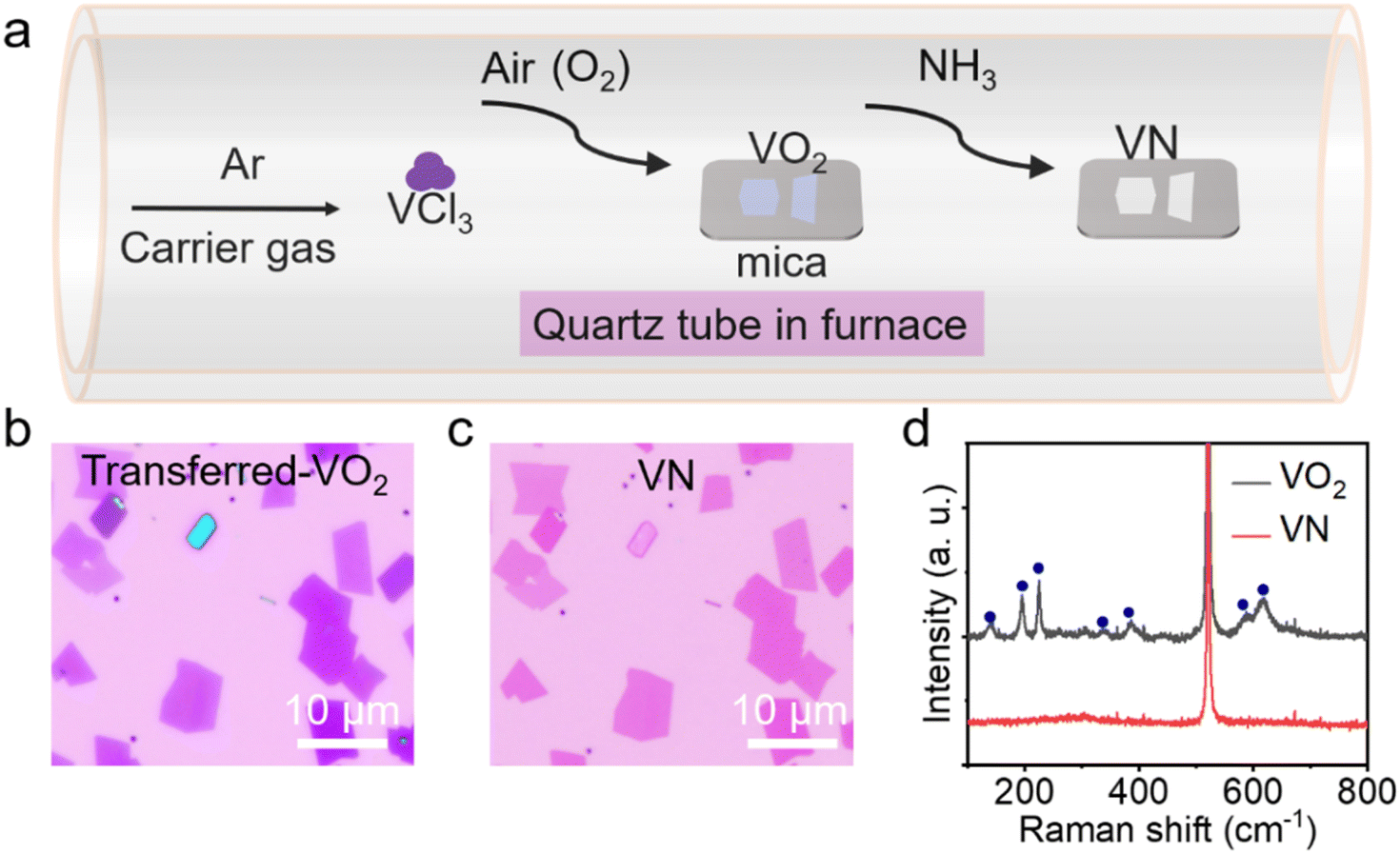 | ||
| Fig. 1 Schematic of the growth process of vanadium nitride and the characterization. (a) Schematic illustration of the growth process, encompassing the CVD synthesis of VO2 thin films and the atomic substitution method for preparation VN thin films. (b) Optical images of grown VO2 samples transferred onto SiO2/Si substrates. (c) Optical images of VN samples, obtained by nitriding the sample shown in (b). (d) Raman spectrum of the grown VO2 and VN, the Raman peaks of VO2 are marked with blue dots. | ||
Atomic force microscopy (AFM) was systematically performed to quantify the thickness evolution and surface topography of as-synthesized VO2 and its phase-transformed vanadium nitride (VN) derivative. As displayed in Fig. 2a, the AFM topography of a pristine VO2 crystal on SiO2/Si (lower-left inset: corresponding optical micrograph) reveals uniform film continuity. Fig. 2b demonstrates the morphological retention of the phase-transformed VN derived from the identical VO2 crystal in Fig. 2a. Cross-sectional height profiling (Fig. 2c) at matched spatial coordinates (blue: VO2; red: VN) documents a thickness reduction from 3.9 nm to 3.2 nm post-nitridation, attributable to atomic substitution-induced lattice contraction and structural reorganization during phase transformation.23 Critically, statistical analysis of surface roughness (identical scan areas) revealed a statistically significant reduction in root-mean-square roughness (Rq: 0.53 nm to 0.38 nm). This dual evidence—dimensional compaction and surface smoothing—not only confirm the ultra-flat morphology of VN films (<0.4 nm Rq) but also imply defect annihilation and interface optimization driven by the self-limiting nitridation mechanism.
 | ||
| Fig. 2 AFM characterization of a sample film before (VO2) and after nitride (VN). (a) and (b) Are AFM images at the same place on VO2 and VN sample (location marked by circle region in the left inset optical microscopy). (c) AFM height profile (along blue and red dashed lines in (a) and (b)) suggests the thickness reduced after nitriding. | ||
The microstructure of VO2 and VN crystals at the nanoscale was characterized by transmission electron microscopy (TEM) technology. As shown in Fig. 3a and d, the low-magnification TEM images of VO2 and VN films transferred onto the micro-grid copper meshes are presented. High-resolution TEM (HRTEM) provides phase-contrast images, permitting atomic-scale observation of the crystal structure in two-dimensional materials. Lattice plane indices (hkl) and interplanar spacings can be directly labeled on these micrographs. HRTEM imaging (Fig. 3b) of VO2 resolved periodic lattice fringes with spacings of 5.94 Å, 3.49 Å and 2.70 Å, indexed respectively to the (110), (102) and (212) crystallographic planes of metastable tetragonal VO2 (space group P42/nmc). Fast Fourier Transform (FFT) processing efficiently extracts diffraction information from HRTEM images, generating a frequency spectrum analogous to selected area electron diffraction (SAED) patterns. However, FFT-derived spectra offer higher resolution and provide direct spatial correlation with the imaged region. Corresponding FFT analysis (Fig. 3c) further confirmed the tetragonal symmetry via 26.0° and 45.8° interplanar angles between (102)–(212) and (212)–(110) diffraction spots, respectively (matching PDF #42-0876).24 For VN crystals (Fig. 3e), atomic-resolution imaging unveiled a characteristic cubic lattice with spacings of 2.05 Å and 1.46 Å, assigned to (200) and (220) planes of F m3m VN. FFT patterns (Fig. 3f) exhibited 44.4° and 45.3° interplanar angles among (200)–(220)–(200) diffraction spots, conclusively verifying cubic phase consistency (PDF #35-0768).25,26 In addition, selecting specific diffraction spots for Inverse Fast Fourier Transform (IFFT) reconstruction enables the visualization of local atomic arrangements. This technique is particularly valuable for isolating specific lattice fringes (e.g., a single set of planes), thus enabling comprehensive indexing of lattice planes and interplanar spacings within the original HRTEM image.
 | ||
Fig. 3 TEM characterizations of VO2 and VN film. (a) Low-magnification TEM image of VO2 film transferred to a TEM grid. (b) HRTEM images of VO2 film. (c) The corresponding FFT patterns to (b), shows zone axis [![[2 with combining macron]](https://www.rsc.org/images/entities/char_0032_0304.gif) 21]. (d) Low-magnification TEM image of VN film transferred to a TEM grid. (e) HRTEM images of VN film. (f) The corresponding FFT patterns to (e), shows the cubic structure of vanadium nitride belonging to the zone axis [004]. 21]. (d) Low-magnification TEM image of VN film transferred to a TEM grid. (e) HRTEM images of VN film. (f) The corresponding FFT patterns to (e), shows the cubic structure of vanadium nitride belonging to the zone axis [004]. | ||
Energy-dispersive X-ray spectroscopy (EDS) quantitatively verified the stoichiometric transition, showing predominant V–N composition (Fig. S2†) with 19.9 at% residual oxygen. This detected O signal could originate from two plausible pathways: (1) adventitious surface oxidation during air exposure prior to TEM characterization, consistent with the spontaneous formation of passivation layer on VN surfaces,27 or (2) partial nitridation of residual oxygen-containing precursors during the ammonia treatment process, as evidenced by the thermodynamic preference for V–O bond dissociation over V–N formation under low nitridation potentials.28
The chemical states of vanadium oxide and vanadium nitride samples were analyzed using X-ray photoelectron spectroscopy (XPS). XPS allows for the determination of the elemental composition and valence states within approximately ten nanometers of the sample surface. As shown in Fig. 4a and (d), wide-scan XPS survey spectra of VO2/SiO2/Si and VN/SiO2/Si samples confirm coexistence of vanadium (V 2p), nitrogen (N 1s), oxygen (O 1s), and silicon (Si 2p, 2s) signatures. High-resolution deconvolution of the V 2p core level (Fig. 4b, for vanadium oxide) reveals two sets of doublet peaks: (i) V5+ valence state of V2O5 (V 2p3/2 at 517.3 eV; V 2p1/2 at 524.8 eV), (ii) V4+ valence state of VO2 (V 2p3/2 at 516.1 eV; V 2p1/2 at 523.3 eV).29,30 The appearance of the V5+ oxidation state peak likely originates from over-oxidation during material synthesis, combined with unintended surface oxidation occurring in ambient transfer procedures. And the deconvolution of O 1s (Fig. 4c) resolves three chemically distinct components, respectively are O–Si peak (532.8 eV), O–V/O–H peak (531.26 eV) and O–V peak (530.1 eV). Deconvolution of the V 2p and O 1s spectra conclusively demonstrates the formation of vanadium oxide in the as-synthesized material. For vanadium nitride, the high-resolution deconvolution of the V 2p core level in Fig. 4e reveals three sets of doublet peaks: (i) metallic V–N bonding (V 2p3/2 at 513.8 eV; V 2p1/2 at 521.3 eV), (ii) V3+ oxidation state (515.7 eV; 523.1 eV) from non-stoichiometric VOxNy phases, and (iii) V5+ oxidation state (517.0 eV; 524.2 eV) attributable to surface-adsorbed V2O5-like species.28,31,32 The presence of two chemically distinct nitrogen moieties, as resolved by N 1s spectral deconvolution (Fig. 4f), suggests coexisting N–V covalent bonding at 397.4 eV (characteristic of stoichiometric VN), and N–O–V hybridized states at 399.1 eV.30 The exposure of the VN film to air prior to the XPS measurement and incomplete nitridation may have resulted in the formation of a small amount of oxidized vanadium. Collectively, the XPS analysis, in conjunction with high-resolution transmission electron microscopy (HRTEM) characterization, corroborates that the grown films are VN crystals.
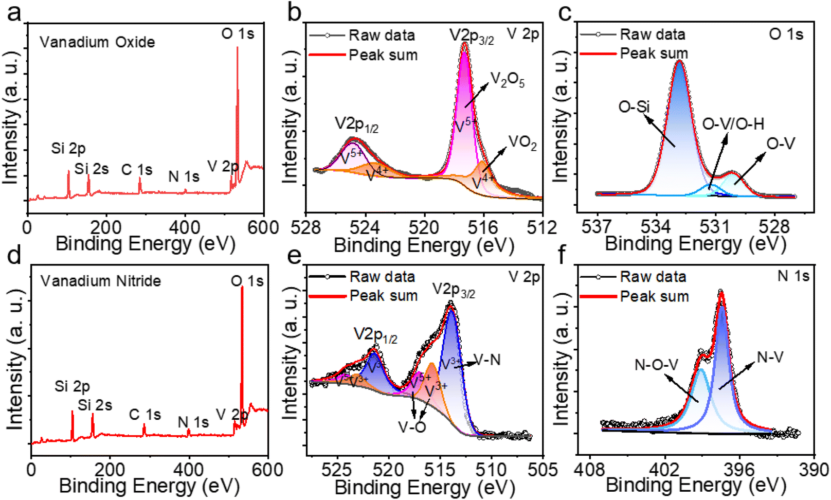 | ||
| Fig. 4 X-ray photoelectron spectroscope (XPS) spectra of the prepared VO2 and VN samples on SiO2/Si substrates showing survey spectrums in (a) and (d). High-resolution, de-convoluted XPS spectra of (b) V 2p and (c) O 1s peaks for vanadium oxide, (e) V 2p and N 1s (f) for vanadium nitride. | ||
Building upon the successful synthesis of two-dimensional vanadium nitride (VN) thin films, we developed a four-electrode device configuration to systematically investigate the thickness-dependent electrical transport properties, specifically focusing on sheet resistance (Rs) and bulk conductivity (σ). Current–voltage characteristics were acquired via voltage measurement under controlled current biasing, with current and voltage explicitly plotted as abscissa and ordinate, respectively, to resolve the electrical transport behavior.
Fig. 5a illustrates the four-probe electrode configuration implemented on a VN thin film. Four Ti/Au electrodes (labeled 1–4) were patterned via electron beam lithography (EBL) and deposited by electron beam evaporation on VN/SiO2/Si substrates. Current (I14) was applied through electrodes 1 and 4 while measuring the voltage drop (V23) between electrodes 2 and 3 under controlled current sweeps (0–100 μA). The channel geometry between electrodes 2 and 3 is defined by length L and width W.
 | ||
| Fig. 5 Impact of thickness to the electrical properties of VN film. (a) A schematic illustration of fabricating a four-electrode configuration on a VN film on SiO2/Si substrate. (b) Room-temperature I–V curves of the samples with different thickness. (c) Plot of Rs versus thickness for VN. | ||
The channel resistance (Rchannel) was calculated as the slope of the linear I14–V23 relationship. This resistance correlates with sheet resistance (Rs) through the relationship:18
 | (1) |
Combining this with the resistivity (ρ) and conductivity (σ) definitions:
 | (2) |
 | (3) |
Sixteen four-electrode VN devices were fabricated and characterized via I–V measurements. Fig. 5b plots the I–V curves for six representative samples with incrementally increasing thicknesses (denoted by distinct line markers), revealing a general decrease in Rchannel (slope of I–V curves) with thicker films. This trend, however, exhibits non-monotonic behavior due to variations in channel geometry (L and W) across devices. Specifically, the 54.5 nm-thick sample demonstrates anomalously higher Rchannel values than the 43.5 nm sample, highlighting the geometric dependence of charge transport (Fig. 5b); and the same for 81.4 and 68.1 nm-thick samples. The linearity of the I–V curves confirms ohmic contact formation at the VN/Ti/Au interfaces and further verifies the metallic nature of the synthesized VN films. This experimental observation aligns with theoretical calculations,33 where analysis of the electronic band structure and density of states (DOS) reveals a gapless ground state and confirms the metallic character of cubic VN.
To quantify intrinsic transport properties, the sheet resistance (Rs) of all 16 devices was calculated from Rchannel (measured L and W) using eqn (1). The comparative analysis of sheet resistance (Rs, y-axis) across varying film thicknesses (x-axis) is presented in the column chart shown in Fig. 5c. As evidenced in the figure, the sheet resistance (Rs) demonstrates a general decreasing trend with increasing film thickness. The observed phenomenon aligned well with the mechanism reported in previous studies,20,34 where improved surface morphology and greater thickness synergistically suppress surface scattering effects, leading to a consequent reduction in sheet resistance. Notably, this dependence deviates from strict monotonicity, which can be predominantly attributed to the presence of incompletely nitrided vanadium oxide species within the thicker film architectures. Furthermore, the electrical conductivity of these devices was calculated using eqn (3), yielding values ranging from 4.25 × 10³ to 1.30 × 10⁴ S cm−1. Notably, this σ value significantly exceeds the reported bulk VN conductivity (0.01538 S cm−1 at room temperature, ρ = 65 Ω cm),35 demonstrating enhanced conductivity in 2D VN nanostructures.
The electrical properties of VO2 were comparatively analyzed (Fig. S3†). Room-temperature I–V measurements revealed near-metallic behavior, likely stabilized by oxygen vacancies generated during high-temperature synthesis, thereby suppressing the insulating phase at 300 K.36 Its sheet resistance (∼103 Ω sq−1) remained two orders of magnitude higher than our VN films. This enhanced conductivity of VN aligns with previous reports as a high-performance conductor.
As summarized in Table S1,† the conductivity of our VN films surpasses those of other 2D transition metal nitrides documented in literature,18,19,37–39 establishing their superior charge transport characteristics.
To systematically verify metallic behavior, a field-effect transistor was fabricated using a VN (31.9 nm) film (Fig. 6a) on 285 nm SiO2/Si substrate, and Si as the back-gate. Gate-voltage sweeps (−40 to 40 V, Vds = 10 mV) demonstrated gate-independent conduction: the drain-source current (Ids, electrodes 2–3) remained constant within noise limits, as quantified in the dashed-line inset of Fig. 6b.
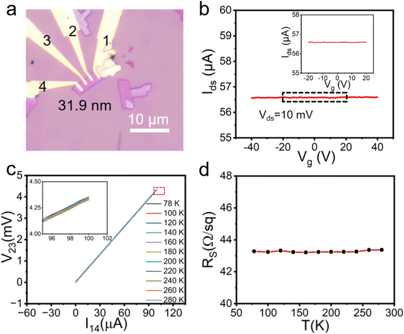 | ||
| Fig. 6 Electrical transport measurements of VN metal properties. (a) Optical image of a back-gate FET device. (b) Transfer curve of VN transport device for both forward and reverse Vg bias with back-gate modulations. Inset: magnified view of the indicated area. Negligible gate dependence of the Ids is observed. (c) Output I14–V23 curves of VN transport device under different temperatures at zero gate voltage. Inset: magnified view of the indicated area. (d) Temperature dependence of the sheet resistance of the VN sample. | ||
Furthermore, temperature-dependent four-probe measurements (77–300 K) were also conducted to verify the electric transport behaviors. The linear I14–V23 curves (Fig. 6c) exhibited negligible slope variation (inset), corresponding to temperature-insensitive sheet resistances (43.2–43.4 Ω sq−1, L = W = 1.5 μm) calculated via eqn (1) (Fig. 6d). The observed temperature-independent sheet resistance (77–300 K) of VN thin films, synthesized via nitridation of VO2 at 650 °C, suggesting that the nitridation process may have altered the original band structure of VO2 to create degenerate states with temperature-stable carrier density.
Experimental
Two-dimensional vanadium nitride (VN) films were fabricated via a two-step chemical vapor deposition (CVD) process
VO2 film transfer
The mica-supported VO2 was sequentially spin-coated with poly (methyl methacrylate) (PMMA; 500 rpm/10 s, and then 2000 rpm/60 s) and polystyrene (PS: 6 g in 50 ml toluene; 500 rpm/10 s, and then 3000 rpm/60 s), followed by thermal curing (PMMA: 130 °C/10 min; PS: 90 °C/10 min). Edge-trimmed substrates were immersed in deionized (DI) water, where mechanical pressure induced water intercalation, enabling polymer-mediated exfoliation. The freestanding VO2/PMMA/PS stack was transferred to SiO2/Si for nitridation or copper TEM grids. Residual polymers were removed by sequential toluene and acetone washes.VN film transfer
VN films on SiO2/Si were spin-coated with PMMA (500 rpm/10 s, and then 2000 rpm/60 s) and cured (130 °C/10 min). After edge removal by blade scraping, the substrate was etched in diluted buffered oxide etch (BOE) to release the PMMA/VN membrane. The floating film was rinsed in DI water (5–10 min) and transferred to TEM grids, followed by PMMA dissolution in acetone.Device fabrication and conductivity measurements
Four-electrode devices were fabricated via electron-beam lithography with Ti/Au electrodes (5/30 nm) deposited by electron-beam evaporation. Temperature-dependent electrical transport properties (77–300 K) were measured using a Keysight B1500A parameter analyzer coupled with a Lakeshore cryogenic probe station under high vacuum (10−4 Pa).Material characterization
The as-prepared samples were characterized using Raman spectroscopy, atomic force microscopy (AFM), transmission electron microscopy (TEM), and X-ray photoelectron spectroscopy (XPS). Raman measurements were conducted using a Horiba Raman microscope equipped with 514 nm laser, 1 μm spot size and 2400 grooves/mm grating. All spectra for comparison were recorded under identical conditions. XPS spectra were obtained using a Thermo Scientific ESCALAB 250Xi with monochromatic Al-Kα (hv = 1486.6 eV) radiation, with a power of 150 W and an X-ray beam spot of 500 μm. And the fixed transmission energy of the energy analyzer is 30 eV. TEM measurements were performed on a JEM-2100 Plus microscope at 200 kV and 0.19 nm point resolution. High-resolution transmission electron microscopy (HRTEM) and energy-dispersive X-ray spectroscopy (EDS) images were acquired using a JEM ARM-200F operated at 200 kV. AFM images were captured with a Bruker Dimension Icon AFM in tapping mode.Conclusions
In summary, two-dimensional cubic-phase vanadium nitride films were successfully synthesized through a chemical vapor deposition-assisted atomic substitution strategy. The smooth surface of synthesized VN films made them suitable for microelectronic devices. Through four-probe testing, studies indicated that the sheet resistance of the prepared VN films decreased with increasing thickness. Furthermore, transfer characteristic analysis unambiguously demonstrated metallic conduction behavior of VN films. Notably, temperature-dependent resistance measurements exhibited remarkable temperature insensitivity within 77–300 K. This temperature-independent sheet resistance characteristic suggested potential applicability in precision electronic systems and functional materials designed for extreme operational conditions, particularly in low-temperature environments. This work provided strong evidence for the preparation of two-dimensional non-layered transition metal nitrides using the atomic substitution method and offered valuable insights and guidance for the study of the electrical transport properties of two-dimensional transition metal nitrides.Data availability
All data needed to support the conclusions in the paper are presented in the manuscript and the ESI.† Additional data related to this paper may be requested from the corresponding author upon request.Author contributions
Q. Y. Y.: conceptualization, methodology, investigation, formal analysis, data curation, validation, writing – original draft preparation, writing – review & editing. Z. P. W.: methodology, investigation, formal analysis, data curation, validation. F. F. S.: investigation. D. H. L.: investigation. Y. P.: investigation. J. Y. L.: investigation. All authors have critically reviewed, provided substantive revisions, and approved the final version of the manuscript.Conflicts of interest
All the contributing authors report no conflict of interests in this work.Acknowledgements
This work was supported by the Scientific Research Foundation of the Higher Education Institutions of Anhui Province, China (Grant No. 2022AH051648, 2024AH040057). We acknowledge the use of DeepSeek's AI-powered language model (https://www.deepseek.com) to assist with text polishing and grammatical refinement in the preparation of this manuscript. The authors take full responsibility for the content and accuracy of the final text.References
- R. S. Ningthoujam and N. S. Gajbhiye, Prog. Mater. Sci., 2015, 70, 50–154 CrossRef CAS.
- R. Adalati, A. Kumar, Y. Kumar and R. Chandra, Energy Technol., 2020, 8, 2000466 CrossRef CAS.
- A. Jrondi, G. Buvat, F. D. L. Pena, M. Marinova, M. Huvé, T. Brousse, P. Roussel and C. Lethien, Adv. Energy Mater., 2023, 13, 2203462 CrossRef CAS.
- S.-Y. Chun, J. Korean Ceram. Soc., 2017, 54, 38–42 CrossRef CAS.
- W. Aperador, J. Duque and E. Delgado, Int. J. Electrochem. Sci., 2016, 11, 4688–4700 CrossRef CAS.
- H. Wang, J. Li, K. Li, Y. Lin, J. Chen, L. Gao, V. Nicolosi, X. Xiao and J.-M. Lee, Chem. Soc. Rev., 2021, 50, 1354–1390 RSC.
- O. Bondarchuk, A. Morel, D. Bélanger, E. Goikolea, T. Brousse and R. Mysyk, J. Power Sources, 2016, 324, 439–446 CrossRef CAS.
- G. Qu, Z. Wang, X. Zhang, S. Zhao, C. Wang, G. Zhao, P. Hou and X. Xu, Chem. Eng. J., 2022, 429, 132406 CrossRef CAS.
- S. Wei, C. Wang, S. Chen, P. Zhang, K. Zhu, C. Wu, P. Song, W. Wen and L. Song, Adv. Energy Mater., 2020, 10, 1903712 CrossRef CAS.
- L. Aissani, M. Fellah, A. H. Chadli, M. A. Samad, A. Cheriet, F. Salhi, C. Nouveau, S. Weiß, A. Obrosov and A. Alhussein, J. Mater. Sci., 2021, 56, 17319–17336 CrossRef CAS.
- A. Kafizas, C. J. Carmalt and I. P. Parkin, Coord. Chem. Rev., 2013, 257, 2073–2119 CrossRef CAS.
- E. Mohimi, Z. V. Zhang, J. L. Mallek, S. Liu, B. B. Trinh, P. P. Shetty, G. S. Girolami and J. R. Abelson, J. Vac. Sci. Technol., A, 2019, 37, 031509 CrossRef.
- A. C. Kozen, M. J. Sowa, L. Ju, N. C. Strandwitz, G. Zeng, T. F. Babuska, Z. Hsain and B. A. Krick, J. Vac. Sci. Technol., A, 2019, 37, 061505 CrossRef.
- C. Zhao, C. Meng, B. Wang, C. Wang, R. Li and Q. Fu, ACS Appl. Nano Mater., 2021, 4, 10735–10742 CrossRef CAS.
- A. K. Geim and K. S. Novoselov, Nat. Mater., 2007, 6(3), 183–191 CrossRef CAS PubMed.
- C. Lan, C. Li, J. C. Ho and Y. Liu, Adv. Electron. Mater., 2020, 7, 2000688 CrossRef.
- Y. Kopelevich and P. Esquinazi, Adv. Mater., 2007, 19(24), 4559–4563 CrossRef CAS.
- H. Gao, J. Cao, T. Li, W. Luo, M. Gray, N. Kumar, K. S. Burch and X. Ling, Chem. Mater., 2021, 34, 351–357 CrossRef.
- H. Gao, D. Zhou, L. Ping, Z. Wang, N. T. Hung, J. Cao, M. Geiwitz, G. Natale, Y. C. Lin, K. S. Burch, R. Saito, M. Terrones and X. Ling, ACS Nano, 2025, 19, 3362–3371 CrossRef CAS PubMed.
- S. Wang, K. Bidinakis, C. Haese, F. H. Hasenburg, O. Yildiz, Z. Ling, S. Frisch, M. Kivala, R. Graf, P. W. M. Blom, S. A. L. Weber, W. Pisula and T. Marszalek, Small, 2023, 19, 2207426 CrossRef CAS.
- F. Ureña-Begara, A. Crunteanu and J.-P. Raskin, Appl. Surf. Sci., 2017, 403, 717–727 CrossRef.
- C. Zhang, Q. Yang, C. Koughia, F. Ye, M. Sanayei, S.-J. Wen and S. Kasap, Thin Solid Films, 2016, 620, 64–69 CrossRef CAS.
- J. Cao, T. Li, H. Gao, Y. Lin, X. Wang, H. Wang, P. Tomas and X. Ling, Sci. Adv., 2020, 6(2), eaax8784 CrossRef CAS PubMed.
- Y. Zhang, Mater. Sci., 2016, 34, 169–176 CAS.
- X. Zhou, H. Chen, D. Shu, C. He and J. Nan, J. Phys. Chem. Solids, 2009, 70, 495–500 CrossRef CAS.
- Z. N. Dai, A. Miyashita, S. Yamamoto, K. Narumi and H. Naramoto, Thin Solid Films, 1999, 347(1–2), 117–120 CrossRef CAS.
- C. Xu, J. Mu, T. Zhou, S. Tian, P. Gao, G. Yin, J. Zhou and F. Li, Adv. Funct. Mater., 2022, 32, 2206501 CrossRef CAS.
- A. Kafizas, G. Hyett and I. P. Parkin, J. Mater. Chem., 2009, 19, 1399–1408 RSC.
- M. Demeter, M. Neumann and W. Reichelt, Surf. Sci., 2000, 454, 41–44 CrossRef.
- W. Xiang, B. Le Drogoff and M. Chaker, Appl. Surf. Sci., 2023, 633, 157607 CrossRef CAS.
- E. F. de Souza, C. A. Chagas, T. C. Ramalho and R. B. de Alencastro, Dalton Trans., 2012, 41, 14381–14390 RSC.
- A. Achour, R. Lucio-Porto, S. Solaymani, M. Islam, I. Ahmad and T. Brousse, J. Mater. Sci.: Mater. Electron., 2018, 29, 13125–13131 CrossRef CAS.
- B. A. Ravan, M. Faghihnasiri and H. Jafari, Mater. Chem. Phys., 2019, 228, 237–243 CrossRef CAS.
- F. Lacy, Nanoscale Res. Lett., 2011, 6, 636 CrossRef PubMed.
- Y. Zhong, X. Xia, F. Shi, J. Zhan, J. Tu and H. J. Fan, Adv. Sci., 2016, 3, 1500286 CrossRef PubMed.
- M. Y. Valakh, V. O. Yukhymchuk, V. M. Dzhagan, O. F. Isaieva, V. S. Yefanov and B. M. Romanyuk, Semicond. Phys. Quantum Electron. Optoelectron., 2024, 27, 136–150 CrossRef CAS.
- P. Urbankowski, B. Anasori, K. Hantanasirisakul, L. Yang, L. Zhang, B. Haines, S. J. May, S. J. L. Billinge and Y. Gogotsi, Nanoscale, 2017, 9, 17722–17730 RSC.
- M. Ritala, M. Leskelä, E. Rauhala and J. Jokinen, J. Electrochem. Soc., 1998, 145(8), 2914–2920 CrossRef CAS.
- S.-K. Chiu, B.-C. Lin, L.-C. Chen, H.-G. Chen, C.-C. Peng and Z.-C. Yang, Surf. Coat. Technol., 2025, 496, 131577 CrossRef CAS.
Footnotes |
| † Electronic supplementary information (ESI) available: Further details of optical images, EDS spectrum, additional electrical measurements and table. See DOI: https://doi.org/10.1039/d5ra03161c |
| ‡ Qiuyun Yang and Ziping Wang contributed equally to this work. |
| This journal is © The Royal Society of Chemistry 2025 |