DOI:
10.1039/D5RA02798E
(Paper)
RSC Adv., 2025,
15, 25929-25939
Enhancing organic solar cell performance via Cu nanorods-doped PEDOT:PSS: a pathway to efficient charge transport and plasmonic enhancement
Received
22nd April 2025
, Accepted 6th July 2025
First published on 21st July 2025
Abstract
Copper nanorods (CuNRs) were synthesized through hydrothermal reduction and used as dopants in the buffer transport layer of polymer solar cells. The CuNRs were incorporated into the hole transport layer of thin-film organic solar cells (TFPSCs) to facilitate charge transport processes. The investigation employs a conventional device architecture for fabricating the solar cells. The results show that the power conversion efficiency (PCE) increased from 3.93% (pristine device) to 5.60% (device with 2% CuNRs), representing an improvement of over 42% compared to the pristine device. The enhanced performance is primarily attributed to the improved localized surface plasmon resonance induced by the CuNRs into the PEDOT:PSS, which enhances charge transport at the interface and reduces charge carrier recombination. In the optimized device with CuNRs doped in the PEDOT:PSS hole transport layer, the highest recorded PCE was 5.60%, demonstrating this approach's effectiveness of the CuNRs in the HTL. The effective use of CuNRs to enhance charge transport and plasmonic effects in thin-film organic solar cells.
1. Introduction
In the past few years, polymer solar cells (PSCs) have garnered significant attention due to their distinct benefits, such as lightweight, mechanical flexibility, ease of fabrication, cost-effectiveness, and tunable optical and electronic properties.1–5 Recently, achieving power conversion efficiencies (PCEs) greater than 20% in bulk heterojunction (BHJ) PSCs has been a major breakthrough in organic photovoltaics.6 This achievement stems from advancements in material development, device optimization, and fabrication methods. However, despite these improvements, PSCs still lag behind high performance inorganic technologies such as CIGS and CdTe, which have reported certified PCEs exceeding 22%.7,8 Emerging materials such as antimony selenosulfide (Sb2(S,Se)3) and kesterite-based CZTS have also shown promising efficiencies in the range of 13–15%, attracting attention due to their earth-abundant, non-toxic composition and stability.9,10 Nonetheless, PSCs face persistent limitations, including insufficient light absorption, limited charge carrier mobility and short exciton diffusion lengths, which continue to hinder further performance enhancement.11–13
PSCs are based on conjugated polymers, with the photoactive layer comprising a combination of donor and acceptor materials. One of the most widely studied donor–acceptor (D/A) systems includes poly(3-hexylthiophene) (P3HT) as the donor and [6,6]-phenyl-C61-butyric acid methyl ester (PCBM) as the acceptor. This active layer is sandwiched between a transparent conductive oxide (TCO) anode and a metallic cathode, usually aluminium (Al), to facilitate charge extraction and transport.14–17 Charge transport layers are integrated at both the anode and cathode interfaces to enhance device performance. These layers are essential for optimizing charge transport, reducing recombination losses, and aligning the energy levels of the device.18 Electron transport layers (ETLs) often include materials such as zinc oxide (ZnO), lithium fluoride (LiF), and titanium dioxide (TiO2), while commonly used hole transport layers (HTLs) consist of poly(3,4-ethylene dioxythiophene) polystyrene sulfonate (PEDOT:PSS), nickel oxide (NiO), and molybdenum trisulfide (MoO3).19–21 Furthermore, the donor and acceptor materials within the active layer create a continuous interpenetrating network, facilitating effective exciton separation and charge transfer. P3HT, in particular, tends to adopt a semi-crystalline structure, strengthening π–π* stacking interactions between polymer chains. This ordered structure improves charge carrier mobility, reduces recombination losses, and contributes to overall device efficiency.22
The performance and long-term stability of PSCs can be significantly enhanced by optimizing the absorber layer composition, refining device architecture, and utilizing advanced interface engineering techniques. One effective approach involves integrating metallic NPs within either the active layer or buffer layers, which has shown to boost both PCE and device stability. Furthermore, incorporating metal NPs enhance light absorption via localized surface plasmonic resonance (LSPR), facilitates charge carrier extraction, and contributes to the controlled morphology of the photoactive layer. Due to their crucial role in enhancing PSC's performance, continued research is necessary to explore innovative NPs synthetic techniques that optimize light harvesting and charge transport, ultimately improving the device's performance and stability of PSCs.23,24 PEDOT:PSS is widely recognized as a standard material for HTL in PSCs due to its excellent transparency, ability to be processed in solution, and compatibility with flexible substrates.25,26 Despite these advantages, several challenges limit its effectiveness and long-term stability in photovoltaic applications. The inherent acidity of PEDOT:PSS, attributed to polystyrene sulfonate, can lead to degradation of adjacent layers, particularly the TCO electrode. Moreover, its relatively low electrical conductivity and poor thermal stability hinder charge transport efficiency, increasing series resistance and reducing PCE. To address these limitations, researchers have explored various doping strategies to enhance the conductivity and stability of PEDOT:PSS. Hamed et al. demonstrated that doping PEDOT:PSS with nickel sulfide (NiS) nanocomposites significantly improved device's performance, achieving a PCE of 6.03%, primarily due to LSPR effects.27 Similarly, in our previous work we introduced copper nanospheres (CuNSs) within the PEDOT:PSS layer, demonstrating that the strong near-field enhancement produced by LSPR significantly improved charge transport and overall device's efficiency (see Table 1).28 Our ETL-free device with architecture ITO/PEDOT:PSS:CuNSs/P3HT:PCBM/Ag resulted in a PCE of 5.44%.
Table 1 Summary of the device performances
| Device structure |
Plasmonic nanostructure |
Voc (V) |
Jsc (mA cm−2) |
FF (%) |
PCE (%) |
Year |
Ref. |
| ITO/PEDOT:PSS-NiSNPs/P3HT:PCBM/LiF/Al |
NiSNPs |
0.58 |
18.65 |
55.88 |
6.03 |
2020 |
27 |
| ITO/ITO/PEDOT:PSS:CuNSs/P3HT:PCBM/Ag |
CuNSs |
0.84 |
10.70 |
93.60 |
5.44 |
2024 |
28 |
| PEDOT:PSS-AuNRs/PTB7:PC71BM/LiF/Al |
AuNRs |
0.80 |
17.90 |
68.80 |
10.31 |
2020 |
29 |
| ITO/PEDOT:PSS:AuNSs:AuNRs/P3HT:PCBM/Al |
AuNRs |
0.63 |
7.95 |
54.00 |
3.65 |
2020 |
30 |
| ITO/PEDOT:PSS-AgNPs/PTB7:PC71BM/Ca/Al |
AgNPs |
0.68 |
14.70 |
63.20 |
6.40 |
2018 |
31 |
| ITO/PEDOT:PSS-CuNW/P3HT:PCBM/Al |
CuNW |
0.58 |
8.78 |
53.00 |
2.80 |
2015 |
32 |
| ITO/PEDOT:PSS:Ag-NPs/PBDB-T:ITIC/PFN/FM |
AgNPs |
0.84 |
15.50 |
49.00 |
6.40 |
2021 |
33 |
| ITO/PEDOT:PSS-ZnO:Ag/P3HT:PCBM/LiF/Al |
ZnO:AgNPs |
0.57 |
16.88 |
50.80 |
4.88 |
2022 |
34 |
1.1 Fundamentals of LSPR effects in energy harvesting
Recent advancements in nanoscience and nanotechnology have led to the exploration of plasmonic metal NPs due to their remarkable optical and electronic properties. Noble metals such as gold (Au), silver (Ag), and copper (Cu) possess a high density of free electrons, which interact strongly with incident electromagnetic waves, giving rise to LSPR effects.35,36 This phenomenon enhances light absorption, scattering, and near-field enhancement, making plasmonic NPs highly beneficial for applications in optoelectronic devices. When exposed to incident photons, collective oscillations of conduction electrons are induced, leading to improved charge carrier dynamics and energy transfer processes within the photoactive layer.37,38
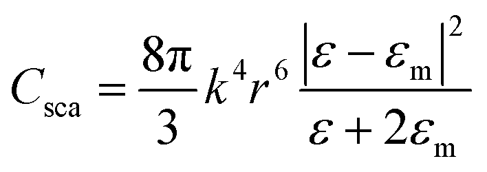
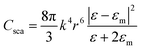
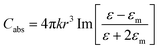
The LSPR effect arises when the dimensions of a metal NP are significantly smaller than the wavelength of incident light, generally under 100 nm. This phenomenon occurs as the oscillating electric field of the incident light triggers collective oscillations of the conduction electrons within the NP, leading to collective electron oscillations. As shown in Fig. 1(a), this interaction results in the polarization of the electron cloud, causing charge separation within the NP.39 Moreover, the accumulation of opposite charges on either side generates an electric dipole, which oscillates in response to the alternating electric field of the incident light. This resonance phenomenon significantly enhances the optical absorption and scattering properties of the NP. Since this resonance is confined to the NP surface, it is termed LSPR. In the case of elongated NPs, such as nanorods (NRs), two distinct resonance modes exist. Longitudinal resonance occurs when electrons oscillate along the longer axis, resulting in absorption in the near-infrared (NIR) region. In contrast, transverse resonance involves oscillations along the shorter axis, leading to absorption in the visible or ultra-violet (UV) spectrum (see Fig. 1(b)). For efficient hot electron generation, NPs must effectively absorb light, leading to photon absorption and the excitation of high-energy electrons above the metal's Fermi level. These energetic electrons can participate in catalytic reactions or contribute to charge transport in photovoltaic applications. The competition between absorption and scattering in plasmonic NPs is primarily influenced by their size, shape, and composition. In spherical NPs, the absorption (Cabs) and scattering (Csca) cross-sections can be mathematically modeled to optimize their behavior for various optoelectronic applications.40,41
| |
 | (1) |
| |
 | (2) |
 |
| | Fig. 1 (a) Schematic depiction of LSPR in metallic NPs via the oscillation of free electrons on the surface of the NPs. (b) Schematic representation of the transverse and longitudinal oscillation of electrons confined in metal NRs. (c) The spectral ranges of metallic NPs with plasmonic properties.42 | |
In this context, the wave vector is given by k = 2π/λ, and λ represents the wavelength of incident light. The particle's radius is denoted as r, while ε and εm correspond to the wavelength-dependent complex permittivity of the metal and the surrounding medium, respectively. Consequently, the condition for plasmon resonance occurs when ε − 2εm = 0, leading to a strong plasmonic absorption band (see Fig. 1(c)).42 As shown in eqn (1) the intrinsic optical properties of the metal nanostructure determine the precise location of this absorption peak.
Different metals exhibit LSPR absorption at distinct spectral regions due to variations in their dielectric properties. For instance, metal nanostructures of noble metals such as Au and Ag typically display strong LSPR effects in the visible to near-infrared region.43 In contrast, metals like magnesium (Mg), indium (In), and gallium (Ga) exhibit LSPR primarily in the UV region.44 While metal sulfides provide tunability and abundance, CuNRs demonstrate stronger LSPR in the visible spectrum, cost less than noble metals, and can be synthesized using wet-chemical methods. These attributes highlight the novelty and potential of CuNRs in enhancing plasmonic effects within OSCs.45,46 These differences arise due to the unique electronic structures and plasmonic behavior of each material. Integrating metal NPs into the buffer layers of PSCs offers several advantages. Metal NPs can serve as conductive bridges, improving charge transport by lowering interfacial resistance. Additionally, different plasmonic effects contribute to enhanced device performance. For instance, LSPR can greatly enhance light absorption in PSCs, by amplifying the interaction between incident photons and the active layer. Furthermore, metal NPs can improve optical confinement by scattering light, effectively increasing the optical path length and boosting absorption efficiency. Moreover, the strong localized electromagnetic fields generated around plasmonic NPs further intensify photon harvesting within the active layer, facilitating enhanced exciton generation and charge separation. These combined mechanisms contribute to improved photovoltaic performance and overall efficiency of PSCs.47–49
In this work, CuNRs were successfully synthesized and incorporated into the PEDOT:PSS matrix through uniform physical mixing, without the need for covalent bonding. Their integration significantly modified the electronic and morphological properties of PE-DOT:PSS, leading to enhanced electrical conductivity, improved carrier mobility, and reduced recombination. The modified PEDOT:PSS was employed as the HTL in P3HT:PCBM-based PSCs, following a conventional device architecture. This strategic incorporation led to a significant enhancement in photovoltaic performance, with an optimized device achieving an average PCE of 5.60% at a CuNRs concentration of 2%. This represents an approximately 42% improvement compared to the reference device without CuNRs. The observed boost in PCE is primarily attributed to enhancements in short-circuit current density (Jsc) and fill factor (FF), both of which contribute to more efficient charge extraction and reduced recombination losses. The findings suggest that embedding CuNRs within the PEDOT:PSS layer effectively improves conductivity and carrier mobility, facilitating better charge transport at the interface.
2. Experimental procedure
2.1 Materials and methods
The polymers utilized in this study included copper sulphate (CuSO4), ascorbic acid (AA), polyvinylpyrrolidone (PVP) with average molecular weight of 40![[thin space (1/6-em)]](https://www.rsc.org/images/entities/char_2009.gif) 000, poly(3,4-ethylene dioxythiophene):poly(styrene sulfonate) (PEDOT:PSS), poly(3-hexylthiophene-2,5-diyl) (P3HT), as well as phenyl-C61-butyric acid methyl ester (PCBM). Additionally, indium tin oxide (ITO)-coated glass substrates measuring 20 × 15 mm with a sheet resistance of 15 Ω per square were acquired from Ossila Co. Ltd.
000, poly(3,4-ethylene dioxythiophene):poly(styrene sulfonate) (PEDOT:PSS), poly(3-hexylthiophene-2,5-diyl) (P3HT), as well as phenyl-C61-butyric acid methyl ester (PCBM). Additionally, indium tin oxide (ITO)-coated glass substrates measuring 20 × 15 mm with a sheet resistance of 15 Ω per square were acquired from Ossila Co. Ltd.
2.2 Synthesis of CuNRs
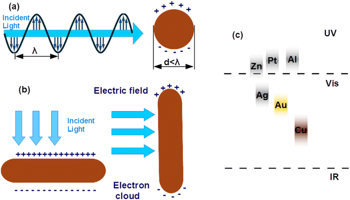
The CuNRs were synthesised by thermal reduction, following the method reported by Zhang et al..50 Briefly, 0.24 g (38.45 mM) of CuSO4, and 0.20 g (45.42 mM) of ascorbic acid were dissolved in 50 ml deionized water (DI H20) and stirred for 5 min. Subsequently, 0.50 g (89.98 mM) of PVP was added to the solution and vigorously stirred to homogeneity. The resulting mixture was transferred into a steel hydrothermal autoclave and heated to 120 °C in an oven for 4 h. A brown colloidal dispersion of CuNRs was obtained, as shown in the insert of Fig. 5(a).
2.3 Fabrication of PSCs
PSCs were fabricated on ITO-coated glass substrates using a conventional device architecture. The substrates underwent a thorough cleaning process, including sequential sonication in DI H20, acetone, and isopropanol for 10 min. After drying with nitrogen, they were annealed at 100 °C for 15 min under ambient conditions. Different volumes (10, 20, and 30 μL) of CuNRs were mixed in 1000 μL of PEDOT:PSS. The PEDOT:PSS doped with and without CuNRs doping was utilized as HTLs that were prepared by spin-coating deposition on ITO substrates at 3500 rpm for 50 s, followed by annealing at 100 °C for 15 min. The absorber layer comprised a blend of P3HT and PCBM, which was prepared by dissolving in chloroform solvent and stirring for 4 h at 50 °C. The P3HT:PCBM precursor solution was spin-coated onto the PEDOT:PSS at 1200 rpm for 45 s and annealed at 100 °C for 10 min. The samples were moved into the vacuum chamber to deposit the ETL (LiF) and Al electrodes. These two were deposited at thicknesses of 14 and 400 nm, respectively. The effective area of each diode has been established as 0.02 cm2. The current density–voltage (J–V) characteristics were measured under standard test conditions using an Ossila solar simulator equipped with a Newport 92251A-1000 solar simulator and an AM 1.5 G filter, providing a light intensity of 100 mW cm−2. The overall device structure consisted of layers in the order: glass/ITO/PEDOT:PSS-CuNRs/P3HT:PCBM/LiF/Al, as illustrated in Fig. 2(a). Correspondingly, Fig. 2(b) presents the energy level alignment across the different functional layers of the fabricated BHJ solar cell device.
 |
| | Fig. 2 (a) Schematic diagram of CuNRs in HTL of PSC and (b) corresponding energy level diagram of the device architecture used in this study. | |
3. Results and discussion
3.1 Characterizations of CuNRs
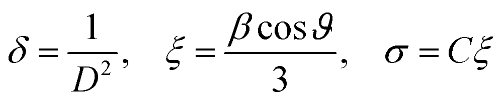
3.1.1 XRD. The X-ray diffraction (XRD) data were measured from CuNRs thin-film shown in Fig. 3. Three prominent peaks are indexed at the diffraction angles 42.87°, 49.98° and 73.79°, corresponding to the (111), (200), and (220) lattice planes, respectively. These peaks confirm the face-centered cubic (FCC) structure of metallic Cu, aligning with the JCPDS No. 04-0836 reference pattern.51 Moreover, the 2θ peak at 42.87° has the highest intensity, indicating preferred orientation along the (111) plane. The crystallite size (D) of the CuNRs was estimated using the Scherrer's equation:| |
 | (3) |
where, λ represents the X-ray wavelength (1.5405 Å), k is the Scherrer's constant (k = 0.89), β represents the full width at half maximum (FWHM) of the diffraction peak in radians, and θ is the Bragg angle. It was found that the crystallite size ranges from 9 to 14 nm, (Table 2), indicating the nanocrystalline nature of CuNRs. This nanoscale crystallinity is advantageous for optoelectronic applications, providing increased surface area and improved electrical conductivity, which are essential for efficient charge transport. Furthermore, structural characteristics such as dislocation density (δ), microstrain (ξ), and stress (σ) were evaluated using the following relationships:| |
 | (4) |
 |
| | Fig. 3 X-ray diffraction pattern of synthesized CuNRs. | |
Table 2 XRD analysis of the obtained CuNRs
| Peak |
2θ (deg) |
β (deg) |
D (nm) |
d-Spacing (nm) |
a (nm) |
δ (10−3 nm−2) |
ξ |
σ (MPa) |
| 111 |
42.861 |
0.867 |
9.737 |
0.211 |
0.365 |
10.55 |
0.201 |
295 |
| 200 |
49.976 |
0.964 |
8.999 |
0.182 |
0.365 |
12.35 |
0.218 |
319 |
| 220 |
74.480 |
0.714 |
13.823 |
0.127 |
0.360 |
5.23 |
0.142 |
207 |
The examined dislocation density of the CuNRs rose as the crystallite sizes diminished. This could be attributed to the decrease in area, which might result from the lack of surface charge properties. Both the microstrain and stress of the CuNRs increase linearly as crystal sizes decrease. Therefore, the lower dislocation density and microstrain typically indicate better crystallinity, which enhances electrical conductivity and charge transport mechanisms in PSCs.
3.1.2 SEM and TEM electron microscopy. Scanning electron microscope (SEM) images of PEDOT:PSS films with and without CuNRs at different concentrations are displayed in Fig. 4(a) and (b). The absence of cracks in the images suggests a uniform polymer coating over the ITO substrate, induced by the viscosity of ethanol amine in PEDOT:PSS. Fig. 4(a) and (b) demonstrate the increasing density of CuNRs as their concentration rises. In addition, the morphology shows well dispersed CuNRs within the polymer matrix, demonstrating an increase in surface roughness, without significant aggregation. This phenomenon enhance optical properties of the HTL.30 Furthermore, the enhanced surface roughness and morphological modifications suggest that CuNRs-doped PEDOT:PSS improves interfacial contact with the active layer, thereby enhancing charge extraction. They predominantly exhibit a rectangular shape with minimal deformation, maintaining a uniform width while varying in length. These observations align with findings reported by Liu et al., who demonstrated a similar morphological structure in uniformly deposited PEDOT:PSS films.29 Fig. 4(c) presents a transmission electron microscope (TEM) image of CuNRs at a resolution of 200 nm, confirming their characteristic rod-like structure. A high aspect ratio of these NRs plays a crucial role in facilitating charge transport, thereby improving device's performance. Additionally, Fig. 4(d) illustrates the Gaussian size distribution of CuNRs in terms of width and length. The CuNRs exhibit an average width of 20.60, 0.54 nm and a length of 57.81, 1.5 nm, making them suitable for integration into PEDOT:PSS thin films. In comparison, Liu et al. incorporated AuNRs ranging from 23–47 nm into PEDOT:PSS to fabricate an ITO/PEDOT:PSS:AuNRs/PTB7-Th:PC71BM/LiF/Al device, achieving a PCE of 10.31%.
 |
| | Fig. 4 SEM images of CuNRs incorporated in PEDOT:PSS for (a) 10 μL and (b) 20 μL, (c) TEM image of CuNRs and (d) Gaussian distribution in terms of (i) width and (ii) length. | |
3.1.3 UV-Vis. The optical characteristics of PSCs incorporating different concentrations of CuNRs within the PEDOT:PSS buffer layer were analyzed using a UV-Vis spectrometer.As shown in Fig. 5(b), the UV-Vis transmission spectra compared pristine and CuNRs-doped PEDOT:PSS films. Notably, the undoped PEDOT:PSS film exhibited a maximum transmittance of 93.3% at 434 nm, indicating its high optical transparency. However, upon incorporating CuNRs, the transmittance decreased to 87.5, 85.2, and 89.6% for 1, 2, and 3% CuNRs-doped samples, respectively. The observed reduction in transmittance can be attributed to the light scattering and absorption effects induced by the CuNRs within PEDOT:PSS. Interestingly, a slight increase in transmittance at 3% CuNRs concentration suggests that excessive CuNRs may lead to agglomeration, thereby reducing the plasmonic enhancement effect. As illustrated in Fig. 5(a), the optical absorption spectrum of the synthesized CuNRs in liquid form, demonstrates a strong absorbance in the visible range with a peak centered around 350 nm and a broad absorption band spanning 300–600 nm. This broad absorption resulted from the LSPR effects associated with the CuNRs. Moreover, Fig. 5(c) presents the UV-Vis absorption spectra of PSCs with PEDOT:PSS buffer layers doped with CuNRs. Among all tested samples, the device incorporating 2% CuNRs exhibited the highest absorption intensity, as evidenced by its distinct peaks. Furthermore, the CuNRs-doped devices displayed enhanced absorption within the 350–450 nm wavelength range, which can be attributed to improved light trapping, multiple scattering effects, and increased photon absorption efficiency. Beyond this range, plasmonic resonance effects further improved absorption in the 800–1000 nm spectral region, suggesting the critical role of CuNRs in the device's optical response. On the other hand, bandgap analysis was done using Tauc plot as depicted in Fig. 5(d). Calculations suggest that the pristine device exhibited a bandgap of 1.47 eV. In contrast, slight reductions were observed in 1 and 2% CuNRs-doped samples, with values of 1.46 and 1.45 eV, respectively. A further decrease in the bandgap for the 3% sample aligns with the absorbance trends observed in Fig. 5(c), indicating a potential correlation between CuNRs' concentration and bandgap modulation.
 |
| | Fig. 5 (a) The absorption spectrum of CuNRs (with insert of colloidal solution of CuNRs) (b) UV-Vis transmission spectra, (c) absorbance spectra, and (d) Tauc plot of PEDOT:PSS with and without CuNRs. | |
3.2 Photovoltaic performance of CuNRs based PSCs
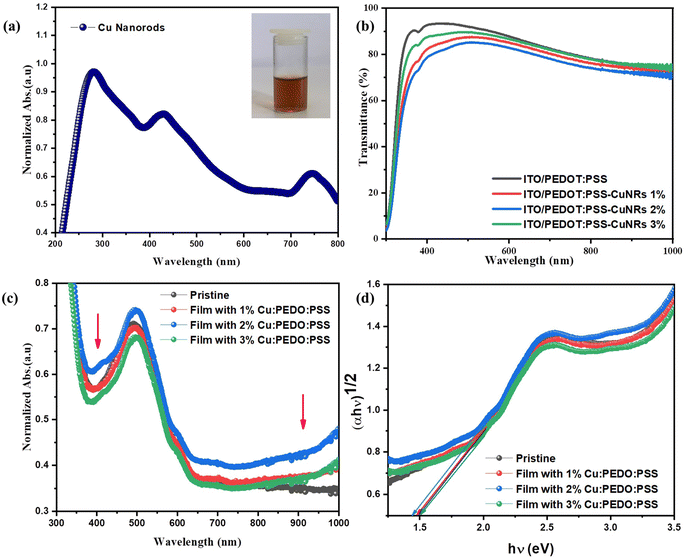
The standard device configuration for PSCs consists of multiple layers, including ITO/PEDOT:PSSCuNRs/P3HT:PCBM/LiF/Al, as depicted in Fig. 2(a). Characterizations of the fabricated devices was conducted using J–V performance analysis, with varying concentrations (1%, 2%, and 3%) of CuNRs in the PEDOT:PSS layer, as shown in Fig. 6(a). Additionally, optical and electrical parameters including the PSC's metrics are summarized in Table 3. For the reference device containing only PEDOT:PSS, the measured parameters were Voc = 0.59 V, Jsc = 11.30 mA cm−2, FF = 58.80%, and PCE = 3.93%. Notably, incorporating CuNRs into PEDOT:PSS led to a significant improvement in device performance. The optimal performance was achieved at a CuNRs' concentration of 2%, yielding a Voc = 0.59 V, Jsc = 15.80 mA cm−2, FF = 59.88%, and improved PCE of 5.60%.
 |
| | Fig. 6 (a) J–V curves of PSCs with and without CuNRs under illumination; (b) J–V characteristics of the corresponding PSCs measured under dark conditions; (c) Jph–Veff curves of devices incorporating different concentrations of CuNRs; and (d) J0.5–V plots under dark conditions. Inset: space-charge limited current (SCLC) fitting using the Mott–Gurney law for pristine and CuNR-incorporated HTLs at varying concentrations. | |
Table 3 Device parameters of PSCs with and without CuNRs in PEDOT:PSS
| CuNRs in the HTL (%) |
Eg |
Eloss (eV) |
Voc (V) |
Jsc (mA cm−2) |
FF (%) |
PCE (%) |
Rs (Ω cm2) |
Rsh (Ω cm2) |
| Pristine |
1.47 |
0.88 |
0.59 |
11.30 |
58.80 |
3.93 |
319.19 |
14953 |
| 1 |
1.46 |
0.86 |
0.60 |
12.90 |
62.65 |
4.85 |
506.40 |
13609 |
| 2 |
1.45 |
0.86 |
0.59 |
15.80 |
59.88 |
5.60 |
223.46 |
10369 |
| 3 |
1.50 |
0.91 |
0.59 |
10.76 |
60.89 |
3.80 |
396.97 |
13555 |
The enhancement in PCE is primarily driven by the increase in Jsc, which rises from 11.30 mA cm−2 in the pristine device to 15.80 mA cm−2 at 2% CuNR doping. This increase is attributed to improved charge transport and extraction at the HTL/active layer interface, facilitated by light scattering and plasmonic effects introduced by the CuNRs. Conversely, a higher concentration of 3% CuNRs resulted in a decline in PCE. This reduction is likely associated with excessive surface roughness, leading to uneven charge transport and increased recombination losses. Furthermore, the series resistance (Rs) and shunt resistance (Rsh) were extracted from the J–V curves and are summarized in Table 3. Among all these samples, the highest Rs was observed in the 1% CuNRs device, indicating greater charge transport resistance. On the other hand, the 2% CuNRs device exhibited a lower Rs signifying enhanced conductivity and reduced resistive losses, depicting improved charge transport. Moreover, a higher Rsh was recorded for both CuNRs-doped and pristine devices, indicating reduced leakage current and better charge selectivity at the electrode interface. This further suggests that incorporating CuNRs into PEDOT:PSS layer improves interfacial properties, ultimately leading to better device stability and efficiency. Furthermore, the energy loss (Eloss) of the device was calculated from the band gap (Eg) using the following equations:
The average Eloss of PSCs is between 0.6 and 1 eV.27
It has been observed that the Eloss of the PSCs produced in this study are within that desired range. Consequently, a 3% device has the highest Eloss of 0.9 eV as compared to the pristine, 1% and 2%, which resulted with decrease in overall performance.
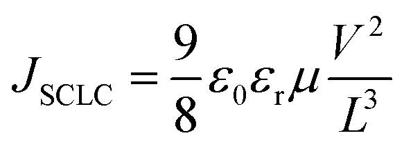
3.2.1 Exciton generation and charge transportation. The relationship between photocurrent density (Jph) and the effective voltage (Veff) is a crucial factor in evaluating exciton dissociation efficiency and charge collection in photovoltaic devices, as shown in Fig. 6(c). Consequently, the Jph versus Veff of all devices with and without PEDOT:PSS were calculated using the below equation:where JL is photo current density and JD is dark current density while the Veff is given bywhere V is the applied voltage and Vo is the compensation voltage at which Jph = 0. The photocurrent density reaches a saturation level (Jsat) when the Veff exceeds 2 V. This suggests that nearly all photogenerated charge carriers are effectively separated, transported, and collected without significant recombination. Based on this assumption, the Jsat primarily relies on the peak exciton generation (G). The G is calculated based on the rate Gmax = Jsat/qL where L represents the thickness of the active layers and q is the elementary charge. However, in the saturation state Veff = 2 V, the Jsat values of pristine are 13.66 mA cm−2, 14.93 mA cm−2 with 1% Cu doped, 18.62 mA cm−2 (1% Cu doped), and 12.44 mA cm−2 (3% Cu doped). This indicates that the device 2% Cu-doped PEDOT:PSS exhibits the highest Gmax of 6.46 × 1024 m−3 S−1, which can enhance the light absorption due to the metal NRs reflecting to increased photon absorption. The exciton dissociation probability by the following equation (ηs = Jpha/Jsat) and charge collection probability (ηc = Jphb/Jsat) can be computed by normalizing Jph concerning saturated Jsat under short circuit and maximal power output conditions, respectively.52–54 The exciton dissociation of the CuNRs doped with PEDOT:PSS was 86%, 84% and 90%, while the original device was 80%. This shows that the doping of the device increases the charge extraction. On the other hand, the charge collection of the devices without additives with CuNRs showed 80, 85, 84 and 86%, respectively. This is due to the enhanced extraction and transport of photogenerated charge carriers.To assess the influence of CuNRs on charge transport in the buffer layer of PSCs, we employed the space-charge-limited current (SCLC) method using the field-dependent mobility equation. This analysis assumes that hole transport is the dominant charge carrier mechanism in the devices. Charge carrier's mobility was determined using the well-known Mott–Gurney equation:
| |
 | (8) |
where
εr is the relative permittivity for organic material (
εr = 3),
ε0 is the permittivity of free space (8.85 10
−12 F cm
−1),
μ is the zero-field mobility,
L is the thickness of the photoactive layer (100 nm), and
V represents the applied voltage corrected for the built-in potential (
Vbi).
55
Consequently, based on the fitting curve in Fig. 6(d) and (inset), the extracted charge mobility values for various devices are summarized in Table 4. PSCs with 2% CuNRs exhibited the highest charge mobility of μ0 = 2.01 × 10⁻³ cm2 s−1 V−1, marking an approximately 80% enhancement compared to the pristine device. This indicates that the optimized CuNRs' concentration significantly improves charge transport efficiency. However, at higher CuNRs concentrations, a decline in mobility was observed. This is likely due to excessive aggregation or phase separation, which disrupts the charge percolation pathways. The improvement in charge mobility can be attributed to enhanced crystallinity in the PEDOT:PSS-CuNRs, which promotes efficient exciton dissociation and charge transfer, ultimately leading to superior device performance.
Table 4 The charge transport parameters of PSCs based on PEDOT:PSS blend with various CuNRs doping levels
| CuNRs (%) |
Jpha (mA cm−2) |
Jphb (mA cm−2) |
Jsat (mA cm−2) |
ηs (%) |
ηc (%) |
Gmax (cm−3 s−1 × 1024) |
μ0 (cm2 s−1 V−1) |
γ (cm V−1) |
| Pristine |
10.96 |
10.94 |
13.66 |
80 |
80 |
4.73 |
1.12 × 10⁻³ |
−1.08 × 10⁻⁴ |
| 1 |
12.90 |
12.82 |
14.93 |
86 |
85 |
5.18 |
2.33 × 10⁻³ |
−2.26 × 10⁻⁴ |
| 2 |
15.80 |
15.74 |
18.62 |
84 |
84 |
6.46 |
2.01 × 10⁻³ |
−1.95 × 10⁻⁴ |
| 3 |
11.30 |
10.72 |
12.44 |
90 |
86 |
4.31 |
4.31 × 10⁻⁴ |
−4.17 × 10⁻⁵ |
4. Conclusion
In summary, CuNRs were successfully synthesized and incorporated into PEDOT:PSS as HTL, effectively enhancing charge transport and conductivity in PSCs. The incorporation of CuNRs led to notable improvements in both the electrical and optical properties of thedevices. At an optimal concentration of 2%, the PCE reached 5.60%, representing a substantial 42% increase compared to the pristine device (PCE = 3.93%). This remarkable enhancement in efficiency can be primarily attributed to the LSPR effect induced by CuNRs, which facilitates charge carrier transport and enhances the conductivity of PEDOT:PSS HTL. Consequently, these results highlight the potential of CuNRs-doped PEDOT:PSS as an effective strategy for improving PSCs performance. Further improvements in PSC's efficiency may be realized by optimizing the CuNRs concentration, refining their morphology, and ensuring uniform dispersion within the HTL. Additionally, the compatibility of CuNRs with roll-to-roll fabrication offers a scalable and cost-efficient approach for large-scale production, paving the way for the development of high-performance PSCs.
Data availability
The data supporting the findings of this study are available within the article. Additional datasets generated and analyzed during the current study are available from the corresponding author upon request.
Conflicts of interest
The authors declare that they have not known any competing financial interests or personal relationships that could have influenced the work reported in this paper.
Acknowledgements
The authors thank the Department of Physics at University of Pretoria and the National Research Foundation with IUD: 115463.
References
- A. Wadsworth, M. Moser, A. Marks, M. S. Little, N. Gasparini, C. J. Brabec, D. Baran and I. McCulloch, Critical review of the molecular design progress in non-fullerene electron acceptors towards commercially viable organic solar cells, Chem. Soc. Rev., 2019, 48(6), 1596–1625 RSC.
- O. Inganäs, Organic photovoltaics over three decades, Adv. Mater., 2018, 30(35), 1800388 CrossRef.
- Y. Cui, H. Yao, J. Zhang, K. Xian, T. Zhang, L. Hong, Y. Wang, Y. Xu, K. Ma, C. An and C. He, Single-junction organic photovoltaic cells with approaching 18% efficiency, Adv. Mater., 2020, 32(19), 1908205 CrossRef CAS PubMed.
- Z. Hu, J. Wang, X. Ma, J. Gao, C. Xu, K. Yang, Z. Wang, J. Zhang and F. Zhang, A critical review on semitransparent organic solar cells, Nano Energy, 2020, 78, 105376 CrossRef CAS.
- J. Gao, W. Gao, X. Ma, Z. Hu, C. Xu, X. Wang, Q. An, C. Yang, X. Zhang and F. Zhang, Over 14.5% efficiency and 71.6% fill factor of ternary organic solar cells with 300 nm thick active layers, Energy Environ. Sci., 2020, 13(3), 958–967 RSC.
- B. Cheng, W. Hou, C. Han, S. Cheng, X. Xia, X. Guo, Y. Li and M. Zhang, Manipulating crystallization kinetics and vertical phase distribution via a small molecule donor guest for organic photovoltaic cells with 20% efficiency, Energy Environ. Sci., 2025, 18(3), 1375–1384 RSC.
- B. Fu, J. Xiong, T. Jv, S. Chen, T. Liang, H. Ma, X. Zhang, D. Pan, B. Zou, G. Liang and D. Ren, Reaction Kinetics Regulation Suppressed Carrier Recombination Loss for High Efficient Solution-Based Antimony Selenosulfide Photovoltaic Devices, Adv. Energy Mater., 2025, 2, 2500586 CrossRef.
- N. Spalatu, M. Krunks and J. Hiie, Structural and optoelectronic properties of CdCl2 activated CdTe thin films modified by multiple thermal annealing, Thin Solid Films, 2017, 633, 106–111 CrossRef CAS.
- B. Shen, T. Zhang, J. Dong, J. Zhang, B. Dong, H. Zhang, S. Jiang, D. Gu, L. Li, S. Zhang and J. Qiu, Heterojunction Interface Anomalous High-Energy Level Insertion Modulating Carrier Dynamics in High-Efficiency Antimony Selenide Thin-Film Solar Cells, Adv. Funct. Mater., 2025, 2503922 CrossRef.
- D. Ren, C. Li, J. Xiong, W. Liang, M. Cathelinaud, X. Zhang, S. Chen, Z. Li, D. Pan, G. Liang and B. Zou, Heterogeneous Nucleation Regulation Amends Unfavorable Crystallization Orientation and Defect Features of Antimony Selenosulfide Film for High-Efficient Planar Solar Cells, Angew. Chem., Int. Ed., 2025, 64(1), e202413108 CrossRef CAS PubMed.
- H. Pan, X. Zhao, X. Gong, H. Li, N. H. Ladi, X. L. Zhang, W. Huang, S. Ahmad, L. Ding, Y. Shen and M. Wang, Advances in design engineering and merits of electron transporting layers in perovskite solar cells, Mater. Horiz., 2020, 7(9), 2276–2291 RSC.
- K. N. Zhang, X. Y. Du, L. Yan, Y. J. Pu, K. Tajima, X. Wang and X. T. Hao, Organic photovoltaic stability: understanding the role of engineering exciton and charge carrier dynamics from recent progress, Small Methods, 2024, 8(2), 2300397 CrossRef CAS PubMed.
- T. Kietzke, Recent advances in organic solar cells, Adv. OptoElectron., 2007, 2007(1), 040285 Search PubMed.
- P. Sonar, J. P. Lim and K. L. Chan, Organic non-fullerene acceptors for organic photovoltaics, Energy Environ. Sci., 2011, 4(5), 1558–1574 RSC.
- Y. J. Cheng, S. H. Yang and C. S. Hsu, Synthesis of conjugated polymers for organic solar cell applications, Chem. Rev., 2009, 109(11), 5868–5923 CrossRef CAS PubMed.
- F. Monestier, J. J. Simon, P. Torchio, L. Escoubas, F. Flory, S. Bailly, R. de Bettignies, S. Guillerez and C. Defranoux, Modeling the short-circuit current density of polymer solar cells based on P3HT: PCBM blend, Sol. Energy Mater. Sol. Cells, 2007, 91(5), 405–410 CrossRef CAS.
- J. M. Méndez-Hernández, A. Hernández-Pérez, M. Oviedo-Mendoza and E. Hernández-Rodríguez, Effects of mechanical deformations on P3HT: PCBM layers for flexible solar cells, Mech. Mater., 2021, 154, 103708 CrossRef.
- P. R. Berger and M. Kim, Polymer solar cells: P3HT:PCBM and beyond, J. Renewable Sustainable Energy, 2018, 10(1), 013508 CrossRef.
- S. Park, S. J. Tark, J. S. Lee, H. Lim and D. Kim, Effects of intrinsic ZnO buffer layer based on P3HT/PCBM organic solar cells with Al-doped ZnO electrode, Sol. Energy Mater. Sol. Cells, 2009, 93(6–7), 1020–1023 CrossRef CAS.
- Q. An, F. Zhang, J. Zhang, W. Tang, Z. Deng and B. Hu, Versatile ternary organic solar cells: a critical review, Energy Environ. Sci., 2016, 9(2), 281–322 RSC.
- Z. Li, Y. Liang, Z. Zhong, J. Qian, G. Liang, K. Zhao, H. Shi, S. Zhong, Y. Yin and W. Tian, A low-work-function, high-conductivity PEDOT: PSS electrode for organic solar cells with a simple structure, Synth. Met., 2015, 210, 363–366 CrossRef CAS.
- R. C. MacKenzie, C. G. Shuttle, M. L. Chabinyc and J. Nelson, Extracting microscopic device parameters from transient photocurrent measurements of P3HT: PCBM solar cells, Adv. Energy Mater., 2012, 2(6), 662–669 CrossRef CAS.
- M. Shaban, M. Benghanem, A. Almohammedi and M. Rabia, Optimization of the active layer P3HT:PCBM for organic solar cell, Coatings, 2021, 11(7), 863 CrossRef CAS.
- A. Y. Ahmed, A. K. Ogundele, M. S. Hamed, N. A. Tegegne, A. Kumar, G. Sharma and G. T. Mola, Application of cobaltsulphide to suppress charge recombinations in polymer solar cell, Mater. Sci. Semicond. Process., 2025, 185, 108917 CrossRef CAS.
- A. Singh, A. Dey and P. K. Iyer, Collective effect of hybrid Au-Ag nanoparticles and organic-inorganic cathode interfacial layers for high performance polymer solar cell, Sol. Energy, 2018, 173, 429–436 CrossRef CAS.
- S. Rafique, S. M. Abdullah, W. E. Mahmoud, A. A. Al-Ghamdi and K. Sulaiman, Stability enhancement in organic solar cells by incorporating V2O5 nanoparticles in the hole transport layer, RSC Adv., 2016, 6(55), 50043–50052 RSC.
- M. S. Hamed, S. O. Oseni, A. Kumar, G. Sharma and G. T. Mola, Nickel sulphide nano-composite assisted hole transport in thin film polymer solar cells, Sol. Energy, 2020, 195, 310–317 CrossRef CAS.
- T. E. Seimela, J. S. Nyarige, N. Nombona and M. Diale, Enhancing the Efficiency of Organic Solar Cell By Incorporating Copper Nanoparticles in PEDOT: PSS. Nano-Horizons, J. Nanosci. Nanotechnol., 2024, 3, 20 Search PubMed.
- Z. Liu, J. Park, B. Li, H. P. Chan, D. K. Yi and E. C. Lee, Performance improvement of organic bulk-heterojunction solar cells using complementary plasmonic gold nanorods, Org. Electron., 2020, 84, 105802 CrossRef CAS.
- S. Phetsang, S. Anuthum, P. Mungkornasawakul, C. Lertvachirapaiboon, R. Ishikawa, K. Shinbo, K. Kato, K. Ounnunkad and A. Baba, Enhancement of organic thin-film solar cells by incorporating hybrid Au nanospheres and Au nanorods on a metallic grating surface, Mol. Cryst. Liq. Cryst., 2020, 705(1), 41–47 CrossRef CAS.
- C. P. Chen, I. C. Lee, Y. Y. Tsai, C. L. Huang, Y. C. Chen and G. W. Huang, Efficient organic solar cells based on PTB7/PC71BM blend film with embedded different shapes silver nanoparticles into PEDOT: PSS as hole transporting layers, Org. Electron., 2018, 62, 95–101 CrossRef CAS.
- J. Chen, W. Zhou, J. Chen, Y. Fan, Z. Zhang, Z. Huang, X. Feng, B. Mi, Y. Ma and W. Huang, Solution-processed copper nanowire flexible transparent electrodes with PEDOT:PSS as binder, protector and oxide-layer scavenger for polymer solar cells, Nano Res., 2015, 8, 1017–1025 CrossRef CAS.
- J. Rivera-Taco, R. Castro-Beltrán, J. L. Maldonado, J. Álvarez-Martínez, D. Barreiro-Argüelles, J. A. Gaspar and G. Gutiérrez-Juárez, The role of silver nanoparticles in the hole transport layer in organic solar cells based on PBDB-T: ITIC, J. Electron. Mater., 2021, 50(7), 4118–4127 CrossRef CAS.
- M. W. Dlamini, X. G. Mbuyise and G. T. Mola, ZnO: Ag nanoparticles decorated hole transport layer for improved photon harvesting, Appl. Phys. A, 2022, 128(2), 125 CrossRef CAS.
- V. Amendola, R. Pilot, M. Frasconi, O. M. Maragó and M. A. Iatí, Surface plasmon resonance in gold nanoparticles: a review, J. Phys.: Condens. Matter, 2017, 29(20), 203002 CrossRef PubMed.
- C. C. Jian, J. Zhang and X. Ma, Cu-Ag alloy for engineering properties and applications based on the LSPR of metal nanoparticles, RSC Adv., 2020, 10(22), 13277–13285 RSC.
- J. Olson, S. Dominguez-Medina, A. Hoggard, L. Y. Wang, W. S. Chang and S. Link, Optical characterization of single plasmonic nanoparticles, Chem. Soc. Rev., 2015, 44(1), 40–57 RSC.
- K. A. Willets and R. P. Van Duyne, Localized surface plasmon resonance spectroscopy and sensing, Annu. Rev. Phys. Chem., 2007, 58(1), 267–297 CrossRef CAS PubMed.
- W. He, X. Huang, X. Ma and J. Zhang, Significant temperature effect on the LSPR properties of noble metal nanoparticles, J. Opt., 2022, 51(1), 142–153 CrossRef.
- Z. Ye, Z. Xu, W. Yue, X. Liu, L. Wang and J. Zhang, Exploiting the LSPR effect for an enhanced photocatalytic hydrogen evolution reaction, Phys. Chem. Chem. Phys., 2023, 25(4), 2706–2716 RSC.
- K. L. Kelly, E. Coronado, L. L. Zhao and G. C. Schatz, The optical properties of metal nanoparticles: the influence of size, shape, and dielectric environment, J. Phys. Chem. B, 2003, 107(3), 668–677 CrossRef CAS.
- J. Zhao, S. Xue, R. Ji, B. Li and J. Li, Localized surface plasmon resonance for enhanced electrocatalysis, Chem. Soc. Rev., 2021, 50(21), 12070–12097 RSC.
- L. Chaabane and I. Trendafilova, Plasmonic nanostructures for enhanced photocatalytic overall water splitting, iScience, 2025, 28(7), 112799 CrossRef PubMed.
- O. Mbrouk, H. R. Galal, W. A. Mohamed, M. S. Abdel-Mottaleb and H. Hafez, Stimulated Photocatalytic Plasmonic–TiO2 Nanohybrid for Ecoremediation and Energy: Recent Advances and Challenges, Energy Technol., 2025, 2401991 CrossRef CAS.
- Y. Xin, K. Yu, L. Zhang, Y. Yang, H. Yuan, H. Li, L. Wang and J. Zeng, Copper-based plasmonic catalysis: recent advances and future perspectives, Adv. Mater., 2021, 33(32), 2008145 CrossRef CAS PubMed.
- R. A. Arishi, A. A. Alghareeb, N. M. Ahmed and S. A. Samsuri, Gold and Copper Nanoparticles Assisted Porous Silicon for high UV Photodetector Sensitivity by Localized Surface Plasmonic Resonance Phenomena, Sens. Actuators, A, 2025, 21, 116595 CrossRef.
- L. M. Liz-Marzán, Tailoring surface plasmons through the morphology and assembly of metal nanoparticles, Langmuir, 2005, 22(1), 32–41 CrossRef PubMed.
- G. T. Mola, M. C. Mthethwa, M. S. Hamed, M. A. Adedeji, X. G. Mbuyise, A. Kumar, G. Sharma and Y. Zang, Local surface plasmon resonance assisted energy harvesting in thin film organic solar cells, J. Alloys Compd., 2021, 856, 158172 CrossRef CAS.
- M. S. Hamed, J. N. Ike, Y. Wang, K. Zhou, W. Ma and G. T. Mola, Reducing Energy Loss in Polymer Solar Cell through Optimization of Novel Metal Nanocomposite, Energy Fuels, 2023, 37(8), 6129–6137 CrossRef CAS.
- X. Zhang, D. Zhang, X. Ni and H. Zheng, One-step preparation of copper nanorods with rectangular cross sections, Solid State Commun., 2006, 139(8), 412–414 CrossRef CAS.
- H. Li, C. Y. Guo and C. L. Xu, A highly sensitive nonenzymatic glucose sensor based on bimetallic Cu–Ag superstructures, Biosens. Bioelectron., 2015, 63, 339–346 CrossRef CAS PubMed.
- D. Hu, Q. Yang, Y. Zheng, H. Tang, S. Chung, R. Singh, J. Lv, J. Fu, Z. Kan, B. Qin and Q. Chen, 15.3% Efficiency All Small-Molecule Organic Solar Cells Achieved by a Locally Asymmetric F, Cl Disubstitution Strategy, Adv. Sci., 2021, 8(8), 2004262 CrossRef CAS PubMed.
- J. D. Chen, C. Cui, Y. Q. Li, L. Zhou, Q. D. Ou, C. Li, Y. Li and J. X. Tang, Single-junction polymer solar cells exceeding 10% power conversion efficiency, Adv. Mater., 2015, 27(6), 1035–1041 CrossRef CAS PubMed.
- T. Zhang, L. C. Winkler, J. Wolansky, J. Schröder, K. Leo and J. Benduhn, High-Performance Filterless Blue Narrow band Organic Photodetectors, Adv. Funct. Mater., 2024, 34(2), 2308719 CrossRef CAS.
- X. Ma, F. Zhang, Q. An, Q. Sun, M. Zhang, J. Miao, Z. Hu and J. Zhang, A liquid crystal material as the third component for ternary polymer solar cells with an efficiency of 10.83% and enhanced stability, J. Mater. Chem. A, 2017, 5(25), 13145–13153 RSC.
|
| This journal is © The Royal Society of Chemistry 2025 |
Click here to see how this site uses Cookies. View our privacy policy here. 
 Open Access Article
 This Open Access Article is licensed under a Creative Commons Attribution-Non Commercial 3.0 Unported Licence
 ,
Mohammed S. G. Hamed
,
Mohammed S. G. Hamed