
 Open Access Article
 This Open Access Article is licensed under a Creative Commons Attribution-Non Commercial 3.0 Unported Licence
Effect of annealing temperature on the electrical properties of IZO TFTs
Zhengang Caiab,
Kamale Tuokedaerhan *ab,
Linyu Yangab,
Zhenhua Huangab,
Chaozhong Guoab,
Raikhan Azamatc and
Yerulan Sagidoldac
*ab,
Linyu Yangab,
Zhenhua Huangab,
Chaozhong Guoab,
Raikhan Azamatc and
Yerulan Sagidoldac
aKey Laboratory of Solid State Physics and Devices, Xinjiang University, Urumqi, Xinjiang 830046, China. E-mail: kamale9025@163.com
bSchool of Physics Science and Technology, Xinjiang University, Urumqi, Xinjiang 830046, China
cDepartment of Solid State Physics and Nonlinear Physics, Faculty of Physics and Technology, AL-Farabi Kazakh National University, 050040 Almaty, Kazakhstan
First published on 16th May 2025
Abstract
The current international demand for thin-film transistors is growing, and reducing the time and economic cost of production while preparing thin-film transistors with excellent electrical properties will have a profound impact on the future development of thin-film transistors. In this paper, we choose the sol–gel method to prepare IZO TFTs, which can reduce the production cost and cycle time by 60% compared with the preparation method that requires vacuum conditions. Since the annealing temperature has a great influence on the electrical properties of IZO TFTs, in this study, we focus on the effect of different annealing temperatures on the electrical properties of IZO TFT devices, and analyze and study the results of the test results of the film structural properties, optical properties, surface morphology, etc. Ultimately, it was found that IZO TFT devices with excellent electrical properties were obtained when the annealing temperature was 350 °C. The turn-off current (Ioff = 2.52 × 10⁻¹³ A), threshold voltage (Vth = 0.8 V), and subthreshold swing (SS = 0.25 V dec−1) were minimized. The highest switching current ratio (Ion/Ioff = 1.58 × 10⁷) and high mobility of 28.71 cm2 V−1 S−1 were achieved. The average transmittance of the films is as high as 98.96%.
1. Introduction
Among the current domestic and international research on oxide semiconductor devices, thin-film transistors (TFTs) have been widely studied for use in electronic devices due to their high mobility and low processing temperatures,1–4 including but not limited to as switching devices in various applications such as sensors, displays, memories, and logic circuits.5 Unlike FET devices,6 TFFs have more advantages in driving active matrix liquid crystal displays (AMLCDs) and active matrix organic light-emitting diodes (AMOLEDs), and have a broad development prospect in the field of flat panel displays.7–10 It has a non-negligible importance for future displays with high resolution, that are foldable, have low power consumption and a large screen.11 Among them, TFTs prepared by indium and zinc elements have good electrical properties, thus they have been widely used in the study of active layers.12–14 As can be seen from Table 1, the comprehensive electrical performance of TFTs prepared from single-element metal oxides is not strong. In contrast, for binary metal oxides, while ensuring that the switching current ratio meets the needs of people's applications (106), and at the same time have a high carrier mobility, the electrical performance of the TFT devices obtained is comprehensively stronger.The first step in the preparation of TFTs is the preparation of oxide semiconductor thin films, and there are many known methods, such as radio-frequency magnetron sputtering (RF MS),15–17 atomic layer deposition (ALD),18–20 pulsed laser deposition (PLD).21–23 Among them, three preparation methods share a common feature, namely, the high requirement of vacuum environment during film preparation, which requires expensive large-scale vacuum equipment to provide protection, and this requirement limits the scale of film preparation and increases the operation difficulty, as well as the time and economic costs.
TFT has a huge application market in the international arena. Facing the vast international market demand, the preparation of thin film transistors with excellent electrical properties while reducing the production time and economic cost will have a far-reaching impact on the future development of thin film transistors.
Compared with the film preparation methods that require vacuum conditions, the sol–gel method has a lower threshold for the preparation of oxide films, which can be prepared directly in air at room temperature, with a 60% reduction in production time and production cost.24 Moreover, it has a simple process, high uniformity, large preparation scale and low cost. In the field of flexible display, whether it is low-cost production or the possibility of large-scale preparation under the premise of ensuring uniformity, or in the study of finished products, due to the simplicity of operation, greatly reducing the threshold of reproduction, further expanding the labor market, its importance to all types of display manufacturers can not be ignored.
Therefore, in this study, InZnO (IZO) TFTs were prepared by sol–gel method, and the hydrolysis condensation reaction rate of the precursor solution was adjusted on-line by physical conditions, and annealed at different annealing temperatures, and the comprehensive electrical properties of the obtained IZO TFTs were not weaker than those of TFT devices prepared under vacuum.
2. Materials and methods
Before making the TFT, the precursor solution should be prepared, the solute in the solvent produces a hydrolytic condensation reaction, first the more polar metal–nitrate precursor loses its chemical bond in solution and ionizes according to eqn (1):24| M(NO3)2·3H2O → M(OH)2 + 2NO3− + H2O + 2H+ | (1) |
| NO3− + 3H+ + 2e− → HNO2 + H2O | (2) |
The metal–nitrate–hydroxide (M–NO3–OH) structure is produced in solution by a condensation reaction as shown in eqn (3) below:24,31
| M(NO3)2·3H2O → M(OH)(NO3)·H2O + HNO3↑ + H2O↑ | (3) |
In the process, the hydrolysis and condensation reactions are carried out simultaneously, and the reaction rates of hydrolysis and condensation should be kept at approximately the same level. Because when the hydrolysis reaction is too fast, due to the high content of alcohol salts within the solution, the hydrolysis reaction is too fast and far exceeds the rate of condensation of the hydrolysis products, leading to precipitation in the solution, so the concentration of the solute should not be too high, because the increase of the concentration of the hydrolysis of the promotion of the hydrolysis is huge, as shown in the accompanying diagram of Fig. 1, in which the solution obtained from the right test tube shows a turbid state white. Several researchers and scholars have chosen to use PTFE to filter precipitates from solutions.32
 | ||
| Fig. 1 Preparation flow of IZO TFTs. | ||
When the rate of condensation is much higher than the rate of hydrolysis, many non-volatile organic compounds will be generated in the solution, which will affect the transmittance of the film and at the same time, produce more air holes in the film in the later annealing process, thus destroying the uniformity and roughness of the film and affecting the electrical properties of the TFT. As shown in the accompanying graph of Fig. 1, this study reasonably modulated the rate of hydrolysis and condensation reactions of solutes in solution and did not produce precipitation.
As shown in Fig. 1 for the preparation process of IZO TFT, firstly, the preparation of InZnO precursor solution was carried out, 0.1 M of zinc nitrate hexahydrate(Zn(NO3)2·6H2O) and 0.1 M of indium nitrate hydrate(In(NO3)3·xH2O)were dissolved in 20 mL of ethylene glycol methyl ether solvent as solutes, and after that the mixture was put into the digital thermostatic magnetic stirring water bath, and stirred for 16 h at a temperature of 50 °C with an appropriate speed (about 500 rpm). Appropriate stirring speed can promote the hydrolysis rate of the solute, and the relative solution temperature of 50 °C can promote the condensation reaction in the solution, under which the hydrolysis and condensation reaction obtained a good equilibrium relationship, and no precipitation appeared in the precursor solution obtained. The short reaction time leads to incomplete hydrolysis and condensation reaction, and excessive stirring will destroy the reaction products, while 16 h is the optimal reaction time for the solution, in which the hydrolysis and condensation reaction is fully reacted and the highest film transmittance is obtained. The obtained solution was aged for 24 h and above to fully stabilize the precursor solution, and finally the IZO precursor solution was obtained.
The substrate used in this paper is n(100) SiO2 with a thickness of 100 nm, and the SiO2 is cleaned before preparing the device by washing it with acetone, alcohol, and deionized water in an ultrasonic cleaner for 10 minutes, respectively. The purpose is to remove organic contaminants, impurity ions, and particulate impurities from the surface of the SiO2 substrate to reduce the factors affecting the device performance.
After that, the precursor solution was spin-coated on SiO2 substrate for TFT device preparation at 3000 rpm for 20 s to obtain IZO films, and the spin-coated films were placed on the substrate at a temperature of 150 °C and heated for 10 min, this operation is to preheat the treatment to achieve the effect of curing the films.
After this cycle of operation for four times to obtain a certain thickness of film, the film is placed in a rapid thermal annealing furnace (RTP) for annealing treatment. The process of heat treatment of the film, the process is accompanied by a large volume contraction and the release of various gases (CO2, H2O, ROH), coupled with the (–OR) base in the non-sufficient oxidation may also be carbonized, leaving carbonaceous particles in the product, so the annealing process should not be too fast. Therefore, in this paper, the films were thermally annealed at different temperatures for 30 min. With the increase of temperature, the metal–nitrate bond was decomposed through the thermal decomposition reaction in eqn (4) and (5), the water in the film was further removed, the remaining nitrate was discharged as gas, and finally a dense metal network was formed within the film.24
| 4M(OH)(NO3)·H2O → 4M(OH)2 + 4NOx↑(5 − 2x)O2↑ + 2H2O↑ | (4) |
| M(OH)2 → MO + H2O↑ | (5) |
Finally, the sputtering of IZO TFT electrode (Al) was carried out in a desktop magnetron sputtering apparatus using the shadow mask method, and the electrode sputtering thickness was about 30 nm. The electrode width W = 100 μm, and the width-to-length ratio W/L = 1/10.
Since the sol–gel method is prepared under the condition of room temperature air, after the IZO TFT is prepared on the same day, it should be encapsulated as soon as possible to avoid prolonged contact with the air, because the active layer will react with some substances in the air, thus affecting the performance of the TFT. In this regard, we have tested, IZO TFT preparation is completed within three days after the package, the device performance is not greatly affected. Therefore, all the IZO TFT devices in this study are tested within three days before packaging.
3. Results and discussion
In order to deepen the understanding of the IZO precursor solution, it was subjected to differential thermal–thermogravimetric analysis (DTA–TGA) and the results obtained are shown in Fig. 2. | ||
| Fig. 2 (a) DTA–TGA curve, (b) DTG–TGA local amplification curve. | ||
The temperature is divided into three stages in the figure, the temperature within 50–148 °C is the first stage; the temperature within 148–350 °C is the second stage; and the temperature within 350–500 °C is the third stage. The three stages have different weight loss, fluctuation of heat absorption and exothermic curves, and weight loss rate, respectively, which are carefully analyzed to further understand the chemical reactions in each process in order to optimize the performance of the TFT devices at a later stage.
From the DTA curve in Fig. 2(a), we can see that 95.11% of the weight loss occurs in the first stage, accompanied by violent fluctuations in the heat absorption and exothermic curves, which is mainly a large amount of evaporation of organic solvents,33 because the evaporation of organic solvents at this stage is too violent, in order to avoid the impact of this process on the top layer of the top film's topographical characteristics, so in the preparation of the TFT device, each layer of the film to be in the preparation of the TFT device, at 150 °C The substrate is heated for 10 min in order to remove most of the solvents therein.
In the second stage, only 0.99% solution weight loss was obtained from the TGA curve, and the fluctuation of the adsorption exothermic curve was soothing, which was due to the desorption of a small amount of physically adsorbed water, the remaining organic solvent and the AcAc complex.33 We investigated the amplification of the corresponding temperature range in the second stage, as shown in Fig. 2(b), there are three fluctuation peaks in the DTG curve, and the starting fluctuation corresponds to the temperatures of 186 °C, 228 °C and 298 °C, respectively. From the literature, it is known that the decomposition temperature of metal ions is inversely proportional to the charge density (CD),34 and the CD of In is about 1.41, and the CD of Zn is about 1.18. Therefore, the decomposition temperature of metal ion In is lower, which is about 184 °C, and the decomposition temperature of metal ion Zn is higher, which is about 233 °C.24 The fluctuation of the differential thermal rate of change curve at 298 °C is due to the fact that at this temperature a dense M–O–M metal network starts to form within the film.
And we found from the DTA curve in Fig. 2(a) that there is a significant heat absorption and exothermic phenomenon in stage III, which is due to the dehydration of absorbed water and the removal of hydroxyl groups (OH−).33 According to the information queried, crystallization of pure IZO films occurs at 540 °C, which is not a fixed temperature, and the crystallization temperature of IZO films decreases with the moisture content within the IZO film, with a minimum crystallization temperature of 280 °C,27,35 while the evaporation of water takes time, and the annealing equipment used in this study is the RTA, which has a short annealing time, therefore, it is presumed that pre-crystallization occurs in the film at stage III, with the presence of grain boundaries within the film, and the tendency of crystallization begins to intensify after 500 °C.
Because crystallization greatly negatively affects the electrical properties of TFTs,36 its crystallization produces grain boundaries, which provide conductive channels for leakage currents in the TFT devices, increasing the device turn-off current and decreasing the switching characteristics of the semiconductors. So the crystallization phenomenon is not the desired result of this study.
In order to verify that the solution prepared in Fig. 2 is an IZO precursor solution, as well as to determine the crystallization temperature of the solution, the samples were subjected to XPS full spectrum as well as XRD tests after being annealed at 400 °C, 500 °C, and 600 °C, respectively, and the results obtained are shown in Fig. 3.
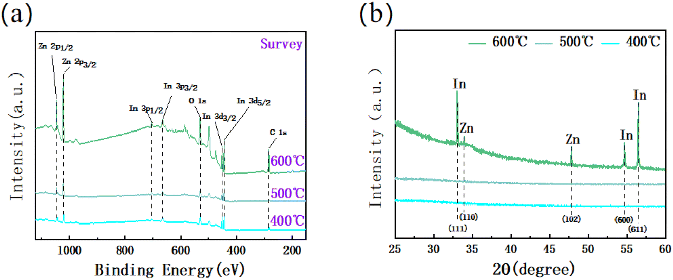 | ||
| Fig. 3 IZO films at annealing temperatures of 400 °C, 500 °C and 600 °C, respectively (a) XPS full spectrum, and (b) XRD curves. | ||
In Fig. 3(a) we can all clearly see that there are corresponding peaks of Zn 2p, In 3d, and O 1s, indicating that the solution obtained from the water bath stirring detected in Fig. 1 is indeed the IZO precursor solution.
We observed a clear crystallization peak on the XRD curve at 600 °C in Fig. 3(b), indicating that significant crystallization was produced at this temperature, but no crystallization peaks were observed on the XRD curves at 400 °C and 500 °C, which may be due to the fact that the crystallization reaction was too weak to be detected.
In order to specify the starting temperature for crystallization and to determine the final annealing temperature, we tested the electrical properties of TFT devices with a 1![[thin space (1/6-em)]](https://www.rsc.org/images/entities/char_2009.gif) :1 ratio of In to Zn annealed at 400 °C, 500 °C, and 600 °C.
:1 ratio of In to Zn annealed at 400 °C, 500 °C, and 600 °C.
Fig. 4(a) shows the nuclear energy level spectra of O 1s orbitals at different annealing temperatures, with VI as the percentage of M–O bonds and VII as the percentage of oxygen vacancies together with OH− ions, because ZnO is found to have an anomalous O 1s spectrum based on XPS knowledge, and the oxygen vacancies corresponding to ZnO are difficult to distinguish from OH−. We find that the percentage of VI gradually elevates and the percentage of VII gradually decreases with increasing annealing temperature, which is attributed to the formation of a dense M–O–M metal network in the film with increasing annealing temperature.
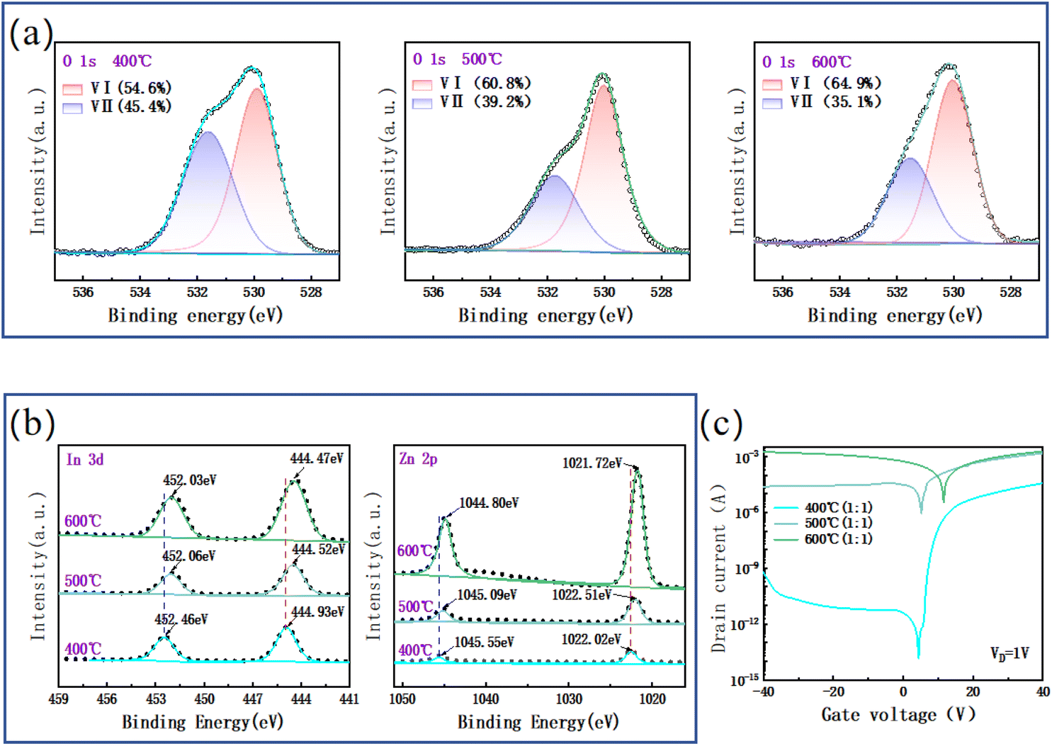 | ||
| Fig. 4 (a) 400 °C, 500 °C and 600 °C O 1s energy spectra, (b) In 3d and Zn 2p XPS spectra, (c) ID–VG curves. | ||
The standard split peak difference between In 3d and Zn 2p is 7.6 eV and 23.0 eV, respectively, which corresponds to the valence states of In and Zn elements of +3 and +2 valence, respectively.37 As shown in Fig. 4(b), at different annealing temperatures, the splitting energy of In 3d is always around 7.55 eV, while the splitting energy of Zn 2p is about 23.04 eV, which indicates that the In–O–Zn metal network is successfully formed within the film after annealing. However, it can be clearly seen from the figure that the nuclear energy level spectra of In and Zn are overall shifted to a low binding energy angle with the increase of annealing temperature, which is due to the energy band shifting phenomenon caused by the continuous electron loss of O2− during the annealing process and its capture by In3+ and Zn2+. The peak of the nuclear energy level spectrum of Zn increases with the annealing temperature, which is due to the fact that XPS is performed on the samples at a depth of 10 nm, whereas at the same temperature ZnO is more active than InO, which is more likely to crystallize, and its crystallization is closer to the upper layers of the film.7,24
Fig. 4(c) shows the electrical data plots of IZO TFTs tested after annealing at 400 °C, 500 °C and 600 °C, respectively, from which it can be seen that, with the same difference in temperature gradient, the electrical performance of the TFT devices annealed at 500 °C is similar to that of the TFT devices annealed at 600 °C, and the difference in the electrical performance of the TFT device samples after annealing at 400 °C is huge. According to Fig. 4(a), it can be seen that with the increase of annealing temperature, the percentage of oxygen vacancies within the film gradually decreases and the defects are reduced, which has a contributing effect on the electrical performance of the film, while the reason why the electrical performance of the annealed samples at 600 °C is so poor is due to the crystallization phenomenon that leads to the emergence of grain boundaries within the film, which provides a conductive channel for the carriers and cavities within the film, resulting in the sharp increase of the leakage current, and the leakage current is increased. The switching characteristics of the TFT device are severely damaged,7 indicating that crystallization has a huge impact on the TFT device. The 500 °C sample did not detect the crystallization peak in Fig. 3(b), then it is because when the annealing temperature is too high, the amorphous film produces new defects with shallow donor energy levels, which are generally regarded as shallow energy level oxygen vacancies, which damage the electrical performance of the device,38,39 while the crystallization temperature of ZnO is not fixed,7 and in this paper, from Fig. 4(b), we observe the elemental Zn The change in the peak value of the nuclear level spectrum, so it does not exclude the possibility that the poorer electrical properties of the 500 °C sample may also be due to the existence of a crystallization trend within the film.
In order to be more certain about the effect of temperature on IZO TFT device performance and to obtain TFTs with better electrical properties, the annealing temperatures of IZO TFTs were reclassified as 300 °C, 350 °C, and 400 °C in this study.
As can be seen from Fig. 5, at the annealing temperature of 400 °C, the AFM 3D map reflects a smoother film overall, with a tiny color change in the AFM 2D map. The smaller thickness of the IZO film in the SEM map indicates that the organic solvent inside the film is gradually excluded as a gas with the increase of the annealing temperature, and the film as a whole becomes denser, but a local sharp protrusion is observed in the AFM 3D map, making the high and low difference of the film reaches 8.8 nm, resulting in a root mean square roughness (RMS) of 0.345 nm from the AFM 2D plot, which is explained by the fluctuation of the DTA curves in Fig. 2(a), without localized sharp protrusions, the root-mean-square roughness of the film at this temperature is 0.214 nm, which conclude that pre-crystallization starts to occur inside the film at 400 °C. While the annealing temperature of 350 °C has no effect of pre-crystallization phenomenon, so the high and low values of the films are 3.9 nm, and the root mean square roughness (RMS) is the lowest of 0.228 nm, and the dense and smooth film without defects is a major key to ensure the excellent electrical properties.
 | ||
| Fig. 5 Detection data of spin-coated films with the same number of layers at different annealing temperatures (a) AFM 3D, and (b) AFM 2D plots, and (c) scanning electron microscope cross-section images. | ||
In order to verify the excellent electrical properties of the 350 °C samples, we tested the electrical properties of IZO TFTs prepared after annealing temperatures of 300 °C, 350 °C, and 400 °C.
From Fig. 6(a), we can clearly see that the turn-off current of the IZO TFT device annealed at 400 °C is obviously the highest, which is consistent with the results obtained from the film characterization in Fig. 5. When the annealing temperature is increased from 300 °C to 350 °C, the DTA curve in Fig. 2(a) is flat and almost no fluctuation, indicating that there is no huge chemical reaction inside the film and the film becomes smooth and defect-free. In the temperature interval from 300 to 400, the carrier concentration inside the film gradually increases, but does not reach the threshold, and the on-state current of the IZO TFT device is improved with the increase of carrier concentration. It is known from the literature that the increase in the concentration of carriers causes a positive shift in the threshold voltage Vth, which is consistent with the electrical results obtained in Fig. 6(a) and 4(c).40 When the IZO TFT sample is annealed at 350 °C, the switching current ratio reaches 107 while the turn-off current is as low as 2.52 × 10⁻¹³ A, which is another order of magnitude lower compared to the sample annealed at 400 °C.
 | ||
| Fig. 6 (a) ID–VG curves of IZO TFTs at different annealing temperatures, (b) ID–VD curves of IZO TFTs at 350 °C, (c) O 1s energy spectra at 350 °C, and different water bath stirring times of IZO precursors, (d) optical bandgap Eg, (e) UV-Vis plots, and (f) structure–function diagram of LEDs. | ||
Fig. 6(b) shows the standard semiconductor device output characteristic curve corresponding to the annealed IZO TFT at 350 °C, which are the curves corresponding to when VG varies in the range 0–35 V, respectively, with a variation of 5 V. Fig. 6(c) shows the O 1s energy spectrum of the film after annealing at 350 °C. VI is lower than that of the annealed sample at 400 °C, which is consistent with the previous conclusion obtained in Fig. 4(a) that the content of oxygen vacancies is inversely proportional to the annealing temperature.
Fig. 6(d–e) shows the optical band gap Eg and film transmittance data of IZO films at different stirring times. The water bath stirring times are 3 h, 8 h, 12 h, 16 h and 20 h, respectively.
The optical band gap Eg is obtained by fitting a linear extrapolation of the Tauc relation41
| αhν = A(hν − Eg)m | (6) |
According to Fig. 6(d), we can know that the maximum value of the optical band gap Eg of the IZO precursor solution is 5.65 eV after stirring in a water bath for 16 h. The larger Eg is, the larger the forbidden bandwidth of the semiconductor is, which is favorable to improve the semiconductor's stability, and it is reasonable to explain why the shutdown current of the IZO TFT device at 350 °C is as high as 10−13 A.
From Fig. 6(e) it can be learned that the longer the stirring time, the higher the transmittance of the IZO films at a water bath temperature of 50 °C and a stirring speed of 500 rpm, the highest transmittance was obtained at a stirring time of 16 h, with an average transmittance of 98.96% which is attributed to the fact that the hydrolysis and condensation in the precursor solution in this time were given a sufficient reaction time.
Fig. 6(f) for the structure of the display LED functional diagram, its working principle is that the light source emits light, through the lower polarizer to filter stray light, the light will be effectively pooled, after which the light passes through the TFT substrate, the liquid crystal layer, the color filter, the upper polarizer output. Light in the process, the direction of travel is always following the liquid crystal, and the electric field controls whether the liquid crystal is rotating, the direction of the upper and lower two polarizers is perpendicular to the direction of light transmission, the light followed by the liquid crystal deflection 90°, you can through the upper polarizer and after the color filter will be a colorful electronic screen presented. Which TFT-LCD specific power consumption of 50–80% depends on the backlight source, which is divided into two parts, part of the luminous efficiency of the LCD luminous body, the other part of the light transmission path needs to be in the light on the effort, in the same light source conditions, to enhance the transmittance of the TFT substrate is one of them. High transmittance IZO precursor solution, reducing the loss of light in the LED transmission process, so that in the case of guaranteeing sufficient screen output brightness, the output of the light source can be reduced, thus greatly reducing the energy consumption of the LED screen. And the high transmittance IZO precursor solution has a greater application prospect in transparent flexible semiconductor devices and human skin release.
Subthreshold swing SS is an important electrical index for TFT devices, and its physical significance lies in the change of VG corresponding to changing ID by one order of magnitude, and smaller SS indicates higher device switching efficiency with the following expression:42
 | (7) |
Carrier mobility μ represents the average drift speed of the carriers under the unit electric field, the higher the mobility, the stronger the conductivity, the faster the positive and negative voltage switching, which is reflected in the electronic display screen with a stronger refresh rate. Its expression is as follows:42
 | (8) |
The gm is the transconductance (gm = dID/dVG). The Cox is the gate capacitance corresponding to 100 nm SiO2.
As can be seen in Fig. 7, the IZO TFT device at 350 °C annealing temperature has the lowest SS and Vth, the low Ioff turn-off current of 2.52 × 10⁻¹³ A, the highest switching current ratio, and the mobility μ of 28.71 cm2 V−1 S−1, which is the best overall electrical performance. The specific data are shown in Table 2.
 | ||
| Fig. 7 Electrical properties at annealing temperatures of 300 °C, 350 °C and 400 °C (a) Vth, SS, and (b) Ioff, and (c) Ion/Ioff μ. | ||
| T (°C) | Vth (V) | SS (V dec−1) | Ioff (A) | Ion/Ioff | μ (cm2 V−1 S−1) |
|---|---|---|---|---|---|
| 300 °C | 0.78 | 0.5 | 1.33 × 10⁻¹³ | 2.49 × 10⁶ | 2.04 |
| 350 °C | 0.8 | 0.25 | 2.52 × 10⁻¹³ | 1.58 × 10⁷ | 28.71 |
| 400 °C | 4.4 | 0.39 | 2.72 × 10⁻¹² | 1.37 × 10⁷ | 33.06 |
Fig. 8(a–c) shows the SEM cross sections of the IZO active layer spin-coated 2, 4, and 6 times at the annealing temperature of 350 °C, respectively. The corresponding film thicknesses are about 45.7 nm, 63.8 nm, and 100 nm, respectively, and in addition to the annealing temperature, the thickness of the active layer also has an important influence on the electrical performance of the TFT devices.
 | ||
| Fig. 8 (a–c)SEM cross-section images of different spin-coating numbers at annealing temperature of 350 °C, and (d) ID–VG curves. | ||
Fig. 8(d) shows the transfer characteristic curves of IZO TFTs detected with different insulating layer thicknesses, from which we can see that the electrical performance of the IZO TFT device with the active layer spin-coated four times is optimal, which is due to the fact that when the thickness of the active layer is relatively thin, the conductive channels formed inside the TFT are narrow and the barrier capacitance is small, and with the increase of the deposition thickness, the quality of the thin film is optimized,43,44 the conductive channel width increases, the electrical performance of the device is improved, and the width of the conductive channel has its threshold, and does not increase with the thickness of the active layer all the time, the optimal thickness of the active layer in 60 nm,45 at this time if the thickness of the active layer is further increased, the electrons will not only be transported in the conductive channel, but also outside of the channel will be the transmission of electrons, the thicker the active layer, the more electrons are transmitted outside the channel, the higher the turn-off current The thicker the active layer is, the more electrons are transmitted outside the channel, and the higher the turn-off current is, the worse the TFT performance is Table 3 shows the statistics of the electrical properties of TFT devices related to indium zinc oxide in recent years, from which it can be seen that the electrical properties of the IZO TFTs obtained in this study using the sol–gel method at an annealing temperature of 350 °C are competitive in terms of different electrical properties compared to the results of this year's studies shown in the table.
| Active layer | Preparation method | Vth (V) | SS (V dec−1) | Ioff (A) | Ion/Ioff | μ (cm2 V−1 S−1) | References |
|---|---|---|---|---|---|---|---|
| InZnO | Sol–gel | — | 2.3 | 10−12 | 104 | 2.03 | 24 |
| InZnLiO | Sol–gel | 0.19 | 0.67 | 10−12 | 106 | 12 | 29 |
| InZnO | PLD | 1.2 | 0.303 | 10−10 | 107 | 20.7 | 32 |
| ZnO | RF MS | 21.4 | 0.9 | 10−11 | 107 | 4 | 45 |
| HfInZnO | RF MS | 0.8 | 0.32 | 10−13 | 107 | 19.2 | 46 |
| InGaZnO | RF MS | 0.8 | 0.25 | 10−13 | 107 | 26.5 | 47 |
| InZnO | Sol–gel | 3 | — | 10−11 | 106 | 7 | 48 |
| InZnO | Sol–gel | 0.8 | 0.25 | 10−13 | 107 | 28.71 | This work |
4. Conclusions
In this paper, IZO TFTs were prepared by sol–gel method. The process stabilized the factors that may affect the device performance such as thickness, water bath time and temperature during the preparation of IZO TFTs. Since the annealing temperature has a large impact on the electrical properties of IZO TFTs, different temperatures of annealing and performance tests were carried out on IZO TFTs, and the data obtained from the tests were analyzed in detail, and the results of the electrical tests and the results of the film characterization were verified with each other, and it was finally found that the IZO TFT devices after annealing at 350 °C had the best overall electrical properties. The turn-off current is 2.52 × 10⁻¹³ A, the threshold voltage is 0.8 V, the subthreshold swing is 0.25 V dec−1, the average transmittance is as high as 98.96%, the switching current ratio is 1.58 × 10⁷, and the mobility is 28.71 cm2 V−1 S−1.Higher transmittance makes it has great application potential in flexible displays, transparent electronic devices, coupled with good electrical properties, which also has a certain use in the bionic electronic skin, higher mobility and lower power consumption, in artificial intelligence has a good application prospect. Most importantly, the sol–gel method used in this study does not require vacuum conditions, which greatly reduces the production cost and production time, in the face of the vast market of thin film transistors, this achievement has the importance of non-negligible. And in the subsequent research, the new IZO/high-k TFT devices prepared by using high dielectric constant materials instead of traditional SiO2 may have more excellent results. Alternatively, nitriding the IZO TFT can enhance its stability.49
Data availability
The data supporting the fundings of this study are available from the corresponding author upon reasonable request.Author contributions
Zhengang Cai: data curation (lead); formal analysis (lead); investigation (lead); methodology (lead); writing – original dra (lead); writing – review & editing (lead). Kamale Tuokedaerhan:supervision (lead); resources (lead); conceptualization (lead); funding acquisition (lead). Linyu Yang: methodology (supporting). Zhenhua Huang: resources (supporting). Chaozhong Guo: resources (supporting). Yerulan Sagidolda: resources (supporting). Zhambyl Azamat: resources (supporting).Conflicts of interest
There are no conflicts to declare.Acknowledgements
This research was supported by the National Natural Science Foundation of China (Grant No. 62141402).References
- H. Jeong, C. S. Kong, S. W. Chang, K. S. Park, S. G. Lee, Y. M. Ha and J. Jang, IEEE Electron Device Lett., 2013, 34, 1569–1571 Search PubMed.
- Y.-S. Park, S. Y. Lee and J.-S. Lee, IEEE Electron Device Lett., 2010, 31, 1134–1136 Search PubMed.
- J. K. Jeong, Semicond. Sci. Technol., 2011, 26, 034008 Search PubMed.
- S. Park, M.-K. Song, T. Sung and J.-Y. Kwon, Appl. Surf. Sci., 2021, 550, 149237 Search PubMed.
- V. Acharya, K. Agarwal and S. Mondal, Mater. Res. Express, 2023, 10, 082002 Search PubMed.
- Z. Zhang, S. Huo, Q. Tian, F. Meng, Z. Yang, Y. Ma, Y. Wang, Y. Xie, X. Hu, W. Gao, E. Wu and C. Pan, Adv. Funct. Mater., 2025, 2424728 Search PubMed.
- W. Xu, H. Li, J.-B. Xu and L. Wang, ACS Appl. Mater. Interfaces, 2018, 10, 25878–25901 Search PubMed.
- X. Yu, T. J. Marks and A. Facchetti, Nat. Mater., 2016, 15, 383–396 Search PubMed.
- A. D. Franklin, Science, 2015, 349, aab2750 Search PubMed.
- C. Glynn and C. O'Dwyer, Adv. Mater. Interfaces, 2017, 4, 1600610 Search PubMed.
- P. Barquinha, G. Gonçalves, L. Pereira, R. Martins and E. Fortunato, Thin Solid Films, 2007, 515, 8450–8454 Search PubMed.
- Y. Hwan Hwang, J.-S. Seo, J. Moon Yun, H. Park, S. Yang, S.-H. Ko Park and B.-S. Bae, NPG Asia Mater., 2013, 5, e45 Search PubMed.
- Y. Liu, K. He, G. Chen, W. R. Leow and X. Chen, Chem. Rev., 2017, 117, 12893–12941 Search PubMed.
- S. Ahmed and J. Yi, Nano–Micro Lett., 2017, 9, 50 Search PubMed.
- S. Arulkumar, S. Parthiban, J. Y. Kwon, Y. Uraoka, J. P. S. Bermundo, A. Mukherjee and B. C. Das, Vacuum, 2022, 199, 110963 Search PubMed.
- K. Ebata, S. Tomai, Y. Tsuruma, T. Iitsuka, S. Matsuzaki and K. Yano, Appl. Phys. Express, 2012, 5, 011102 Search PubMed.
- D. L. Zhu, Q. Wang, S. Han, P. J. Cao, W. J. Liu, F. Jia, Y. X. Zeng, X. C. Ma and Y. M. Lu, Appl. Surf. Sci., 2014, 298, 208–213 Search PubMed.
- Q. Ma, H.-M. Zheng, Y. Shao, B. Zhu, W.-J. Liu, S.-J. Ding and D. W. Zhang, Nanoscale Res. Lett., 2018, 13, 4 Search PubMed.
- J. Sheng, H.-J. Lee, S. Oh and J.-S. Park, ACS Appl. Mater. Interfaces, 2016, 8, 33821–33828 Search PubMed.
- J. Sheng, E. J. Park, B. Shong and J.-S. Park, ACS Appl. Mater. Interfaces, 2017, 9, 23934–23940 Search PubMed.
- M. Gupta, F. R. Chowdhury, D. Barlage and Y. Y. Tsui, Appl. Phys. A, 2013, 110, 793–798 Search PubMed.
- T. Itoh, A. Kobayashi, K. Ueno, J. Ohta and H. Fujioka, Sci. Rep., 2016, 6, 29500 Search PubMed.
- V. H. Martínez-Landeros, N. Hernandez-Como, G. Gutierrez-Heredia, R. Ramírez-Bon, M. A. Quevedo-López and F. S. Aguirre-Tostado, Semicond. Sci. Technol., 2019, 34, 025008 Search PubMed.
- D. Kim, H. Lee, B. Kim, X. Zhang, J.-H. Bae, J.-S. Choi and S. Baang, Materials, 2022, 15, 3416 Search PubMed.
- H. Bong, W. H. Lee, D. Y. Lee, B. J. Kim, J. H. Cho and K. Cho, Appl. Phys. Lett., 2010, 96, 192115 Search PubMed.
- T. Hirao, M. Furuta, T. Hiramatsu, T. Matsuda, C. Li, H. Furuta, H. Hokari, M. Yoshida, H. Ishii and M. Kakegawa, IEEE Trans. Electron Devices, 2008, 55, 3136–3142 Search PubMed.
- J. H. Park, Y. B. Yoo, K. H. Lee, W. S. Jang, J. Y. Oh, S. S. Chae, H. W. Lee, S. W. Han and H. K. Baik, ACS Appl. Mater. Interfaces, 2013, 5, 8067–8075 Search PubMed.
- H.-I. Yeom, J. B. Ko, G. Mun and S.-H. K. Park, J. Mater. Chem. C, 2016, 4, 6873–6880 Search PubMed.
- S. Yue, J. Lu, R. Lu, S. Li, B. Lu, Y. Zhao, X. Li, J. Zhang and Z. Ye, IEEE Trans. Electron Devices, 2019, 66, 2960–2964 Search PubMed.
- Y. Peng, H. Wang, W. Zhang, B. Li, D. Zhou, X. Zhang and Y. Wang, J. Electron. Mater., 2016, 45, 3340–3342 Search PubMed.
- S. Yuvaraj, L. Fan-Yuan, C. Tsong-Huei and Y. Chuin-Tih, J. Phys. Chem. B, 2003, 107, 1044–1047 Search PubMed.
- J. Choi, J. Park, K.-H. Lim, N. Cho, J. Lee, S. Jeon and Y. S. Kim, Appl. Phys. Lett., 2016, 109, 132105 Search PubMed.
- M. M. Islam, J. K. Saha, Md. M. Hasan, J. Kim, R. N. Bukke, A. Ali and J. Jang, Adv. Mater. Interfaces, 2021, 8, 2100600 Search PubMed.
- G. Zhong, S. Xu, C. Chen, D. J. Kline, M. Giroux, Y. Pei, M. Jiao, D. Liu, R. Mi, H. Xie, B. Yang, C. Wang, M. R. Zachariah and L. Hu, Adv. Funct. Mater., 2019, 29, 1904282 Search PubMed.
- A. Steigert, D. Kojda, J. Ibaceta-Jaña, D. Abou-Ras, R. Gunder, N. Alktash, K. Habicht, M. R. Wagner, R. Klenk, S. Raoux, B. Szyszka, I. Lauermann and R. Muydinov, Mater. Today Commun., 2022, 31, 103213 Search PubMed.
- C. Y. Koo, K. Song, T. Jun, D. Kim, Y. Jeong, S.-H. Kim, J. Ha and J. Moon, J. Electrochem. Soc., 2010, 157, J111 Search PubMed.
- H. Lee, J.-H. Kwon, J.-H. Bae, J. Park and C. Seo, J. Nanosci. Nanotechnol., 2019, 19, 2371–2374 Search PubMed.
- S. Hwang, J. H. Lee, C. H. Woo, J. Y. Lee and H. K. Cho, Thin Solid Films, 2011, 519, 5146–5149 Search PubMed.
- Y. Gao, J. Lu, J. Zhang and X. Li, J. Alloys Compd., 2015, 646, 675–679 Search PubMed.
- D. Baek, S.-H. Lee, S.-Y. Bak, H. Jang, J. Lee and M. Yi, Electronics, 2024, 13, 1544 Search PubMed.
- C. Guo, K. Tuokedaerhan, X. Shen, Y. Sagidolda and Z. Azamat, RSC Adv., 2025, 15, 2231–2241 Search PubMed.
- H. Du, K. Tuokedaerhan, R. Zhang, M. Ibraimov and Y. Sagidolda, IEEE Trans. Electron Devices, 2024, 71, 7557–7562 Search PubMed.
- J. H. Ko, I. H. Kim, D. Kim, K. S. Lee, T. S. Lee, B. Cheong and W. M. Kim, Appl. Surf. Sci., 2007, 253, 7398–7403 Search PubMed.
- C. Kim, N.-H. Lee, Y.-K. Kwon and B. Kang, Thin Solid Films, 2013, 544, 129–133 Search PubMed.
- D. Han, L. Huang, W. Yu, Y. Cong, J. Dong, X. Zhang and Y. Wang, IEEE Trans. Electron Devices, 2017, 64, 1997–2000 Search PubMed.
- S.-Y. Han, M.-C. Nguyen, A. H. T. Nguyen, J.-W. Choi, J.-Y. Kim and R. Choi, Thin Solid Films, 2017, 641, 19–23 Search PubMed.
- T. Zhao, C. Zhao, J. Zhang, I. Z. Mitrovic, E. G. Lim, L. Yang, T. Song and C. Zhao, J. Alloys Compd., 2020, 829, 154458 Search PubMed.
- A. Abliz, A. Rusul, H. Duan, A. Maimaiti, L. Yang, M. Zhang and Z. Yang, Chin. J. Phys., 2020, 68, 788–795 Search PubMed.
- Y. Huang, H. Yuan, B. Nie, T. Gong, Y. Wang, S. Lv, P. Jiang, W. Wei, Y. Yang, J. Chai, Z. Wu, X. Wang and Q. Luo, Appl. Phys. Lett., 2024, 124, 133504 Search PubMed.
| This journal is © The Royal Society of Chemistry 2025 |