
 Open Access Article
 This Open Access Article is licensed under a Creative Commons Attribution-Non Commercial 3.0 Unported Licence
Computational and experimental approach for investigating the microstructural parameters of a cadmium indium selenide (α-CdIn2Se4) ternary semiconducting compound
S. D. Dhruva,
Sergei A. Sharkob,
Aleksandra I. Serokurovab,
Nikolai N. Novitskiib,
D. L. Goroshkoc,
Parth Rayanid,
Jagruti Jangalea,
Naveen Agrawala,
Vanaraj Solankif,
J. H. Markna e,
Bharat Katariae and
D. K. Dhruv*a
e,
Bharat Katariae and
D. K. Dhruv*a
aNatubhai V. Patel College of Pure and Applied Sciences, The Charutar Vidya Mandal (CVM) University, Vallabh Vidyanagar 388120, Gujarat, India. E-mail: dhananjaydhruv@rediffmail.com
bLaboratory of Magnetic Films Physics, Scientific-Practical Materials Research Centre of National Academy of Sciences of Belarus, 220072 Minsk, Belarus
cInstitute of Automation and Control Processes Far Eastern Branch of the Russian Academy of Sciences, 5 Radio St., Vladivostok 690041, Russia
dGovernment Science College, Maharaja Krishnakumarsinhji Bhavnagar University, Gariyadhar, Bhavnagar 364505, Gujarat, India
eDepartment of Nanoscience and Advanced Materials, Saurashtra University, Rajkot 360005, Gujarat, India
fDr. K. C. Patel R & D Centre, Charotar University of Science and Technology, Changa 388421, Gujarat, India
First published on 7th May 2025
Abstract
Several properties are carefully considered before choosing a semiconducting material for the fabrication of a thin-film electronic device. Cadmium indium selenide (CdIn2Se4) is a ternary semiconducting compound belonging to the II–III2–VI4 family, where II = zinc (Zn), cadmium (Cd), or mercury (Hg); III = aluminium (Al), gallium (Ga), or indium (In); and VI = sulphur (S), selenium (Se), or tellurium (Te). The Cambridge serial total energy package (CASTEP) module, within the framework of density functional theory (DFT) using the PBE-GGA (Perdew–Burke–Ernzerhof generalized gradient approximation), was used to compute the elastic constants for the CdIn2Se4 ternary semiconducting compound. Stoichiometric amounts of 5 N-pure (99.999%) Cd, In, and Se elements were used to synthesize the CdIn2Se4 compound using a microcontroller-based programmable high-temperature rotary furnace. X-ray diffraction (XRD) was used to examine the crystal structure and phase purity of the synthesized CdIn2Se4 ternary semiconducting compound. The synthesized CdIn2Se4 ternary semiconducting compound exhibited a high level of crystallinity, as evinced by its strong XRD peak intensity and narrow full width at half maximum (FWHM, β) of the diffraction peaks. Identification, indexing, and accurate mapping of the X-ray diffractogram peaks of CdIn2Se4 were successfully performed using ICDD card No. 01-089-2388. The synthesized CdIn2Se4 ternary semiconducting compound possessed a single-phase pseudo-cubic α-phase tetragonal structure (c ≃ a) with the P![[4 with combining macron]](https://www.rsc.org/images/entities/char_0034_0304.gif) 2m(111) crystallographic space group (SG). For the most prominent XRD peak (111), the stacking fault (SF) value of the ternary semiconducting compound CdIn2Se4 was determined to be 1.0267 × 10⁻³. For the preferred orientations of the crystallites along a crystal plane (hkl), the texture coefficient (Ci) of each XRD peak of the ternary semiconducting compound CdIn2Se4 was measured, yielding values close to unity (≃1). The degree of preferred orientation (Δ) for the ternary semiconducting compound CdIn2Se4 was found to be 9.6751 × 10⁻⁴. To gain insight into the growth behavior of the synthesized CdIn2Se4 ternary semiconducting compound, the Bravais theory was applied to compute the d-interplanar spacings (dhkl), enabling inference on the significance of the (111) plane in the crystal structure of CdIn2Se4. The lattice constant (a) for the CdIn2Se4 ternary semiconducting compound was 0.5818 nm, corresponding to a cell volume of 0.1969 nm3, calculated using the Miller indices for the prominent (111) plane. Rietveld refinement (RR) of the XRD data for the ternary semiconducting compound CdIn2Se4 was performed using the FullProf Suite software. Several microstructural parameters of the CdIn2Se4 compound, including lattice parameter (a), crystallite size (D), lattice strain (ε), root mean square strain (εrms), dislocation density (δ), lattice stress (σ), and energy density (u), were determined. Additionally, bulk modulus (BH), shear modulus (GH), Young's modulus (y), Poisson's ratio (ν), elastic anisotropy, melting temperature (Tm), transverse sound velocity (vt), longitudinal sound velocity (vl), average wave velocity (vm), and Debye temperature (θD) were derived for the CdIn2Se4 compound. Energy dispersive X-ray analysis (EDAX) with elemental mapping and a densitometer (pycnometer) confirmed the stoichiometry (with elemental distribution) and density (ρ) of the synthesized CdIn2Se4 compound, respectively. Room temperature (RT) (≃300 K) Fourier transform infrared (FTIR) spectroscopy in the wavenumber (
2m(111) crystallographic space group (SG). For the most prominent XRD peak (111), the stacking fault (SF) value of the ternary semiconducting compound CdIn2Se4 was determined to be 1.0267 × 10⁻³. For the preferred orientations of the crystallites along a crystal plane (hkl), the texture coefficient (Ci) of each XRD peak of the ternary semiconducting compound CdIn2Se4 was measured, yielding values close to unity (≃1). The degree of preferred orientation (Δ) for the ternary semiconducting compound CdIn2Se4 was found to be 9.6751 × 10⁻⁴. To gain insight into the growth behavior of the synthesized CdIn2Se4 ternary semiconducting compound, the Bravais theory was applied to compute the d-interplanar spacings (dhkl), enabling inference on the significance of the (111) plane in the crystal structure of CdIn2Se4. The lattice constant (a) for the CdIn2Se4 ternary semiconducting compound was 0.5818 nm, corresponding to a cell volume of 0.1969 nm3, calculated using the Miller indices for the prominent (111) plane. Rietveld refinement (RR) of the XRD data for the ternary semiconducting compound CdIn2Se4 was performed using the FullProf Suite software. Several microstructural parameters of the CdIn2Se4 compound, including lattice parameter (a), crystallite size (D), lattice strain (ε), root mean square strain (εrms), dislocation density (δ), lattice stress (σ), and energy density (u), were determined. Additionally, bulk modulus (BH), shear modulus (GH), Young's modulus (y), Poisson's ratio (ν), elastic anisotropy, melting temperature (Tm), transverse sound velocity (vt), longitudinal sound velocity (vl), average wave velocity (vm), and Debye temperature (θD) were derived for the CdIn2Se4 compound. Energy dispersive X-ray analysis (EDAX) with elemental mapping and a densitometer (pycnometer) confirmed the stoichiometry (with elemental distribution) and density (ρ) of the synthesized CdIn2Se4 compound, respectively. Room temperature (RT) (≃300 K) Fourier transform infrared (FTIR) spectroscopy in the wavenumber (![[small nu, Greek, macron]](https://www.rsc.org/images/entities/i_char_e0ce.gif) ) range of 4000–400 cm−1 confirmed the purity of the synthesized CdIn2Se4 ternary semiconducting compound by detecting the presence of functional group/s, if any, in the FTIR spectra. The findings obtained from the detailed investigation of the CdIn2Se4 compound may serve as a valuable reference for future researchers focused on device development. Accordingly, the authors have made a concerted effort to examine various properties of the CdIn2Se4 ternary semiconducting compound through both theoretical and experimental approaches. It is anticipated that researchers worldwide may utilize these results in the development of a wide range of electronic devices. The implications of the study are discussed.
) range of 4000–400 cm−1 confirmed the purity of the synthesized CdIn2Se4 ternary semiconducting compound by detecting the presence of functional group/s, if any, in the FTIR spectra. The findings obtained from the detailed investigation of the CdIn2Se4 compound may serve as a valuable reference for future researchers focused on device development. Accordingly, the authors have made a concerted effort to examine various properties of the CdIn2Se4 ternary semiconducting compound through both theoretical and experimental approaches. It is anticipated that researchers worldwide may utilize these results in the development of a wide range of electronic devices. The implications of the study are discussed.
1. Introduction
A review of the literature on the synthesis of II–III2–VI4 ternary semiconducting compounds (where II = zinc (Zn), cadmium (Cd), or mercury (Hg); III = aluminium (Al), gallium (Ga), or indium (In); VI = sulphur (S), selenium (Se), or tellurium (Te)) reveals that many researchers have investigated the growth of II–III2–VI4 compounds using numerous techniques. These include the fusion of II, III, and VI group elements (FC) or binary II–VI and III2–VI3 compounds (FBC), chemical transport reactions (CTRs), growth from the melt (GM), zone melting (ZM), and others.1–5 These materials are considered promising for optoelectronic devices,6–8 memory switching devices,9,10 and more.A polycrystalline ingot of cadmium indium selenide (CdIn2Se4) was prepared by the direct fusion of stoichiometric amounts of their constituting elements cadmium (Cd), indium (In), and selenium (Se) by Tomkiewicz et al.11 The binary component of CdSe and In2Se3 in stoichiometric proportions was used by El-Zaidia et al.2 and El-Nahass et al.12 to prepare a CdIn2Se4 bulk by the direct fusion method. Stoichiometric single crystals of tetragonal (pseudo-cubic) CdIn2Se4 were grown by the chemical vapour transport (CVT) method using iodine as a transport agent by Santamaría-Pérez et al.,3 Neumann et al.,13,14 Razzetti et al.,15 Fornarini et al.,16 Trykozko et al.,17 Margaritondo et al.,18 and Przedmojski et al.19 Adpakpang et al.20 have synthesized a CdIn2Se4 powder via aqueous chemical reduction (solution method). Ruanthon et al.21 have prepared a CdIn2Se4 compound by a sol–gel method. Choe et al.22 and Kerimova et al.23 have grown CdIn2Se4 single crystals by the vertical Bridgman technique. Guerrero et al.24 have grown the CdIn2Se4 compound by a melt-and-anneal technique. Fortin et al.25 and Nitsche et al.26 have grown CdIn2Se4 compounds by chemical transport.
Bulk modulus, elastic constants, and force constants of interatomic bonds of II–III2–VI4 compounds were scrutinized by Mamedova et al.27 and Chandra et al.28 by using ab initio density functional perturbation theory. Priyambada et al.29 and Hoat et al.30 have explored the exhaustive structural, electronic, elastic, mechanical, and thermoelectric chattels of defect CdIn2Se4 chalcopyrite-type semiconductor using an ab initio slant within the density functional theory (DFT) along with the semi-classical Boltzmann transport theory. The results obtained by Hoat et al.30 reveal that CdIn2Se4 is a promising absorber to work under ultraviolet radiation, and thermoelectric parameters such as Seebeck coefficient, electrical conductivity, electronic thermal conductivity, power factor, and dimensionless figure of merit were estimated. Only Santamaria-Perez et al.3 have steered both experimental and theoretical studies on CdIn2Se4 and presented the structural and vibrational properties of CdIn2Se4 under high pressure at ambient temperature.
Ternary semiconducting compound CdIn2Se4 has engrossed much contemplation from researchers due to its claims in heterojunction solar cells,31 photoanodes,32 photoelectrochemical solar cells,11,16,33–35 thermoelectric materials,20,21 photovoltaics,36 etc.
No crystal can be regarded as perfect due to its intrinsic restrictions; a perfect crystal would seem to extend indefinitely in all directions. Diffraction peak broadening is instigated by changes in materials that preserve crystallinity. The primary measurements obtained from the peak width analysis of X-ray diffraction (XRD) are crystallite size (D) and lattice strain (ε).
The extant research paper throws light on the synthesis of CdIn2Se4 ternary semiconducting compounds by melting 5 N (99.999%) pure cadmium (Cd), indium (In), and selenium (Se) constituent elements in stoichiometric proportions. The investigation determines crystallographic characteristics such as stacking faults (SF), texture coefficient (Ci), degree of preferred orientation (Δ), lattice parameters (a, b, and c), and unit cell volume (V) for the CdIn2Se4 ternary semiconducting compound. Various microstructural parameters such as crystallite size (D), lattice strain (ε), root mean square strain (εrms), dislocation density (δ), lattice stress (σ), and energy density (u) of this compound have been derived by employing the Nelson–Riley (N–R), Scherrer, Stokes–Wilson (S–W), Monshi, Williamson–Smallman (W–S), Williamson–Hall (W–H), size–strain plot (SSP), and Halder–Wagner (H–W) methods. Bulk modulus (BH), shear modulus (GH), Young's modulus (y), Poisson's ratio (ν), elastic anisotropy, melting temperature (Tm), transverse sound velocity (vt), longitudinal sound velocity (vl), average wave velocity (vm), and Debye temperature (θD) have also been derived for this compound. Energy dispersive X-ray analysis (EDAX) and a densitometer (pycnometer) have verified the stoichiometry and density (ρ) of the synthesized CdIn2Se4 ternary semiconducting compound, respectively, while Fourier transform infrared (FTIR) spectroscopy has confirmed the compound's purity.
Several of the material's qualities are well-thought-out before picking a semiconducting material to construct a thin-film semiconductor electronic gizmo. Thus, the data salvaged from the CdIn2Se4 ternary semiconducting compound's detailed studies may obligate future device development investigators. The authors, hence, tried to meticulously scrutinize the different properties of the CdIn2Se4 ternary semiconducting compound theoretically and experimentally; it is expected that researchers worldwide will use the findings for the fabrication of various devices.
2. Experimental
2.1. Computational details
The elastic constant calculations for the CdIn2Se4 ternary semiconducting compound were performed using the Cambridge serial total energy package (CASTEP, a package for performing ab initio quantum-mechanical atomistic simulations) module in the density functional theory (DFT) framework under the Perdew–Burke–Ernzerhof-generalized gradient approximation (PBE-GGA) approach.37 The CASTEP calculation was performed with single-point energy calculation using the Perdew–Burke–Ernzerhof (PBE) exchange–correlation functional without spin polarization. The cut-off energy for the plane-wave basis set was set to 394.6000 eV, ensuring sufficient accuracy in the electronic structure calculations. The k-points were explicitly defined using the KPOINTS_LIST rather than an automatically generated grid. A total of 15 k-points were sampled in the Brillouin zone, with representative points such as (0.3333, 0.3333, 0.3333) and (0.3333, 0.3333, 0.0000), each assigned a weight of 0.0741. The self-consistent field (SCF) energy convergence tolerance was set to 1.0000 × 10⁻⁶ eV, with a maximum of 100 self-consistent field (SCF) cycles allowed. The Pulay mixing scheme was used for charge density mixing, with a mixing amplitude of 0.5, a mixing Gmax of 1.5, and a mixing history length of 20 iterations. For metallic systems, the density mixing (DM) method was employed. If geometry optimizations were included, the limited-memory Broyden–Fletcher–Goldfarb–Shanno (L-BFGS or LM-BFGS) method would be used with convergence criteria of 1.0000 × 10⁻⁵ eV for energy, 0.0300 eV Å−1 for force, 0.0500 GPa for stress, and 1.0000 × 10⁻³ Å for displacement, with a maximum of 100 iterations.The elastic constant's calculations employed the stress–strain method, a widely accepted approach for determining elastic properties; this method systematically applied a series of small deformations (strains) to the crystal lattice, and the resulting stress responses were recorded. The CAmbridge Serial Total Energy Package (CASTEP) simulation involved the application of different strain patterns, each corresponding to specific components of the elastic stiffness tensor (Cij). The corresponding stress tensor was computed using the Hellmann–Feynman theorem for each applied strain, ensuring an accurate representation of the CdIn2Se4 ternary semiconducting compound's elastic behaviour. The calculated stress components were then used to extract the elastic constants using a least-squares fitting method, which minimizes errors in the obtained values. The calculations were performed under high-precision settings to ensure numerical accuracy and convergence, including an appropriately chosen plane-wave cut-off energy and k-point sampling based on the Monkhorst–Pack scheme. The transformed stress tensors were recorded for multiple strain amplitudes, allowing for a robust evaluation of the elastic coefficients of the α-CdIn2Se4 ternary semiconducting compound. The elastic coefficients' computed values were further analyzed to obtain secondary mechanical properties such as Bulk modulus (BH), shear modulus (GH), Young's modulus (y), Poisson's ratio (ν), elastic anisotropy, melting temperature (Tm), transverse sound velocity (vt), longitudinal sound velocity (vl), average wave velocity (vm), and Debye temperature (θD), which provides insights into the mechanical stability of the α-CdIn2Se4 ternary semiconducting compound material and its potential applicability in developing various applications in science and technology. The formation energy of the α-(phase) CdIn2Se4 ternary semiconducting compound is −4.1118 eV per formula unit; the negative sign indicates that the synthesized α-(phase) CdIn2Se4 ternary semiconducting compound is stable and thermodynamically favourable.
The authors used the bond lengths, bond angles, and atom parameters of the ternary semiconducting compound CdIn2Se4, which were obtained using Rietveld refinement to calculate the elastic constants. The elastic stiffness constants (Cij) for the ternary semiconducting compound CdIn2Se4 deduced using the CAmbridge Serial Total Energy Package (CASTEP) simulation tool are listed in Table 1.
| Elastic stiffness constants (Cij) (GPa) | α-CdIn2Se4 | β-CdIn2Se4 (ref. 29) |
|---|---|---|
| C11 | 59.7039 | 28.7910 |
| C12 | 41.3956 | 10.8900 |
| C13 | 32.9847 | 12.1850 |
| C33 | 43.5708 | 29.3700 |
| C44 | 20.6089 | 20.2880 |
| C55 | 20.6089 | — |
| C66 | 26.0705 | 20.2770 |
The values of various elastic stiffness constants (Cij) of ternary semiconducting compound CdIn2Se4 derive elastic compliance constants (Sij) 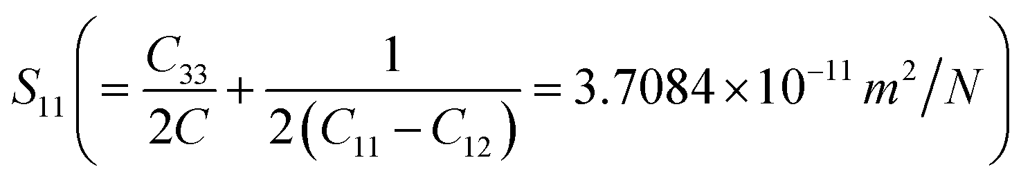 ,
, 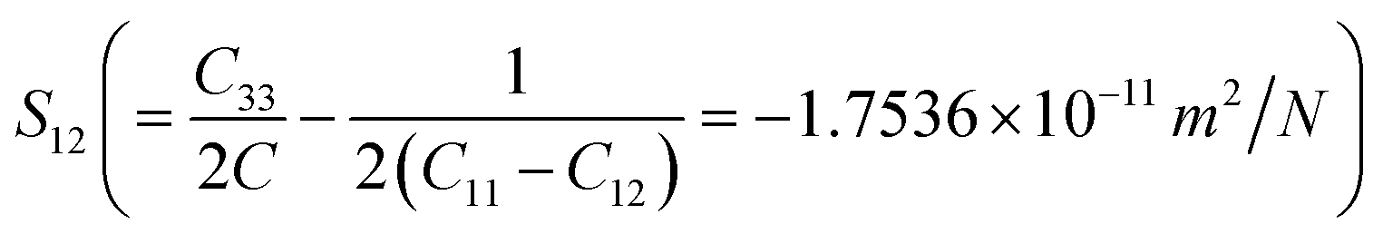 ,
, 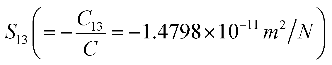 ,
,  ,
,  ,
,  , and
, and  .
.
To confirm the mechanical stability of the tetragonal crystal system, the values of elastic stiffness constants (Cij) should satisfy the conditions C11 (=59.7039 GPa) > 0, C33 (=43.5708 GPa) > 0, C44 (=20.6089 GPa) > 0, C66 (=26.0705 GPa) > 0, C11 (=59.7039 GPa) > C12 (=41.3956 GPa), C11 + C33 – 2C13 (=37.3054 GPa) > 0, and 2C11 + C33 + 2C12 + 4C13 (=377.7082 GPa) > 0, suggested by the Born–Huang lattice dynamical theory,38 which is satisfied well by the ternary semiconducting compound CdIn2Se4 (the values are written in brackets), confirming the mechanical stability of the tetragonal ternary semiconducting compound CdIn2Se4 system.
2.2. Materials and methods
) range of 4000–400 cm−1 to perceive the functional group/s (if any) extant in the synthesized CdIn2Se4 bulk.3. Results and discussion
3.1. X-ray diffraction (XRD) analysis
The CdIn2Se4 ternary semiconducting compound's synthesis was investigated using room temperature (RT) (≃300 K) X-ray diffraction (XRD) analysis. Fig. 1 illustrates the powder X-ray diffractogram of the CdIn2Se4 ternary semiconducting compound with the histogram (in red) screening standard data (ICDD card 01-089-2388). The pragmatic diffraction pattern accords pleasingly with the standard ICDD data. The strong diffraction peak at 26.5277° 2θ along with the other major diffraction peaks at 21.5954° 34.4587°, 37.8671°, 44.0075°, and 52.1227° agreeing to the (111), (101), (201), (112), (202), and (113) reflection planes stretches the signature for the establishment of the untainted CdIn2Se4 system [ICDD card 01-089-2388]. High levels of crystallinity are opined by a potent X-ray diffraction (XRD) peak intensity and a modest full width at half maximum (FWHM) value in the synthesized CdIn2Se4 ternary semiconducting compound. Three phases of tetragonal CdIn2Se4 (α, β, and γ) are distinguished by their c/a ratio value. The c/a ratio is 1 in α-(phase), 2 in β-(phase), and 4 in γ-(phase) CdIn2Se4. Since the c/a ratio in the α-phase of tetragonal CdIn2Se4 is 1, giving the appearance that the system is cubic, it is also referred to as a pseudo-cubic crystal system. According to ICDD card 01-089-2388, the α-(phase) CdIn2Se4 ternary semiconducting compound has a single-phase tetragonal (pseudo-cubic) (c ≃ a) structure and crystallographic space group (SG) P2m(111).30 The most prevalent structure of CdIn2Se4 is tetragonal α-phase, where two Cd ions, one In ion, and one vacancy coordinate each cation tetrahedrally. The high-intensity mountaintops of X-ray diffraction (XRD), i.e., (111), (201), (202), and (113), have been employed for exhaustive scrutiny throughout the study.
 | ||
| Fig. 1 X-ray diffractogram of the ternary semiconducting compound CdIn2Se4. | ||
To learn the d-interplanar spacings, the diffraction angle (2θ) of each reflection is measured, and the protuberant Bragg's relation is applied (eqn (1)):41
nλ = 2d![[thin space (1/6-em)]](https://www.rsc.org/images/entities/char_2009.gif) sinθ sinθ
| (1) |
Table 2 equivalences the d-interplanar spacings found for each reflection to the facts found by Hahn et al.42
| h | k | l | 2θ (°) | Intensity (a.u.) | d-interplanar spacing values (nm) | SF (×10−3) | Ci | ||
|---|---|---|---|---|---|---|---|---|---|
| Reporteda | Calculatedb | Calculatedc | |||||||
| a ICDD card 01-089-2388.b X-ray diffraction (XRD) pattern of the bulk (using Bragg's law).c Bravais theory. | |||||||||
| 1 | 1 | 1 | 26.5277 | 100.0000 | 0.3357 | 0.3358 | 0.3359 | 1.0267 | 1.0003 |
| 2 | 0 | 1 | 34.4587 | 017.3729 | 0.2601 | 0.2601 | 0.2602 | 0.9057 | 0.9987 |
| 2 | 0 | 2 | 44.0075 | 058.7663 | 0.2056 | 0.2057 | 0.2057 | 0.7958 | 0.9997 |
| 1 | 1 | 3 | 52.1227 | 030.9344 | 0.1753 | 0.1754 | 0.1754 | 0.7300 | 1.0014 |
Stacking faults (SF) are defects in crystallography that designate the ineptness of crystallographic planes and are thus stared as planar defects (2D). The stacking fault (SF) morals of un-doped CdIn2Se4 for four intense peaks [(111), (201), (202), and (113)] are intended using eqn (2) and presented in Table 2,43
 | (2) |
In the above relation, β is the measure of full breadth/width at half maximum (FWHM) of the diffraction peak.
Exploiting eqn (3), one can discern the crystallites' preferred orientation along a crystal plane (hkl) by gauging the texture coefficient (Ci) of each X-ray diffraction (XRD) peak,44
 | (3) |
In this context, Ci denotes the texture coefficient of plane i, Ii denotes the leisurely integral intensity, Ii0 denotes the integral intensity of the reported data (ICDD powder diffraction pattern) of the comparable peak i, and N, which is equal to four (=4) in the current study, denotes the number of reflections in the X-ray diffraction (XRD) pattern utilized for analysis. The value of texture coefficient (Ci) is unity (≃1) for each reflection in the case of a capriciously oriented sample; grander than unity (>1), it designates the favored orientation of the crystallites in that specific direction.45 The texture coefficient (Ci) of all four significant peaks [(111), (201), (202), and (113)] for the CdIn2Se4 ternary semiconducting compound are accessible in Table 2.
The degree of preferred orientation (Δ) of the CdIn2Se4 ternary semiconducting compound can be adjudicated by reckoning the standard deviation of all the texture coefficient (Ci) values using eqn (4):44
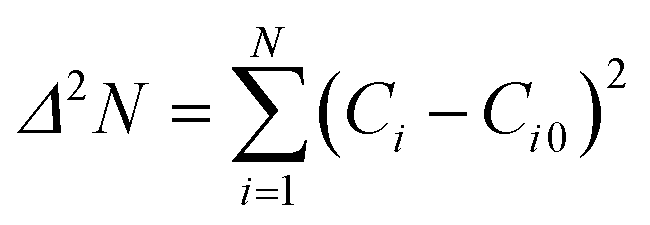 | (4) |
Ci0 is the texture coefficient (=1) in the overhead relation. Δ indicates the degree of preferred orientation of a sample; a zero (≃0) value of the degree of preferred orientation (Δ) acclaims that the material has utterly random orientation; a higher degree of preferred orientation (Δ) leads to amended preferential orientation. The value of the degree of preferred orientation (Δ) was found to be 9.6751 × 10⁻⁴ for the CdIn2Se4 ternary semiconducting compound.46
The Bravais theory determines the distance between the crystal planes, i.e., d-interplanar spacing (dhkl), to shed light on the synthesized material's growth. Based on his tactic, Bravais offers the relation  , where Rhkl is the growth rate of the plane. For a given set of cell parameters for the CdIn2Se4 crystal system (a, b, c, α, β, γ), the d-interplanar spacing (dhkl) for four significant peaks [(111), (201), (202), and (113)] can be intended by using eqn (5):47
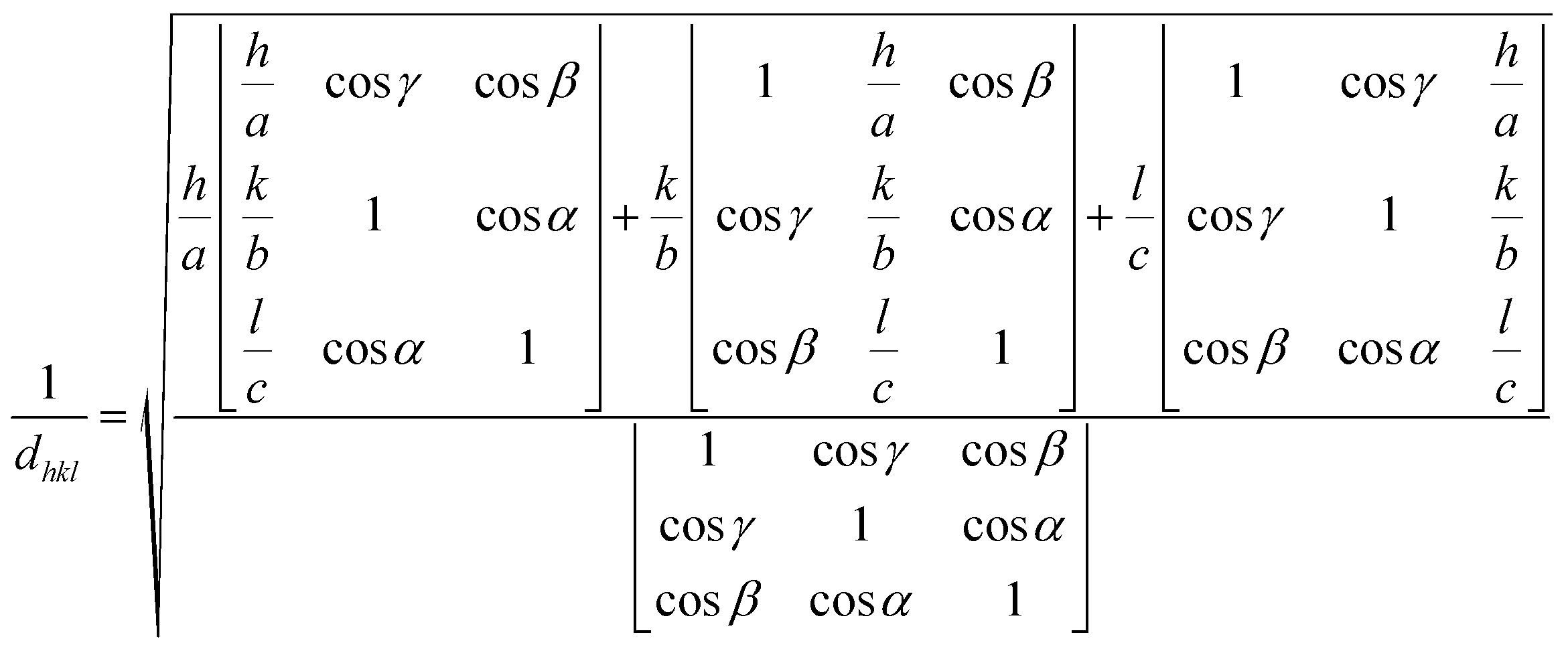 | (5) |
As evident from Table 2, the calculated d-interplanar spacing (dhkl) for four significant peaks of CdIn2Se4 confirms that d111 is the largest, inferring that h111 is the smallest, i.e., the growth rate of the (111) plane R111 is the smallest according to Bravais theory.47 The Bravais theory confirms the growth of CdIn2Se4's (111) plane.48
Using the Miller indices for the prime (111) plane, the tetragonal crystal system's eqn (6) used to obtain the lattice constant (a) of the α-CdIn2Se4 ternary semiconducting compound,44
| d−2 = a−2(h2 + k2) + c−2l2 | (6) |
The lattice parameter's (a) figured moral (in ascending order) is comparable to the datasets (Table 3). The tetragonal crystal system's relation V = a2c (≃a3 for α-CdIn2Se4 ternary semiconducting compound) makes it possible to infer the unit cell volume (V) of the ternary semiconducting compound CdIn2Se4.49
Comparing ternary semiconducting compound CdIn2Se4's unit cell parameter (a) to standard data reveals a 0.052% anomaly.
3.2. Rietveld refinement (RR)
The Rietveld refinement (RR) method in the FullProf suite was used to evaluate the X-ray diffraction (XRD) data to estimate CdIn2Se4's thermal and structural parameters [J thoroughly. Rodriguez-Caravajal, Fullprof Version, 7.40]. The X-ray diffractogram of the ternary semiconducting compound CdIn2Se4 system following Rietveld refinement (RR) is shown in Fig. 2. | ||
| Fig. 2 Rietveld profile fitting of the ternary semiconducting compound CdIn2Se4. | ||
Rietveld refined data points and added structural factors were selected to define the backdrop during refining. The red solid circles epitomize the ternary semiconducting compound CdIn2Se4's observed (experimental) diffractogram, and the black solid circles signify the pattern retrieved from Rietveld refinement (RR), the vertical bars designate the Bragg's position, and the bottommost line stipulates the difference between the observed and calculated profiles. The structural analysis defined peak shapes and full width at half maxima (FWHM) using a linear alliance of a Gaussian and a Lorentzian function (pseudo-Voigt) at various Bragg positions.
Fig. 3 denotes the polyhedron depiction of the ternary semiconducting compound CdIn2Se4's unit cell with a tetragonal structure formed by the VESTA program.4 The ternary semiconducting compound CdIn2Se4 bulk system does not designate any impurity phase/s. It is apparent from the polyhedra unit cell that the CdSe4 tetrahedra share corners with the eight corresponding InSe4 tetrahedra that are formed by bonding Cd2+ to four equivalent Se2− atoms. When In3+ is linked to four comparable Se2− atoms, InSe4 tetrahedra are created, which share corners with four CdSe4 tetrahedra and corners with four InSe4 tetrahedra. In a trigonal non-coplanar geometry, Se2− is joined to one Cd2+ and two equivalent In3+ atoms.
 | ||
| Fig. 3 Polyhedron representation of the tetragonal structure of the ternary semiconducting compound CdIn2Se4. | ||
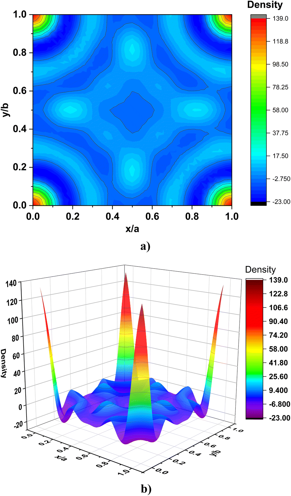
Fig. 4a and b exemplify the electron density inside the ternary semiconducting compound CdIn2Se4 unit cell using the GFourier tool in the FullProf Package. The electron density was measured in electrons per cubic angstrom (e Å−3). Bond distances and angles for the ternary semiconducting compound CdIn2Se4 system were calculated using the VESTA tool with the X-ray diffraction (XRD) parameters obtained after structural refinement with FullProf, which was then used to produce a crystallographic information file (CIF).54 Cd2+ cations lodge the Wycoff (1a) sites at (0, 0, 0), In3+ cations lodge at the Wycoff site 2f at two different positions  and
and  , respectively, whereas Se2− anions lodge the Wycoff (4n) sites at four different positions (0.7279, 0.2720, 0.7636), (0.2720, 0.2720, 0.2363), (0.2720, 0.7279, 0.7636), and (0.7279, 0.7279, 0.2363) in the ternary semiconducting compound CdIn2Se4 system [ICDD card 01-089-2388].30 The cell parameters (a, b, c, α, β, γ) and their error bars are resolute using a tetragonal structure with the P2m(111) symmetry for the ternary semiconducting compound CdIn2Se4. Numerous reliability parameters such as Bragg's R-factor (RB%), profile factor (Rp%), crystallographic factor (RF%), weighted profile factor (Rwp%), expected profile factor (Rexp%), goodness of fit (S), chi2 (χ2%), crystal cell volume (V), and profile parameters (u, v, and w) for the ternary semiconducting compound CdIn2Se4 system are construed and presented in Table 4. The values in bracket designate error bars.
 | ||
| Fig. 4 (a) 2D, and (b) 3D electron density maps of individual atoms on the x–y (z = 0) plane in the unit cell of the ternary semiconducting compound CdIn2Se4. | ||
| Parameters | Symbol/unit | Values |
|---|---|---|
| Cell parameters | a = b (Å) | 5.81385 (0) |
| c (Å) | 5.81536 (0) | |
| α = β = γ | 90.00° | |
| Space group | SG | P2m(111) |
| Bragg's R-factor | RB% | 25.0 |
| Profile factor | Rp% | 24.9 |
| Crystallographic factor | RF% | 22.2 |
| Weighted profile factor | Rwp% | 17.2 |
| Expected profile factor | Rexp% | 13.5 |
| Goodness of fit | S | 1.27 |
| Chi2 | χ2% | 0.12 |
| Crystal cell volume | V (Å3) | 196.564 (0.000) |
| Profile parameters | u | 0.060332 |
| v | −0.026456 | |
| w | 0.037855 |
Electron density mapping is used to study the spreading of electron densities within the tetragonal cell to extricate between the atomic positions of the elements in a crystal's unit cell. The scattering electron density is approached using eqn (7) and the Fourier Transform of the geometrical structural factor ρ(x, y, z) (electron density at a point x, y, z inside a unit cell volume V),55
| ρ(x, y, z) × V = ∑|Fhkl| exp{−2πi(hx + ky + lz − αhkl)} | (7) |
The amplitude of the structure component is symbolized by Fhkl, while the phase angle of each Bragg reflection is symbolized by αhkl. A two (2D)- or three (3D)-dimensional Fourier map was used to exemplify the electron scattering density ρ(x, y, z). Typically, the contours in a two-dimensional (2D) Fourier plot portray the distribution of electron concentrations adjacent to each element in the solution. Elements housed in unit cells tend to be heavier when their electron density contours are thick and dense; a three-dimensional (3D) Fourier map encapsulates a network resembling chicken wire with a single electron density level. Fig. 4a demonstrates the two-dimensional (2D) Fourier electron density mapping of the cadmium (Cd), indium (In), and selenium (Se) atoms in the ternary semiconducting compound CdIn2Se4 unit cell on the x–y plane (z = 0). The electron distribution in the valence 4s and 3d orbitals might cause the contours around the cadmium (Cd). The silhouette in Fig. 4a displays the electron density levels with the coloured area surrounding cadmium (Cd), indium (In), and selenium (Se); on the contrary, the black line expresses the zero-level density contour. The three-dimensional (3D) Fourier density mapping of the cadmium (Cd), indium (In), and selenium (Se) elements in the ternary semiconducting compound CdIn2Se4 unit cell at z = 0 is shown in Fig. 4b.
Table 5 clearly presents the bond (interatomic) lengths, bond angles, and atom parameters (characteristics) of the ternary semiconducting compound CdIn2Se4.29
| Bond length (Å) | Bond angle (degree) | ||
|---|---|---|---|
| Cd1–Se1 | 2.6248 (0) | Se1–Cd1–Se1 | 116.8559 (0) |
| Cd2–Se2 | 2.6254 (0) | Se2–Cd2–Se2 | 105.9128 (0) |
| Cd–Cd | 5.8138 (0) | Cd1–Se1–In1 | 104.6155 (0) |
| In–Se | 2.5708 (0) | Cd2–Se2–In2 | 104.5964 (0) |
| Se1–In1–Se1 | 106.7785 (0) | ||
| Se2–In2–Se2 | 117.9247 (0) | ||
| Se3–In3–Se3 | 104.0534 (0) | ||
| Atomic parameters | |||||
|---|---|---|---|---|---|
| Atom | x | y | z | Occupancy | Multiplicity |
| Cd | 0.00000 (0) | 0.00000 (0) | 0.00000 (0) | 1.046 (0) | 1 |
| In1 | 0.50000 (0) | 0.0000 (0) | 0.50000 (0) | 0.868 (0) | 2 |
| In2 | 0.0000 (0) | 0.50000 (0) | 0.50000 (0) | 1.000 (0) | 2 |
| Se1 | 0.72790 (0) | 0.27200 (0) | 0.76360 (0) | 1.087 (0) | 4 |
| Se2 | 0.27200 (0) | 0.27200 (0) | 0.23630 (0) | 0.994 (0) | 4 |
| Se3 | 0.27200 (0) | 0.72790 (0) | 0.76360 (0) | 1.000 (0) | 4 |
| Se4 | 0.72790 (0) | 0.72790 (0) | 0.23630 (0) | 1.001 (0) | 4 |
3.3. Microstructural parameter analysis
Inspecting the microstructural characteristics of the semiconducting material formerly used to create advanced technological devices is decisive. Several microstructural properties, including lattice parameters (a, b, and c), crystallite size (D), lattice strain (ε), root mean square strain (εrms), dislocation density (δ), lattice stress (σ) and energy density (u) can be inferred by examining the X-ray diffractogram of the ternary semiconducting compound CdIn2Se4.56–58 Following the Gaussian and Lorentzian distribution functions, the peak shape corrects the full width at half maximum (FWHM). As a result of internal lattice stress (σ), lattice strain (ε) causes a unit cell's length to be stretched or compressed relative to its original dimension. Contingent on the crystallite size (D) and lattice strain (ε), Bragg's peak has diverse effects; crystallite size (D) and lattice strain (ε) influence peak width, whereas the intensity of the peak affects the diffraction angle (2θ) position. Diverse approaches were used in the present investigation to examine the ternary semiconducting compound CdIn2Se4's microstructural parameters.
 | (8) |
In the Nelson–Riley (N–R) plot (Fig. 5), the intercept was used to gauge the lattice parameter [Intercept = a (≃c)] of the tetragonal α-phase CdIn2Se4 ternary semiconducting compound, and the outcome is accessible in Table 3.
 | ||
| Fig. 5 N–R diagram of the ternary semiconducting compound CdIn2Se4. | ||
|
Dβcosθ = Kλ
| (9) |
The estimate of the crystallite size (D) is based on the default value of 0.9 for the Scherrer constant (K) since its exact value is unknown for the current material system (CdIn2Se4 ternary semiconducting compound). Re-arranging eqn (9), we obtained eqn (10):
 | (10) |
The crystallite size (D) (=K × λ × slope = 1.3869 × 10⁻¹⁰ × slope) of the CdIn2Se4 ternary semiconducting compound was estimated from the Scherrer plot (Fig. 6a), and is presented in Table 6.
 | ||
| Fig. 6 (a) Sherrer, (b) S–W, (c) εrms–ε, and (d) Monshi plots for the ternary semiconducting compound CdIn2Se4. | ||
| Method | Microstructural parameters | ||||
|---|---|---|---|---|---|
| D (nm) | ε (×10−3) | σ (×106) (Pa) | u (×103) (J m−3) | ||
| Scherrer | 67.9983 | 0.0428 | - | - | |
| Monshi | 70.8019 | — | - | - | |
| W–H | UDM | 66.0429 | −0.1304 | - | - |
| USDM | 69.0000 | — | −2.8496 | - | |
| UDEDM | 68.3202 | — | - | 0.1860 | |
| SSP | 70.7602 | −0.1811 | - | - | |
| H–W | 78.6733 | −1.1750 | - | - | |
The Stokes–Wilson (S–W) eqn (11) was utilized to ascertain the lattice strain (ε) persuaded in the CdIn2Se4 ternary semiconducting compound as a result of crystal imperfection and disorder:59
| β = 4ε tan θ | (11) |
The middling lattice strain (ε) (=0.25 × slope) envisioned from the Stokes–Wilson (S–W) plot (Fig. 6b), for the CdIn2Se4 ternary semiconducting compound is accessible in Table 6.
The CdIn2Se4 ternary semiconducting compound's root mean square strain (εrms) was determined using the Stocks–Wilson (S–W) eqn (12) along each crystallographic plane [(111), (201), (202), and (113)]:59
 | (12) |
The fact that the data points are lying straight with an abscissa at an angle of 38.5864° is clear from Fig. 6c, which shows that the root mean square strain (εrms) varies linearly with lattice strain (ε), demonstrating that the lattice planes' crystallographic direction is consistent.60
 | (13) |
The crystallite size (D) (=K × λ × e−intercept = 1.3869 × 10⁻¹⁰ × e−intercept) for the CdIn2Se4 ternary semiconducting compound was estimated from Fig. 6d, and is presented in Table 6.
 | (14) |
Williamson–Smallman's (W–S) method deduces ≃0.2163 × 10⁻³ lines nm−2 (ref. 56) dislocation density (δ) for the ternary semiconducting compound CdIn2Se4.
3.3.5.1. Uniform deformation model (UDM) method. Due to crystal defects and distortion, the CdIn2Se4 ternary semiconducting compound's crystallite size (D) and lattice strain (ε) can be estimated using the uniform deformation model (UDM) approach, which is derived by modifying the Williamson–Hall (W–H) eqn (15):64
 | (15) |
Table 6 provides the crystallite size (D) (=K × λ × intercept−1 = 1.3869 × 10⁻¹⁰ × intercept−1) and lattice strain (ε) (=slope) obtained using Fig. 7a as a straight-line plot.
 | ||
| Fig. 7 W–H plots: (a) UDM, (b) USDM, and (c) UDEDM for the ternary semiconducting compound CdIn2Se4. | ||
3.3.5.2. Uniform stress deformation model (USDM) method. The Williamson–Hall (W–H) equation needs to be modified to consider the characteristics of an anisotropic crystal because the uniform deformation model (UDM) approach has the flaw of assuming an isotropic, homogeneous crystal, which is not the case in the actual crystallographic system. Hooke's law states that lattice strain (ε) and lattice stress (σ) are linearly related within the elastic limit, resulting in lattice stress (σ) = lattice strain (ε) × Young's modulus (y). By replacing the lattice strain (ε) by
 into eqn (15), we obtained eqn (16):63
 | (16) |
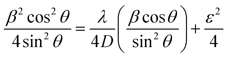
To estimate the crystallite size (D) and lattice stress (σ) of the ternary semiconducting compound CdIn2Se4, eqn (16) requires the values of Young's modulus (y) for each (hkl) plane (yhkl) [(111), (201), (202), and (113)].
For the tetragonal crystal system, eqn (17) relates Young's modulus (y) for each (hkl) plane (yhkl) with elastic compliance constants (Sij) and stiffness constants (Cij):5
 | (17) |
Young's modulus (yhkl) for preferred orientations (111), (201), (202), and (113) were determined to be 29.1266, 28.9776, 28.8912, and 25.0328 GPa, respectively, for the ternary semiconducting compound CdIn2Se4 by entering values of various elastic compliance constants (Sij) into eqn (17).4 By substituting Young's modulus (yhkl) values derived by using eqn (17) into eqn (16) and plotting Fig. 7b, the plot's straight line derives the crystallite size (D) (=K × λ × intercept−1 = 1.3869 × 10⁻¹⁰ × intercept−1) and lattice stress (σ) (=slope) for ternary semiconducting compound CdIn2Se4. The extracted values are presented in Table 6.
3.3.5.3. Uniform deformation energy density model (UDEDM) method. As required by Hooke's law, the uniform stress deformation model (USDM) assumes a linear relationship between the lattice strain (ε) and the lattice stress (σ). However, imperfections such as dislocations and agglomerations make accounting for real crystals' isotropic nature and linear proportionality impossible. In particular, the uniform anisotropic deformation of the lattice in all crystallographic directions and the origin of deformation, which is characterized as the deformation energy density (u)
 ,63 are considered by the uniform deformation energy density model (UDEDM) technique. By substituting
  into eqn (15), we obtained eqn (18):
 | (18) |
Table 6 presents the crystallite size (D) (=K × λ × intercept−1 = 1.3869 × 10⁻¹⁰ × intercept−1) and energy density (u) (=slope2) of the ternary semiconducting compound CdIn2Se4, estimated from the straight-line plot in Fig. 7c.
 | (19) |
 | ||
| Fig. 8 (a) SSP and (b) H–W plots for the ternary semiconducting compound CdIn2Se4. | ||
The plot's linear fitting estimates crystallite size (D) (=K × λ × slope−1 = 1.3869 × 10⁻¹⁰ × slope−1) and lattice strain (ε)  for the ternary semiconducting compound CdIn2Se4. The results are accessible in Table 6.
 | (20) |
The slope shown in Fig. 8b as a straight-line estimates crystallite size (D) (=slope−1), whereas the intercept stretches lattice strain (ε)  of the ternary semiconducting compound CdIn2Se4. The upshots are accessible in Table 6.
Consistency exists between the findings for the various methods' estimated crystallite size (D) and lattice strain (ε) virtues for the ternary semiconducting compound CdIn2Se4. The negative values of lattice strain (ε) and lattice stress (σ) for ternary semiconducting compound CdIn2Se4 indicate compressive lattice strain (ε) and lattice stress (σ) for the ternary semiconducting compound CdIn2Se4, which originates from the assertion of equal and opposing forces that cause a shrinking of the crystalline structure.67,68
3.3.8.1. Bulk modulus (BH). Voigt–Reuss (V–R) methods use eqn (21) and (22) to create a link between the elastic modulus (BV and BR) and elastic stiffness constants (Cij) for tetragonal symmetric crystals:70
| 9BV = 2(C11 + C12) + C33 + 4C13 | (21) |
| BR(C11 + C12 + 2C33 – 4C13) = (C11 + C12)C33 – 2C132 | (22) |
The ternary semiconducting compound CdIn2Se4's bulk modulus (BH) value was found to be 40.7787 Gpa29 by substituting BV (=41.9676 GPa) and BR (=39.5899 GPa) values obtained from eqn (21) and (22) into eqn (23):70
| 2BH = BR + BV | (23) |
The high bulk modulus (BH) of α-phase CdIn2Se4 (40.7787 GPa) in comparison to β-phase CdIn2Se4 (17.6750 GPa) suggests that the compressibility of α-phase CdIn2Se4 is lower, resulting in small volume changes at high pressure, making it appropriate for piezoelectric applications.
3.3.8.2. Shear modulus (GH). In tetragonal symmetric crystals, the Voigt–Reuss (V–R) techniques use eqn (24) and (25) to create a link between the upper and lower bounds for the shear modulus (Gv and GR) and elastic stiffness constants (Cij),70
| 15GV = 2C11 – C12 – 2C13 + C33 + 6C44 + 3C66 | (24) |
 | (25) |
The ternary semiconducting compound CdIn2Se4's shear modulus (GH) value was found to be 15.5735 GPa29 by substituting GV (=17.1652 GPa) and GR (=13.9817 GPa) values obtained from eqn (24) and (25) into eqn (26):70
| 2GH = GR + GV | (26) |
The high shear modulus of α-phase CdIn2Se4 (15.5735 GPa), in comparison to β-phase CdIn2Se4 (14.4220 GPa), indicates that α-CdIn2Se4 has higher retention and resistance to deformation than β-phase CdIn2Se4, which further demonstrates its significant employability in the manufacture of piezoelectric devices.
3.3.8.3. Young's modulus (y) and Poisson's ratio (ν). Young's modulus (y) for the ternary semiconducting compound CdIn2Se4 was found to be 41.4445 GPa29 by substituting the values of bulk modulus (BH) and shear modulus (GH) into eqn (27):70
| y(3BH + GH) = 9BHGH | (27) |
The larger the value of Young's modulus (y), the stiffer the material.69
By placing the values of bulk modulus (BH) and Young's modulus (y) in eqn (28),38 Poisson's ratio (ν) for the ternary semiconducting compound CdIn2Se4 was determined to be 0.3306:29
| 6νBH = 3BH − y | (28) |
Poisson's ratio (ν) usually represents the stability of the material against shear deformation, and its value ranges typically between −1.0 and 0.5 for a stable and linear elastic solid material; a more significant value of Poisson's ratio (ν) indicates that a solid has a good plasticity.
To determine whether a synthesized material is brittle (covalent) or ductile (ionic), the numerical values of Poisson's ratio (ν), Pugh's ratio, the ratio of semiconducting compound's bulk modulus (BH) to shear modulus (GH) (i.e.  ), and Cauchy pressure (=C12 – C44) were utilized. If conditions ν > 0.26,
 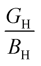 < 0.57, and the positive value of Cauchy pressure is satisfied, a solid is ductile (ionic); otherwise, it is brittle (covalent).38 The ternary semiconducting compound α-CdIn2Se4's ductile (ionic) nature can be confirmed by observing a Poisson ratio (ν) of 0.3306, Pugh's ratio of 2.6185, and a Cauchy pressure of +20.7867 GPa. β-CdIn2Se4 exhibits a brittle (covalent) character in contrast to α-CdIn2Se4.29 As ductile materials have strong damage tolerance qualities, α-phase CdIn2Se4 is a promising contender for piezoelectric applications.
Hardness, an important mechanical property of a material, can be predictable by a Vickers hardness (HV) (theoretical) model using eqn (29):38
 | (29) |
The value of HV was found to be 5.9492 × 10⁵ for the ternary semiconducting compound CdIn2Se4.
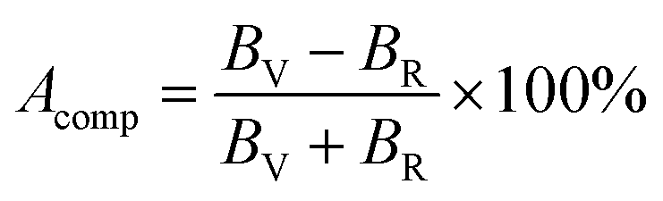
3.3.8.4. Elastic anisotropy. Phase transitions, precipitation, dislocation dynamics, anisotropic plastic deformation, crack behavior, and other mechanical and physical properties of materials all depend on elastic anisotropy. Random crystals are known to have anisotropic elastic properties; consequently, measuring the crystals' elastic anisotropy is necessary since precise anisotropy characterization is essential for practical applications of any material. Eqn (30)–(32) can be used to determine the universal elastic anisotropic index (AU), percent compressible anisotropy (Acomp), and percent shear anisotropy (Ashear), which are used to characterize the elastic anisotropy of solids. For the ternary semiconducting compound CdIn2Se4, the values were found to be 1.1985, 2.9153%, and 10.2211%, respectively,38
 | (30) |
 | (31) |
 | (32) |
Additionally, shear anisotropic factors, A1, A2, and A3, of the tetragonal ternary semiconducting compound CdIn2Se4 were determined using eqn (33)–(35) to be 2.3048, 3.3005, and 2.8479, respectively,69
| A1(C11C33 – C132) = C44(C11 + C33 + 2C13) | (33) |
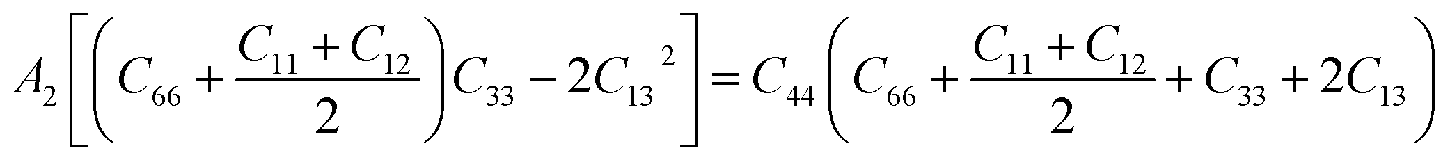 | (34) |
| A3(C11 – C22) = 2C66 | (35) |
The existence of elastic anisotropy in the ternary semiconducting compound CdIn2Se4 is demonstrated by the fact that its elastic anisotropic parameters do not satisfy the following two conditions: (1) AU = Acomp = Ashear = 0 and (2) A1 = A2 = A3 = 1.69
 | (36) |
 , for the ternary semiconducting compound CdIn2Se4 is 3.3296 km s−1.27,28,70 The average wave velocity (vm) for the ternary semiconducting compound CdIn2Se4 was found to be 1.8783 km s−1 obtainable by utilizing the relation
  .70
.70An important characteristic that relates to specific heat and melting point is the Debye temperature (θD), the temperature at whi'h a crystal's maximum vibration mode occurs. The Debye temperature (θD) can be deduced by employing eqn (37):38
 | (37) |
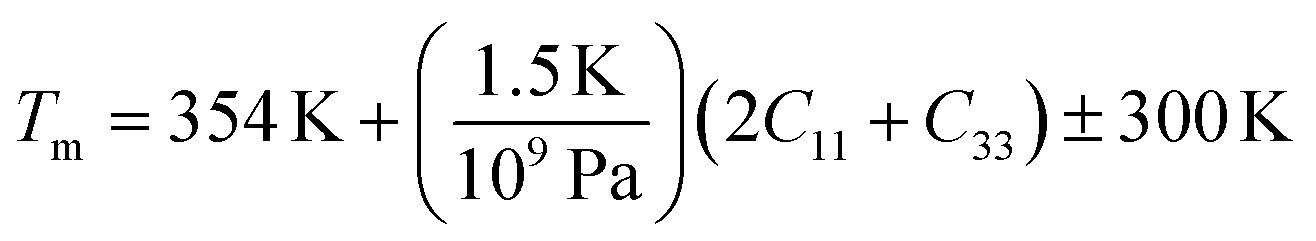
In the above relation, h is the Planck constant (≃6.6262 × 10⁻³⁴ J s), n is the atom number per formula unit of the CdIn2Se4 ternary semiconducting compound (=7), NA' is Avogadro's number (≃6.0224 × 10²³ mol−1), ρ is the density of CdIn2Se4 [refer to Section 4.5 for ternary semiconducting compound CdIn2Se4' density (ρ) value], kB is the Boltzmann constant (≃1.3807 × 10⁻²³ J K−1), M is the molecular weight of ternary semiconducting compound CdIn2Se4 (≃0.6579 kg mol−1), and vm is the average wave velocity. For the ternary semiconducting compound CdIn2Se4, the Debye temperature (θD) was found to be ≃183.9084 K.29 The relatively low value of the Debye temperature (θD) (≃183.9084 K) implies a relatively weak chemical bonding strength in the ternary semiconducting compound CdIn2Se4, which may result in relatively low hardness (5.9492 × 10⁵).69 The mechanical characteristics of the ternary semiconducting compounds α-CdIn2Se4 and β-CdIn2Se4 are compared in Table 7. The authors used β-CdIn2Se4 as the mechanical properties of α-CdIn2Se4 have not yet been published.
| Mechanical properties | α-CdIn2Se4 | β-CdIn2Se4 (ref. 29) |
|---|---|---|
| Bulk modulus (BH) (GPa) | 40.7787 | 17.6750 |
| Shear modulus (GH) (GPa) | 15.5735 | 14.4220 |
| Young's modulus (y) (GPa) | 41.4445 | 33.9660 |
| Poisson's ratio (ν) | 0.3306 | 0.1800 |
| Pugh's ratio | 2.6185 | 1.2300 |
| Cauchy pressure (GPa) | +20.7867 | −09.3980 |
| Elastic anisotropy: universal elastic anisotropic index (AU) | 1.1985 | — |
| Elastic anisotropy: percent compressible anisotropy (Acomp) (%) | 2.9153 | — |
| Elastic anisotropy: percent shear anisotropy (Ashear) (%) | 10.2211 | — |
| Melting temperature (Tm) (K) | 598.4678 ± 300 | 484.4300 ± 300 |
| Transverse sound velocity (vt) (km s−1) | 1.6749 | 0.0002 |
| Longitudinal sound velocity (vl) (km s−1) | 3.3296 | 0.0003 |
| Average wave velocity (vm) (km s−1) | 1.8783 | — |
| Debye temperature (θD) (K) | 183.9084 | 172.9490 |
3.4. Energy-dispersive analysis of X-rays (EDAX)
After grinding the ternary semiconducting compound CdIn2Se4 into a fine powder, it was positioned on a specimen holder for scrutiny by energy-dispersive analysis using an X-ray (EDAX) instrument. First, the ingot was scrutinized by gross analysis, which involved scanning different specimen areas. Next, different points from the specimen were randomly chosen and examined. The ternary semiconducting compound CdIn2Se4's energy-dispersive analysis of X-rays (EDAX), as shown in Fig. 9a and b, makes it evident that the ingot did not exhibit any discernible variation in the stoichiometric constituents of the elements, indicating that the ingot is homogeneous and stoichiometric. The empirical formula CdIn2Se4 has a stoichiometric weight percentage of Cd17.09In34.91Se48.01, whereas the observed weight percentage is Cd16.82In33.78Se49.40. The energy-dispersive analysis of X-ray (EDAX) spectra show a 1.5658 wt% deviation in cadmium (Cd), 3.2124 in indium (In), and 2.8929 in selenium (Se) when equated to their stoichiometric weight percentage.4,48 | ||
| Fig. 9 (a) EDAX spectra of the ternary semiconducting compound CdIn2Se4. (b) Bar graph showing the calculated and observed weight percentages of Cd, In, and Se. | ||
Fig. 10a displays the co-occurrence of all three elements. Fig. 10b–d show separate cadmium (Cd), indium (In), and selenium (Se) distributions, respectively. Cadmium (Cd), indium (In), and selenium (Se) are visualized on an elemental map with three distinct colours, dark blue (hexadecimal colour #000096; RGB values of R: 0, G: 0, B: 150, CMYK values of C: 1, M: 1, Y: 0, K: 0.41), cyan (hexadecimal colour #13CDE8; RGB values of R: 19, G: 205, B: 232, CMYK values of C: 0.92, M: 0.12, Y: 0, K: 0.09), and green (hexadecimal colour #37DC2D; RGB values of R: 55, G: 220, B: 45, CMYK values of C: 0.75, M: 0, Y: 0.80, K: 0.14); each of the three elements' numbers and colours indicate their relative concentrations.
 | ||
| Fig. 10 Elemental mapping of the ternary semiconducting compound CdIn2Se4. | ||
3.5. Density measurement (ρ)
The ternary semiconducting compound CdIn2Se4 was measured for density (ρ) using a densitometer (pycnometer), and the outcomes propose that the lump is undeviating throughout its surface; the study's average density (ρ) value of 5551.2204 kg m−3 favours with the attested value [ICDD card 01-089-2388].29,503.6. Fourier transform infrared (FTIR) spectroscopy
Fig. 11 displays the room-temperature (RT) (≃300 K)-recorded Fourier transform infrared (FTIR) spectra of the ternary semiconducting compound CdIn2Se4. In synthesizing the ternary semiconducting compound CdIn2Se4, only 5 N (99.999%) pure cadmium (Cd), indium (In), and selenium (Se) were employed; no other chemicals or chemical routes were used. A peak perceived at a wavenumber () of 2021.53 cm−1 can be assigned to the stretching N![[double bond, length as m-dash]](https://www.rsc.org/images/entities/char_e001.gif) CS functional group and isothiocyanate class. A peak realized at a wavenumber () of 2157.15 cm−1 can be assigned to the stretching S–C
CS functional group and isothiocyanate class. A peak realized at a wavenumber () of 2157.15 cm−1 can be assigned to the stretching S–C![[triple bond, length as m-dash]](https://www.rsc.org/images/entities/char_e002.gif) N functional group and thiocyanate class and/or stretching NNN functional group and azide class. The absorption peaks due to NCS, S–CN, and/or NNN functional group/s habitually display stout absorption edge in the spectra if existing in the synthesized ternary semiconducting compound CdIn2Se4. The absorption edges are evident from the Fourier transform infrared (FTIR) spectra of the ternary semiconducting compound CdIn2Se4 at 2021.53 cm−1 and 2157.15 cm−1 wavenumbers (), but they are feeble; henceforth, the synthesized ternary semiconducting compound CdIn2Se4 is untainted and free from any functional group.21,73
N functional group and thiocyanate class and/or stretching NNN functional group and azide class. The absorption peaks due to NCS, S–CN, and/or NNN functional group/s habitually display stout absorption edge in the spectra if existing in the synthesized ternary semiconducting compound CdIn2Se4. The absorption edges are evident from the Fourier transform infrared (FTIR) spectra of the ternary semiconducting compound CdIn2Se4 at 2021.53 cm−1 and 2157.15 cm−1 wavenumbers (), but they are feeble; henceforth, the synthesized ternary semiconducting compound CdIn2Se4 is untainted and free from any functional group.21,73
 | ||
| Fig. 11 FTIR spectra of the ternary semiconducting compound CdIn2Se4. | ||
4. Conclusions
CdIn2Se4 belongs to the II–III2–VI4 family. The elastic constants for α-CdIn2Se4 were determined using the CASTEP module in the DFT framework under the PBE-GGA approach. CdIn2Se4 was created by melting 5 N pure stoichiometric amounts of Cd, In, and Se in a microcontroller-based controlled high-temperature rotary furnace. The crystal structure and phase purity of the synthesized CdIn2Se4 compound were investigated by XRD. Significant levels of crystallinity were demonstrated by its modest FWHM of the diffraction peak value and strong XRD peak intensity. The X-ray diffractogram peaks of CdIn2Se4 were recognized, indexed, and perfectly mapped with ICDD card 01-089-2388. The compound has the crystallographic space group (SG) P2m(111) and a single-phase pseudo-cubic α-phase tetragonal (c ≃ a) structure. For the most critical XRD peak (111), the stacking fault (SF) value of CdIn2Se4 was determined to be 1.0267 × 10⁻³. The texture coefficient (Ci) of the XRD peaks of CdIn2Se4 were measured for the preferred orientations of the crystallites along a crystal plane (hkl), and the result was unity. CdIn2Se4 has a degree of preferred orientation (Δ) of 9.6751 × 10⁻⁴. The Bravais theory determines the d-interplanar spacings (dhkl) to shed light on the growth of the synthesized CdIn2Se4 compound, which enables the inference of the significance of the (111) plane of CdIn2Se4. Using Miller indices for the prime (111) plane, the lattice constant (a) of CdIn2Se4 is ≃0.5818 nm, resulting in a cell volume of ≃0.1969 nm3. The Rietveld refinement (RR) in the Fullprof suite was used to evaluate the XRD data to estimate the thermal and structural parameters of CdIn2Se4 with a chi2 value ≃0.12. Several of the CdIn2Se4's microstructural characteristics have been identified. According to the N–R method, the lattice parameter (a) of CdIn2Se4 is ≃0.5817 ± 0.0007 nm. The size of the crystallite (D) was determined by the Scherrer, Monshi, W–H, SSP, and H–W methods to be ≃72.3581 ± 6.3152 nm. The lattice strain (ε) was calculated using the S–W, W–H's UDM, SSP, and H–W methods to be ≃−0.1558 × 10⁻³ ± 25.3500 × 10⁻⁶. In CdIn2Se4, it was found that the root mean square strain (εrms) varies linearly with lattice strain (ε), indicating a consistent crystallographic orientation of the lattice planes. Dislocation density (δ) was calculated using the W–S method (≃0.2163 × 10⁻³ lines nm−2). The lattice stress (σ) was calculated using W–H's USDM approach to be ≃−2.8496 × 10⁶ Pa. W–H's UDEDM-derived energy density (u) is ≃0.1860 × 10³ J m−3. Bulk modulus (BH) (≃40.7787 GPa), shear modulus (GH) (≃15.5735 GPa), Young's modulus (y) (≃41.4445 GPa), Poisson's ratio (ν) (≃0.3306), elastic anisotropy, melting temperature (Tm) (≃598.4678 ± 300 K), transverse sound velocity (vt) (≃1.6749 km s−1), longitudinal sound velocity (vl) (≃3.3296 km s−1), average wave velocity (vm) (≃1.8783 km s−1), and Debye temperature (θD) (≃183.9084 K) were also determined for CdIn2Se4. The stoichiometry and elemental distribution of the synthesized CdIn2Se4 compound were confirmed by EDAX, whereas the density (ρ) (5551.2204 kg m−3) was confirmed using a pycnometer. Through the use of room-temperature (RT) (≃300 K) FTIR spectroscopy in the wavenumber () range of 4000–400 cm−1, the lack of functional groups in the FTIR spectra verified the purity of the synthesized CdIn2Se4 compound.
Data availability
The authors declare that the data supporting the findings of this study are available in the main text of the paper.Author contributions
All authors contributed to the study's conception and design. Material preparation, data collection, and analysis were carried out by S. D. Dhruv, Sergei A. Sharko, Aleksandra I. Serokurova, Nikolai N. Novitskii, D. L. Goroshko, Parth Rayani, Jagruti Jangale, Naveen Agrawal, Vanaraj Solanki, J. H. Markna, Bharat Kataria, and D. K. Dhruv. D. K. Dhruv wrote the first draft of the manuscript, and all authors reviewed and commented on previous versions. All authors read and approved the final manuscript. S. D. Dhruv: data curation, Sergei A. Sharko: conceptualization, Aleksandra I. Serokurova: investigation, Nikolai N. Novitskii: formal analysis, D. L. Goroshko: visualization, Parth Rayani: writing-review & editing, Jagruti Jangale: resources, Naveen Agrawal: validation, Vanaraj Solanki: methodology, J. H. Markna: software, Bharat Kataria: project administration, D. K. Dhruv: writing-original draft, supervision.Conflicts of interest
The submitted work is the authors' original research and has not been submitted elsewhere for publication. On behalf of all co-authors, I declare that there are no conflicts of interest.Acknowledgements
The work was supported by the Department of Science & Technology (DST), Government of India, New Delhi (File number: DST/INT/BLR/P-36/2023), and the Belarusian Republican Foundation for Fundamental Research (File number: F23IND-005) under the India–Belarus Programme of Co-operation in Science & Technology (Joint Research Project). The authors thank the Science and Technology Facilities Council (STFC) for providing access to the CASTEP code for computational work. The authors also express their gratitude to the Sophisticated Instrumentation Centre for Applied Research and Testing (SICART), Vallabh Vidyanagar-388120, Anand, Gujarat, India, for providing access to discounted X-ray diffraction (XRD), energy-dispersive X-ray analysis (EDAX), and Fourier transform infrared (FTIR) spectroscopy facilities.References
- S. I. Radautsan, A. N. Georgobiani and I. M. Tiginyanu, Prog. Cryst. Growth Charact., 1984, 10, 403–412 CrossRef
.
- E. F. M. El-Zaidia, E. A. El-Shazly and H. A. M. Ali, J. Inorg. Organomet. Polym., 2020, 30, 2979–2986 CrossRef CAS
- D. Santamaría-Pérez, O. Gomis, A. L. J. Pereira, R. Vilaplana, C. Popescu, J. A. Sans, F. J. Manjón, P. Rodríguez-Hernández, A. Muñoz, V. V. Ursaki and I. M. Tiginyanu, J. Phys. Chem. C, 2014, 118, 26987–26999 CrossRef
- D. K. Dhruv, B. H. Patel, S. D. Dhruv, P. B. Patel, U. B. Trivedi and N. Agrawal, Mater. Today: Proc., 2023, S2214785323002638 Search PubMed
- S. D. Dhruv, J. Kolte, P. Solanki, V. Solanki, J. H. Markna, B. Kataria, B. A. Amin, N. Agrawal and D. K. Dhruv, Interactions, 2024, 245, 99 CrossRef CAS
- A. N. Georgobiani, B. G. Tagiev, O. B. Tagiev, R. B. Djabbarov, N. N. Musaeva and U. F. Kasumov, Jpn. J. Appl. Phys., 2000, 39, 434 CrossRef CAS
- D. K. Dhruv, B. H. Patel and D. Lakshminarayana, Mater. Res. Innovations, 2016, 20, 285–292 CrossRef CAS
- D. K. Dhruv, B. H. Patel, N. Agrawal, R. Banerjee, S. D. Dhruv, P. B. Patel and V. Patel, J. Mater. Sci.: Mater. Electron., 2022, 33, 24003–24015 CrossRef CAS
- D. K. Dhruv, A. Nowicki, B. H. Patel and V. D. Dhamecha, Surf. Eng., 2015, 31, 556–562 CrossRef CAS
- V. Dhamecha, B. Patel, D. Dhruv and A. Nowicki, Surf. Eng., 2020, 36, 100–105 CrossRef CAS
- M. Tomkiewicz, W. Siripala and R. Tenne, J. Electrochem. Soc., 1984, 131, 736–740 CrossRef CAS
- M. M. El-Nahass, Appl. Phys. A, 1991, 52, 353–357 CrossRef
- H. Neumann, W. Kissinger, F. Lévy, H. Sobotta and V. Riede, Cryst. Res. Technol., 1990, 25, 1455–1459 CrossRef CAS
- H. Neumann, W. Kissinger and F. Lévy, Cryst. Res. Technol., 1990, 25, 1189–1193 CrossRef CAS
- C. Razzetti, T. Besagni, S. Bini and P. P. Lottici, Phys. Status Solidi A, 1989, 111, 411–416 CrossRef CAS
- L. Fornarini, F. Stirpe, E. Cardarelli and B. Scrosati, Solar Cells, 1984, 11, 389–400 CrossRef CAS
- R. Trykozko and D. R. Huffman, J. Appl. Phys., 1981, 52, 5283–5285 CrossRef CAS
- G. Margaritondo, A. D. Katnani and F. Lévy, Phys. Status Solidi B, 1981, 103, 725–731 CrossRef CAS
- J. Przedmojski and B. Pałøz, Phys. Status Solidi A, 1979, 51, K1–K3 CrossRef CAS
- K. Adpakpang, T. Sarakonsri, S. Isoda, Y. Shinoda and C. Thanachayanont, J. Alloys Compd., 2010, 500, 259–263 CrossRef CAS
- A.-A. Ruanthon, T. Sarakonsri and C. Thanachayanont, Funct. Mater. Lett., 2009, 02, 199–203 CrossRef CAS
- S.-H. Choe, B.-N. Park, K.-S. Yu, S.-J. Oh, H.-L. Park and W.-T. Kim, J. Phys. Chem. Solids, 1995, 56, 89–92 CrossRef CAS
- T. G. Kerimova, F. R. Adzalova, R. Kh. Nani and V. Ya. Shteinshreiber, Phys. Status Solidi A, 1981, 67, K143–K146 CrossRef CAS
- E. Guerrero, M. Quintero and J. C. Woolley, J. Phys.: Condens. Matter, 1990, 2, 6119–6126 CrossRef CAS
- E. Fortin and F. Raga, Solid State Commun., 1974, 14, 847–850 CrossRef CAS
- R. Nitsche, J. Phys. Chem. Solids, 1960, 17, 163–165 CrossRef CAS
- I. A. Mamedova, Z. A. Jahangirli, T. G. Kerimova and N. A. Abdullayev, Phys. Status Solidi B, 2023, 260, 2200441 CrossRef CAS
- S. Chandra, A. Sinha and V. Kumar, Int. J. Mod. Phys. B, 2019, 33, 1950340 CrossRef CAS
- A. Priyambada, A. Mohanty and P. Parida, Mater. Today Commun., 2023, 37, 107338 CrossRef CAS
- D. M. Hoat, M. Naseri, R. Ponce-Pérez, J. F. Rivas-Silva and G. H. Cocoletzi, J. Solid State Chem., 2020, 282, 121078 CrossRef CAS
- V. M. Nikale, S. S. Shinde, A. R. Babar, C. H. Bhosale and K. Y. Rajpure, Sol. Energy, 2011, 85, 1336–1342 CrossRef CAS
- V. M. Nikale, S. S. Shinde, A. R. Babar, C. H. Bhosale and K. Y. Rajpure, Sol. Energy, 2011, 85, 325–333 CrossRef CAS
- V. M. Nikale, S. S. Shinde, A. R. Babar, C. H. Bhosale and K. Y. Rajpure, Appl. Sol. Energy, 2010, 46, 194–201 CrossRef
- R. Tenne, Y. Mirovsky, G. Sawatzky and W. Giriat, J. Electrochem. Soc., 1985, 132, 1829–1835 CrossRef CAS
- R. Tenne, Y. Mirovsky, Y. Greenstein and D. Cahen, J. Electrochem. Soc., 1982, 129, 1506–1512 CrossRef CAS
- V. Nikale, Sol. Energy Mater. Sol. Cells, 2004, 82, 3–10 CrossRef CAS
- S. J. Clark, M. D. Segall, C. J. Pickard, P. J. Hasnip, M. I. J. Probert, K. Refson and M. C. Payne, Z. Kristallogr. Cryst. Mater., 2005, 220, 567–570 CrossRef CAS
- W. Bao, D. Liu, P. Li and Y. Duan, Ceram. Int., 2019, 45, 1857–1867 CrossRef CAS
- K. Wark, Thermodynamics, McGraw-Hill, New York, 5th edn, 1988 Search PubMed
- T. Takizawa, C. Komatsu-Hidaka, K. Asaka, T. Isomoto and H. Matsushita, Jpn. J. Appl. Phys., 2000, 39, 35 CrossRef CAS
- B. D. Cullity and S. R. Stock, Elements of X-ray Diffraction, Prentice Hall, Upper Saddle River, NJ, 3rd edn, 2001 Search PubMed
- H. Hahn, G. Frank, W. Klingler, A. D. Störger and G. Störger, Z. Anorg. Allgem. Chem., 1955, 279, 241–270 CrossRef CAS
- R. Suresh, V. Ponnuswamy and R. Mariappan, Appl. Surf. Sci., 2013, 273, 457–464 CrossRef CAS
- S. D. Dhruv, J. Kolte, P. Solanki, M. P. Deshpande, V. Solanki, J. Tailor, N. Agrawal, V. A. Patel, J. H. Markna, B. Kataria and D. K. Dhruv, RSC Adv., 2024, 14, 15455–15467 RSC
- V. M. Nikale, S. S. Shinde, C. H. Bhosale and K. Y. Rajpure, J. Alloys Compd., 2011, 509, 3116–3121 CrossRef CAS
- S. D. Dhruv, J. Kolte, P. Solanki, S. A. Sharko, V. Solanki, J. Tailor, K. Chaudhari, N. Agrawal, V. A. Patel, J. H. Markna, B. Kataria and D. K. Dhruv, J. Mater. Sci.: Mater. Electron., 2024, 35, 1202 CrossRef CAS
- M. Zhang, Y. Chen, C. Qiu, X. Fan, C. Chen and Z. Wang, Phys. E, 2014, 64, 218–223 CrossRef CAS
- B. G. Wagh, A. B. Bhalerao, R. N. Bulakhe and C. D. Lokhande, Mod. Phys. Lett. B, 2015, 29, 1540024 CrossRef
- M. A. M. Seyam, G. F. Salem and S. N. A. Aziz, J. Sol., 2011, 34, 88–98 Search PubMed
- O. Madelung, Semiconductors: Data Handbook, Springer Berlin Heidelberg, Berlin, Heidelberg, 2004 Search PubMed
- J.-H. Ahn, G. Cai, R. S. Mane, V. V. Todkar, A. V. Shaikh, H. Chung, M.-Y. Yoon and S.-H. Han, Appl. Surf. Sci., 2007, 253, 8588–8591 CrossRef CAS
- A. B. Bhalerao, B. G. Wagh, R. N. Bulakhe, P. R. Deshmukh, J.-J. Shim and C. D. Lokhande, J. Photochem. Photobiol. A Chem., 2017, 336, 69–76 CrossRef CAS
- V. M. Nikale, U. B. Suryavanshi and C. H. Bhosale, Mater. Sci. Eng., B, 2006, 134, 94–98 CrossRef CAS
- K. Momma and F. Izumi, J. Appl. Crystallogr., 2011, 44, 1272–1276 CrossRef CAS
- O. Singh, A. Agarwal, S. Sanghi and J. Singh, Int. J. Appl. Ceram. Technol., 2019, 16, 119–129 CrossRef CAS
- A. El-Habib, M. Addou, A. Aouni, M. Diani, J. Zimou and H. Bakkali, Materialia, 2021, 18, 101143 CrossRef CAS
- Y. Canchanya-Huaman, A. F. Mayta-Armas, J. Pomalaya-Velasco, Y. Bendezú-Roca, J. A. Guerra and J. A. Ramos-Guivar, Nanomaterials, 2021, 11, 2311 CrossRef CAS PubMed
- C. M. Magdalane, K. Kaviyarasu, J. J. Vijaya, B. Siddhardha and B. Jeyaraj, J. Photochem. Photobiol. B, 2016, 163, 77–86 CrossRef CAS
- B. Parveen, M. Hassan, Z. Khalid, S. Riaz and S. Naseem, J. Appl. Res. Eng. Technol., 2017, 15, 132–139 CrossRef
- P. Shunmuga Sundaram, T. Sangeetha, S. Rajakarthihan, R. Vijayalaksmi, A. Elangovan and G. Arivazhagan, Phys. B, 2020, 595, 412342 CrossRef CAS
- M. Rabiei, A. Palevicius, A. Monshi, S. Nasiri, A. Vilkauskas and G. Janusas, Nanomaterials, 2020, 10, 1627 CrossRef CAS
- A. Monshi, M. R. Foroughi and M. R. Monshi, World J. Nano Sci. Eng., 2012, 02, 154–160 CrossRef
- D. Nath, F. Singh and R. Das, Mater. Chem. Phys., 2020, 239, 122021 CrossRef CAS
- B. Himabindu, N. S. M. P. Latha Devi and B. Rajini Kanth, Mater. Today: Proc., 2021, 47, 4891–4896 CAS
- K. B. Vinjamuri, S. Viswanadha, H. Basireddy and R. K. Borra, Appl. Mech. Mater., 2021, 903, 27–32 Search PubMed
- M. Basak, Md. L. Rahman, Md. F. Ahmed, B. Biswas and N. Sharmin, J. Alloys Compd., 2022, 895, 162694 CrossRef CAS
- M. P. Deshpande, N. Garg, S. V. Bhatt, B. Soni and S. H. Chaki, Adv. Mater. Res., 2013, 665, 267–282 Search PubMed
- S. Singh, M. C. Rath, A. K. Singh, T. Mukherjee, O. D. Jayakumar, A. K. Tyagi and S. K. Sarkar, Radiat. Phys. Chem., 2011, 80, 736–741 CrossRef CAS
- Y. Wen, X. Zeng, Z. Hu, R. Peng, J. Sun and L. Song, Intermetallics, 2018, 101, 72–80 CrossRef CAS
- J. W. Yang and H. J. Hou, High Pressure Res., 2012, 32, 376–384 CrossRef CAS
- P. Govindaraj, M. Sivasamy, K. Murugan, K. Venugopal and P. Veluswamy, RSC Adv., 2022, 12, 12573–12582 RSC
- K. B. Panda and K. S. Ravi Chandran, Comput. Mater. Sci., 2006, 35, 134–150 CrossRef CAS
- Z. H. Mahmoud, Y. Ajaj, A. M. Hussein, H. N. K. Al-Salman, M. A. Mustafa, E. H. Kadhum, S. Abdullaev, S. A. Khuder, G. K. Ghadir, S. M. Hameed, K. Muzammil, S. Islam and E. Kianfar, Int. J. Biol. Macromol., 2024, 267, 131465 CrossRef CAS
| This journal is © The Royal Society of Chemistry 2025 |