DOI:
10.1039/D5RA00917K
(Paper)
RSC Adv., 2025,
15, 14518-14531
Enhanced photoresponse in a Ag2S/In2Se3 heterojunction based visible light photodetector†
Received
7th February 2025
, Accepted 30th April 2025
First published on 6th May 2025
Abstract
Ag2S and In2Se3, two prominent functional materials, have recently gained extensive research attention. Ag2S shows good chemical stability with excellent photoconducting ability as a direct, narrow band-gap semiconductor. In2Se3 compounds have been widely used in optoelectronics, photodetectors, and gas sensors. In this work, we develop a visible light photodetector by combining these two materials from Ag2S/In2Se3 heterostructure films at room temperature. The Ag2S/In2Se3 bilayer films were annealed at different temperatures, and their photodetection parameters were compared to different annealed films. The bilayer structure and the interdiffusion of Ag2S into the In2Se3 layer were confirmed through a cross-sectional FESEM view. The 250 °C annealed sample shows better photoconductivity with a maximum responsivity of 2.01 × 10⁻¹ A/W and 7.32 × 10⁹ Jones of detectivity than the other films. The current increase from nA to mA upon annealing significantly increased the photo response of the 250 °C annealed films. The hydrophilic properties improved with annealing, as confirmed by contact angle measurement. It is also further verified by the increased porosity observed from the FESEM images of the surface morphology. The transition from amorphous to polycrystalline was confirmed through XRD. The interdiffusion by annealing resulted in the formation of ternary phases like AgInS2 and AgInSe2, as seen from the XRD and HRTEM data. The crystallite size that increased upon annealing reduced the dislocation density from 3.29 × 10¹⁵ to 2.73 × 10¹⁵ m−2. The optical bandgap, density, extinction coefficient, and skin depth showed changes as probed by UV-visible spectroscopy. Upon annealing, the band gap was enhanced by 0.157 eV from its as-prepared state. The observed changes in optical parameters and photoconductivity make the film a suitable candidate for visible light photodetection.
1 Introduction
Bilayer and multilayer film structures are widely used for scheming many optoelectronic devices, including photodetectors, computer disks, optical reflectors, and solar cells.1–4 The charge collection properties are enhanced through a SnSe/SnS hybrid bilayer absorber. The thin SnSe layer improves the fill factor and open-circuit voltage. The efficiency of the bilayer absorber is 3.65%, whereas for single SnS and SnSe layers, the efficiency is 2.87% and 1.4%.5 The mirrors developed from the multilayer As40Se60/Ge25Sb5S70 films are good enough for a microcavity structure for the 1.5 μm telecommunication wavelength.6 The Bi2S3/SnS heterostructure photodetector is very useful for making high-performance optoelectronic devices.7 Such bilayer and multilayer structures have profound technological significance due to the intermixing among the layers. The properties of such materials are enhanced for diffusion between layers by applying various post-energy treatments. The various energy treatments like ion irradiation, laser irradiation, gamma ray irradiation, X-ray irradiation, electron beam irradiation, proton irradiation, thermal annealing, etc. are suitable for such layer's intermixing.8–14
In this aspect, bilayer films of chalcogenides are beneficial in creating innovative nanocomposites with better transport and optical ability. The solid solution formed from the laser-induced interdiffusion of Te into As2Se3 of the Te/As2Se3 bilayer film resulted in an increase in optical absorption with a in bandgap.15 The thermally induced diffusing of Ag layer into Ge20Se50S30 film in the bilayer Ag/Ge20Se50S30 structure resulted in the modification of optical behaviour. The optical energy gap is increased by 0.15 eV due to Ag diffusion, decreasing the disorder.16 The Ag/As30S70 heterostructure in the form of multilayer and bilayer is helpful in phase gratings upon Ar+ ion laser irradiation. The diffraction efficiency of gratings from bilayer film is more than that of multilayers.17 Upon laser exposure, the nanolayered Se/As2S3 reveals the bond switching from As–S to As–Se by Se diffusion, which results in photodarkening phenomena.18 The new AgInSe2 and Ag2Se impurity phases formed from selenized Ag/In/Ag/In multilayers upon heat treatment. The formed compound exhibits n-type conduction, reducing its resistivity with annealing temperature.19 The structural, electrical, and optical entities of the In/Te structure was modified because of the interfacial indium diffusion into the Te layer upon annealing. It resulted in an enhanced hydrophobicity and photocurrent enhancement from nA to ∼mA. These changes are useful for such films in photodetectors, solar cells, and photonic devices.20 In this prospect, our study is based on the bilayer film (Ag2S/In2Se3) with two important chalcogenide compounds such as In2Se3 and Ag2S, for their important application point of view.
In2Se3 belongs to A2IIIB3VI of the periodic table with semiconducting behavior. The chalcogenide compound crystallizes as double-layer Se–In–Se–In–Se stacking along c-axis through Se.21 Such compound is widely used in important applications like phase-change memories, solar cells, and photodiodes. This III–VI binary compound semiconductor has a direct bandgap, which means it can directly emit photons. So, they are well suited for optoelectronics applications, which are important for photovoltaic devices that directly harvest energy from sunlight.22 The α-phase is the most common and has extraordinary piezoelectric and ferroelectric properties. It is a good photodetector as it responds spectrum of light varying from ultraviolet to near-infrared. The 2D In2Se3 is used the applications for intelligent sensing, phase change memory, and in-memory computing devices. It is possible due to the simultaneous coupling of photoelectric, semiconducting, ferroelectric, and phase transition properties.23
In the other hand, silver sulfide (Ag2S) is from I–VI group and behaves as a semiconductor with monoclinic crystal structure. It is a direct tuneable bandgap (Eg = 0.9–1.1 eV) PV material because of the brilliant electrical and optical properties. It possesses low toxicity, good thermal stability, high theoretical efficiency (∼30%), low fabrication cost, and abundant elemental availability.24 Because of its excellent functional properties, Ag2S in its thin film form is used in solar selective coatings, photovoltaic cells, laser recording media, and photoconductor.25 The optical, electronic structure, and electrical properties of nanostructured Ag2S is determined through its microstructure. It includes the composition, size, and shape of the particles.26 Ag2S acts as a good photodetector because of its unique infrared (IR) absorption and emission capabilities.27
In previous studies, the thermal annealing-induced diffusion of dopants into the bottom In2Se3 layer has been reported, and their potential applications have been reported. The transformation from the amorphous to crystalline phase in Ag/In2Se3 by heat energy resulted in the AgIn5Se8 phase formation with increased absorption capability, making it useful for solar cell applications.28 The amorphous to crystalline transition in Bi/In2Se3 upon annealing changes the optical behavior, which is useful for optoelectronics and photovoltaics.29 The temperature-dependent hydrophilicity improvement is noticed by Te diffusion in Te/In2Se3 bilayer heterostructure film for optoelectronic applications.30 Owing to the importance of different dopant diffusion into In2Se3, the current study reports the annealing induced Ag2S layer mixing with the In2Se3 layer in Ag2S/In2Se3 heterostructure at different temperatures and their significant changes in the optical, structural, electrical, surface morphology and surface wettability changes.
In this work, the effect of annealing temperature (100, 150, 200, and 250 °C) on Ag2S/In2Se3 thin films was probed by X-ray diffraction (XRD) and UV-visible spectrophotometry for its structural and optical study. Surface wettability and surface morphology were studied using contact angle and field emission scanning electron microscopy (FESEM). The bilayer heterostructure was verified from the cross-sectional FESEM image. The photodetection study was carried out by the 2450 Keithley source meter at different bias voltages.
2. Experimental methods
2.1. Sample preparation
The heterostructure Ag2S/In2Se3 film with 200 nm as the top Ag2S layer and 600 nm of In2Se3 layer was deposited from Ag2S and In2Se3 ingots (99.999% pure) purchased from Sigma Aldrich. First, the bottom In2Se3 layer was deposited over the cleaned glass substrate inside the Smart Coat 3 HHV coating unit. The chamber pressure was 10−6 Torr, and the deposition rate was 5 Å s−1. The slow rotation of the sample substrate holder through a motor makes the film uniform and homogeneous. The chamber was kept at room temperature by water circulation through a chiller. Next, the top Ag2S layer was coated on In2Se3 layer by maintaining the same experimental conditions. The film thickness during deposition was controlled through the thickness monitor. After that, the films were thermally annealed at four different temperatures for 2 h inside the hot air oven (Scheme 1).
 |
| | Scheme 1 Bilayer film structure and thermal annealing setup. | |
2.2. Experimental characterizations
For structure identification, the prepared samples were characterized through XRD by a D8 Advance X-ray diffractometer. The data were scanned from 10–80° at a scan rate of 0.05° s−1 at a glancing angle of 1°. The X-ray source is CuKα, of 0.1541 nm wavelength. The instrument was operated at a voltage of 40 V with a current of 30 A. The film thickness was verified through a cross-sectional FESEM (JEOL-SEM-7601F) unit. The operating voltage is between 1 and 15 kV with a high vacuum. The images of the film surfaces were captured at different magnifications at various positions. The elemental mapping, along with the composition of the films, was taken by an energy-dispersive X-ray analysis (EDX) unit. The associated planes in the 250 °C annealed film were imaged through selected area electron diffraction (SAED) pattern. The film morphology was again verified from high-resolution transmission electron microscopy (HRTEM, JEM-2100-HRTEM) pictures.
The XPS core level and survey spectra of 250 °C annealed film was recorded from Axis Ultra Kratos Analytical, UK instrument. For this, Al Kα X-rays (1486.6 eV) source was used at a 2 × 10⁻⁹ Torr vacuum. The surface wettability study on all the samples was carried out using a contact angle meter (DMe-211 Plus). The deionized water droplet of 0.5 μL size was used for the data acquisition with 30–35% relative humidity. The data were taken at 3–4 positions to minimize the statistical error. The optical data in the form of transmittance were recorded over 500–2500 nm wavelength range. This was done through a JASCO V-770 UV-visible spectrophotometer with 0.5 nm resolution. Suitable formulas were applied to the primary transmittance data to derive the linear and non-linear parameters.
2.3. Photodetection study
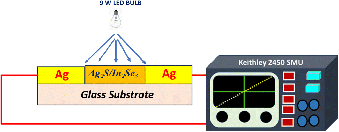
In order to perform a photodetection study, the edges of the bilayer films are scratched from both sides in such a manner that there remains an area of 0.25 cm2 film on a glass substrate. Then, for conductive contact, silver paste was applied on the two opposite sides of the film. These electrodes, known for their simplicity and reliable performance, were used for the measurements. After that, the sample is connected to the Keithley 2450 Source with two probes. As shown in Scheme 2, the prepared film with electrode is mounted on the sample holder. For measurement under light illumination conditions, a 9W white LED bulb was used, as shown in Scheme 2. It covered the entire visible spectrum for illumination. It illuminated the 5 mm × 5 mm sample area for the photo response study. The data was collected many times for reproducibility. Photocurrent data were recorded over −10 V to +10 V voltage with a 0.04 V increment. To ensure electrode uniformity, I–V and I–T data were collected at four separate positions over the film, revealing consistent results. The same procedure was repeated for all samples. The experiment is conducted inside a closed box in a dark room at room temperature to maintain an isothermal environment. To prevent sample heating during illumination, the sample was positioned 10 cm away from the light source. First, the dark current was measured, followed by the current under illumination once the LED light was turned on. These precautions were taken to minimize temperature fluctuations and ensure accurate measurements during the experiment.
 |
| | Scheme 2 Setup for measuring photo response. | |
3. Results and discussions
3.1. Structural investigation: XRD analysis
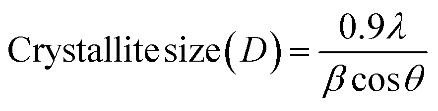
Fig. 1 shows the XRD data of the as-prepared and annealed Ag2S/In2Se3 thin films. The as-prepared sample exhibits an amorphous nature, whereas the heat treatment leads to a polycrystalline behavior. The crystallinity increased with annealing temperature. This increase in the annealing temperature leads to diffusion of phase between the phases of Ag2S and In2Se3. The XRD pattern of the thin films exhibits several peaks, which denote different phases of the films. The peaks appeared around 43.82° and 26.43° corresponding to the AgInSe2 cubic phase (ICDD: 00-023-0636) with (220) and (111) planes. Similarly, the peaks at 25.23° (112), 28.48° (103), and 52.24° (312) were also assigned to the AgInS2 tetragonal phase (ICDD: 01-075-0117). Several structural parameters govern various parameters, such as morphology, particle size, and other optical properties. Hence, these structural parameters can be calculated from Scherrer's relation. The crystallite size (D) denotes to the coherent volume in the thin films for the respective diffraction peak. It also corresponds to the grain size of polycrystalline thin film. It can be written as,31| |
 | (1) |
Here θ denotes Bragg's angle and β represents the full width at half maximum (FWHM). Cu Kα line wavelength is denoted by λ (1.54 Å).
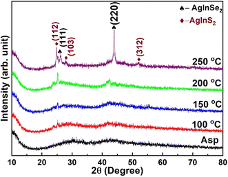 |
| | Fig. 1 Structural data by XRD for Ag2S/In2Se3 films. | |
The distortion created in film dimensions compared to its initial size is represented by lattice strain (ε). The two varieties of such strain are: uniform strains and non-uniform strains. An isotropic contraction/expansion of the unit cell results from regular or consistent strain.32 Peak broadening is unaffected; however, the measured peaks are shifted and the lattice parameters are somewhat altered as a result. Peak broadening is brought on by uneven or nonuniform strain, which also causes atoms to shift irregularly from their initial locations.33 Furthermore, the material's poor crystallization and numerous flaws also contribute to the uneven strain. The relation is used to compute the lattice strain,31
| |
 | (2) |
The density of dislocation, also known as dislocation density (
δ), is defined as the length of dislocation lines per unit volume. From a thermodynamic perspective, dislocations are not as important as observable densities despite being non-equilibrium defects. This is estimated using the relationship,
31| |
 | (3) |
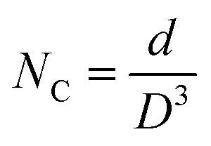
The number of crystallites is always determined by structural factors such as the size of the crystallites and the degree of agglomeration or clustering. The number of crystallite (
NC) is affected by the
D value significantly and evaluated as
| |
 | (4) |
The calculated different structural data are given in Table 1. The D value gradually enhanced with annealing temperature. The high-temperature energy from the recrystallization and re-nucleation process causes the increase in crystallinity. The densification process causes the development of small nuclei that grow on their own and then merge with the more regular ones.34 Many crystallites are created during the annealing process, that increases the absorption surface area. It reduced the optical bandgap by causing more light to be absorbed than transmitted.35
Table 1 Calculated structural data of Ag2S/In2Se3 films
| Structural parameters |
150 °C |
200 °C |
250 °C |
| Average crystallite size (nm) |
17.42 |
18.11 |
19.12 |
| Dislocation density, δ × 1015 (m−2) |
3.29 |
3.04 |
2.73 |
| Lattice strain (ε) |
0.0064 |
0.0066 |
0.0069 |
| NC (nm−2) |
0.15 |
0.13 |
0.11 |
3.2. Morphology study
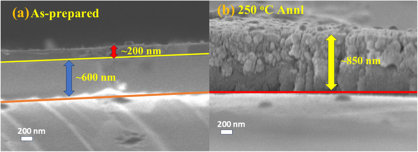
The cross-sectional image of bilayer Ag2S/In2Se3, and 250 °C annealed films is shown in Fig. 2. It perfectly presents the bilayer heterostructure with two distinct layers of Ag2S and In2Se3. The top Ag2S layer shows ∼200 nm thickness, while bottom In2Se3 film is of ∼600 nm, as seen in Fig. 2. However, the 250 °C annealed film is found with an enhanced thickness of ∼850 nm after the intermixing of Ag2S layer into the In2Se3 layer upon heat treatment. The uniformity of Ag2S top layer was not perfect for the smaller thickness value coated within short time. The single layer formed by the intermixing upon annealing for 250 °C is shown in Fig. 2(b).
 |
| | Fig. 2 View of cross-sectional FESEM for bilayer (a) Ag2S/In2Se3, and (b) 250 °C Ag2S/In2Se3 annealed film. | |
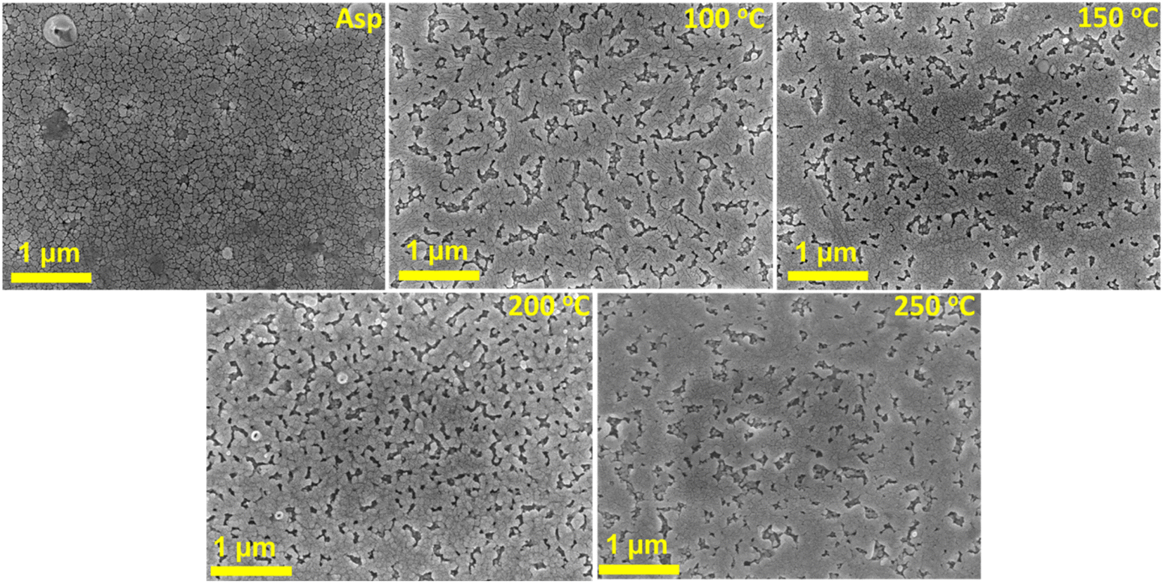
The morphological study acts an important role in deciding the applicability of the material. Fig. 3 represents the FESEM images of the thin films. With the enhancement in the annealing temperature, the particle size increases. Such an increase in the grain boundary also enhanced the porosity of the material. This also affects the absorbance as well as the surface wettability property of the sample. The 100 nm scale FESEM images for all the films are shown in Fig. S1.†
 |
| | Fig. 3 FESEM image of different Ag2Se/In2Se3 films at 1 μm scale. | |
The elemental mapping is shown in Fig. 4. The elemental mapping shows Ag, Se, S, and In presence in the films as verified from the EDX spectra Fig. 4(f). The peak at 2.98 keV belongs to the Ag-atom, while 1.379 keV peak referred as Se-Kα atom. The peaks located at 2.30 and 3.28 keV referred as S and In elements. The extra peaks observed at 0.276 keV and 0.542 keV are attributed to carbon. Carbon tape was used for conducting purposes during data recording. Likewise, the low-intensity 2.133 keV peak corresponds to Au. It was taken as a coating material on the sample surface to minimize charging effects.
 |
| | Fig. 4 (a–e) Elemental mapping and (f) EDX spectra of 250 °C annealed Ag2S/In2Se3 thin film. | |
3.3. TEM analysis
The TEM images of the sample at two different scales are shown in Fig. 5(a and b). Fig. 5(c) shows the HRTEM pictures of the sample showing the existence of both AglnSe2 and AgInS2 phases. The atomic spacing is 3.35 Å (111) and 2.05 Å (220) for Ag2InSe2. Similarly, the atomic spacing of 3.31 Å (111) corresponds to the AgInS2 phase. Furthermore, the SAED pattern also supports the XRD pattern of the material and confirms the presence of different phases (Fig. 5(d)).
 |
| | Fig. 5 (a and b) TEM picture, (c) HRTEM picture, and (d) SAED pattern of 250 °C annealed Ag2Se/In2Se3 thin film. | |
3.4. XPS analysis
XPS analysis plays a crucial part in evaluating the characteristics of Ag2S/In2Se3 thin films, particularly in identifying their elemental composition. Fig. 6(a) exhibits the survey spectra of 250 °C annealed thin films. Here, there are several peaks appeared in the spectra for In 3d, C 1s, Ag 3d, S 2p, and Se 3d. The exact state of the elemental composition can be visualized in the core-level peak of the thin films. Fig. 6(b) represents the Ag 3d core level spectra, which typically feature two significant peaks corresponding to the spin–orbit splitting at binding energies around 368 eV for Ag 3d5/2 and 374 eV for Ag 3d3/2.36 This shows the metallic character of Ag (0). The S 2p peak exhibits (Fig. 6(c)) a doublet structure with 161 eV (S 2p3/2) and 166 eV (S 2p1/2) peaks.37 The In 3d spectrum shown in Fig. 6(d) exhibits peaks at around 444.5 eV and 451.5 eV, corresponding to the 3d5/2 and 3d3/2 components, respectively.38 The Se 3d peak (Fig. 6(e)) appears near 54.5 eV, marking the spin–orbit coupling characteristics specific to this thin film.39
 |
| | Fig. 6 XPS (a)survey, core level (b) Ag 3d, (c) S 2p, (d) In 3d and (e) Se 3d spectra of 250 °C annealed Ag2Se/In2Se3 thin film. | |
3.5. Optical analysis
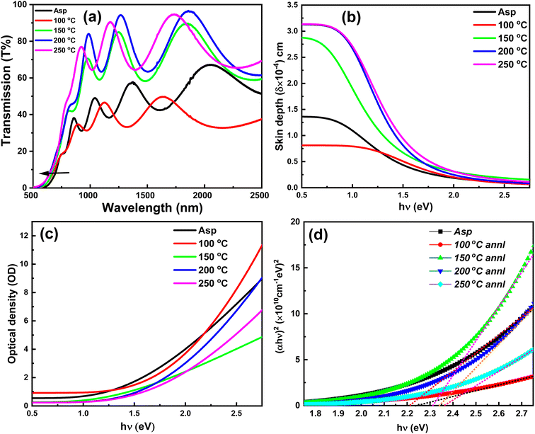
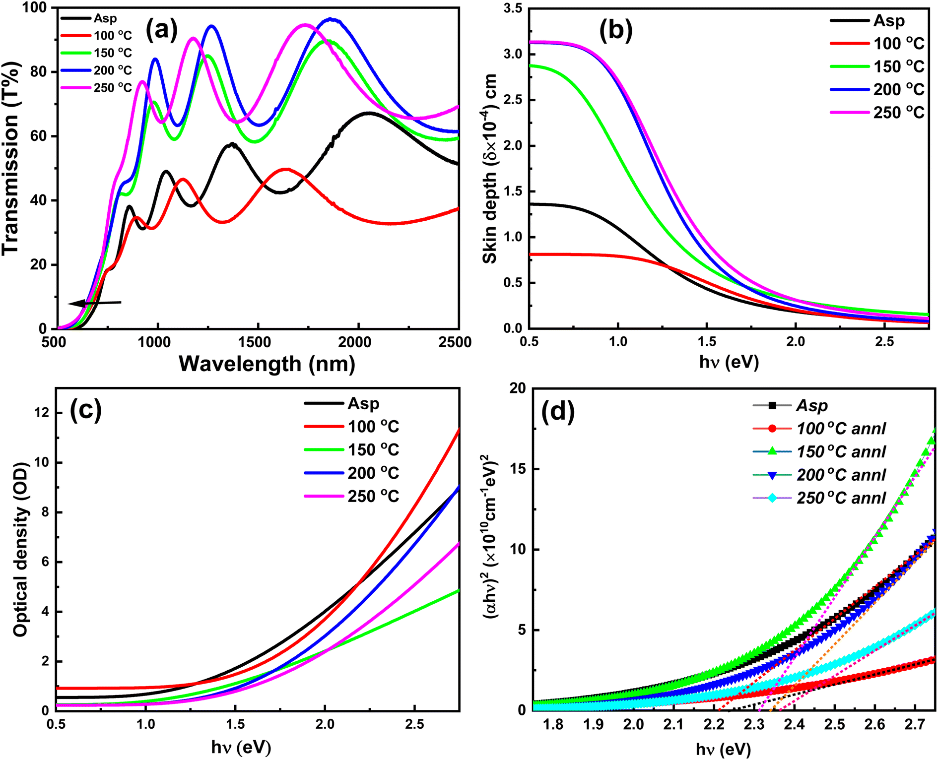
The annealing-induced optical changes are clearly noticed in the transmittance data obtained from the UV-visible spectrometer in Fig. 7(a). The transmission power gradually increased with annealing along with the shift of absorption edge to lower wavelength. This indicates the increase in the energy gap upon annealing. The appearance of fringe patterns in the films infers film homogeneity. The increase of transmittance varies from 40–80% across the wavelength region 800–2000 nm, mostly in near IR regions. The enhanced transmittance with annealing might be for the defect state change in the gap regime and the defect/disorder concentration.40 Since the observed transmittance is less in visible regions (500–800 nm), the absorbance is more, making it suitable for photodetection in visible light regions. It indicates that the films are completely absorbent in the visible regime, making them suitable for optical windows in photovoltaic cells. The higher transparency in the NIR range comes from the free electron interaction with incident energy that led to a change in the polarization of light, making it a more efficient material for IR lenses and waveguides used for temperature monitoring and detection.20,41
 |
| | Fig. 7 (a) Transmittance change (b) skin depth (c) optical density (d) bandgap of the films. | |
The absorbance strength was evaluated from the transmittance spectrum by using the formula  with ‘t’ as the film thickness and ‘T’ as the transmittance value. The calculated absorption coefficient ‘α’ values are used to evaluate the other important optical parameters like skin depth, extinction coefficient, bandgap, optical density, etc. The important metric associated with ‘α’ is the skin depth, the so-called penetration depth (δ). The definition of it lies in the value that equals 1/e times the photon density at the surface level. This parameter is well-linked with the conductivity in semiconducting films and determined by the reciprocal of ‘α’ (δ = 1/α).20 It is observed that the skin depth gradually decreases with an increase in photon energy and saturates at higher energy regions (Fig. 7(b)). The value of δ is smaller for the as-prepared film than the annealed one since high absorbance brings down the transmittance, and light passes through the film with less amount.42 The reverse is for the annealed film with more transmittance and high skin depth. The loss of light while passing through the film by scattering and absorption is represented by the extinction coefficient (k). It is obtained from the wavelength and corresponding absorption coefficient by
  .20 The variation of k at different annealing conditions is presented in Fig. S2.† It infers a lower value for annealed sample over as-prepared bilayer film. Lower ‘k’ values signify the comparatively smoother surface and low loss of light energy by scattering and absorption. Optical density (OD) also measures the absorption strength of the films. It is linked to the film thickness and ‘α’ by OD = α × t. The change in photon energy upon annealing is presented in Fig. 7(c). Its value increases with ‘hν’ and has less magnitude for the annealed sample (Fig. 7(c)).
The vital parameter of the semiconducting films is the energy gap or optical bandgap (Eg), which is dependent on ‘hν’ and the absorption coefficient through the relation,43
The relation has the exponent ‘m’, which has separate values for the type of electronic transitions between gap regions. The different exponent factors for “m” as 2, ½, 3, and 3/2 correspond to indirect allowed, direct allowed, indirect prohibited, and direct prohibited transitions. Fig. S4† presents the direct optical band gap as calculated through the linear fitting between (αhυ)2 with (hυ). The x-intercept presents the bandgap value where the slope gives the Tauc parameter. The films' direct band gap was increased from 2.199 eV (as-prepared Ag2S/In2Se3) to 2.337 eV upon annealing at 250 °C (Fig. 7(d)). This increase in Eg is in accordance with the model developed by Davis and Mott, so-called “density of state model”.44 The enhancement in Eg is because of the decrease in defects with increased structural ordering, as seen from the XRD data. The decreased defect states are represented by the Tauc parameter. The B2 values are 1.81 × 10¹¹, 2.01 × 10¹¹, 2.96 × 10¹¹, 3.94 × 10¹¹, and 4.43 × 1011 cm−2 eV−2 for as-prepared, 100, 150, 200, and 250 °C annealed samples respectively. The inverse relation between the Tauc parameter and disorder strength results in the increased value of B.45 The formation of more saturated bonds with heat treatment reduces the defect states.46 The direct relation with the defect state is presented by another important quantity called Urbach energy (Eu). It is calculated at a very low absorption regime. The Eu was calculated from the relation47  . Here, α0 refers to the corresponding ‘α’ value at the bandgap. By plotting ln
![[thin space (1/6-em)]](https://www.rsc.org/images/entities/char_2009.gif) ‘α’ vs. ‘hν’ (Fig. S3†) and using linear fit, the inverse of slope depicts Eu value. The Eu values are 307, 289, 267, 204, and 198 meV for as-prepared, 100, 150, 200, and 250 °C annealed samples respectively. The decreasing trend of the Eu value infers the reduction of defect states due to structural ordering.48
‘α’ vs. ‘hν’ (Fig. S3†) and using linear fit, the inverse of slope depicts Eu value. The Eu values are 307, 289, 267, 204, and 198 meV for as-prepared, 100, 150, 200, and 250 °C annealed samples respectively. The decreasing trend of the Eu value infers the reduction of defect states due to structural ordering.48
3.6. Surface wettability property study
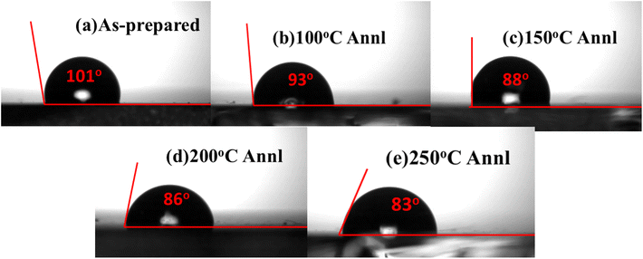
The interaction of the fluid with the sample surface is determined through surface wettability. Such wetting property is common; however, it varies based on chemical nature of both liquid and solid phases. The surface wettability nature of the films is confirmed by their hydrophilicity or hydrophobicity nature as measured through the contact angle between the two phases. The surface with water-loving is called the hydrophilic one with its contact angle (θC) below 90°. On the other hand, the surface with water repelling is called the hydrophobic one with θc greater than 90°.49 The observed contact angle images for different films are presented in Fig. 8. The as-prepared Ag2Se/In2Se3 bilayer film has a θC value of 101°, which indicates its hydrophobic behaviour. However, the contact angle value decreased upon annealing and was found to be 83° for the 250 °C annealed film. This shows the transition of hydrophobicity to hydrophilicity upon annealing. The better photocatalytic performance of the sample depends on the hydrophilic behavior of the surface.50 The FESEM surface images clearly show the increase in porosity that infers the appearance of a hydrophilic nature at the higher annealing temperature.
 |
| | Fig. 8 (a–e) Contact angle pictures of different film samples. | |
The wettability nature is purely associated with sample surface morphology. Appropriate surface modification techniques can modify it. Thermal treatment allows for modifying the hydrophilicity of the surface of a material. Hydrophilic surfaces possess high surface energy that can accelerate the photocatalysis rate over hydrophobic ones.51 The surface energy was evaluated from ‘Young’ equation,  , where γw water surface tension (71.99 Nm m−1).52 The degree of binding strength among film surface and water droplet is expressed by work of adhesion (Wsl). It is calculated by the formula,53 Wsl = γw(1 + cos θC). The value of γse and Wsl are given in Table 2. By dispersing water droplets and forming the film over the hydrophilic surface, it allows light transmittance and reduces pollutants through the photocatalysis process.54
Table 2 Estimated parameters of contact angles of the films
| Parameters/film |
As-prepared |
100 °C annl |
150 °C annl |
200 °C annl |
250 °C annl |
| θC (degree) |
101 |
93 |
88 |
86 |
83 |
| γse (mN m−1) |
11.784 |
16.162 |
19.275 |
20.595 |
22.651 |
| Wsl (mN m−1) |
58.253 |
68.223 |
74.502 |
77.011 |
80.763 |
3.7. Photodetection study
The logarithmic I–V plots under light and dark conditions for each film are shown in Fig. 9 (a–g). The linear I–V variation is presented in Fig. S5† indicating the ohmic nature. The plots reveal distinct, symmetric curves for each thin film under both lighting conditions, with the photocurrent consistently exceeding the dark current in each film. Such photocurrent increment is attributed to light–material interactions and charge separation.55 The maximum photocurrent i.e. light (IL) and dark (ID) current for each film as obtained from Fig. S5† is presented in Table 3. The calculated photosensitivity of each film by using eqn (6) is shown in Table 3. It has been observed that all the films exhibit notable photosensitivity; however, 250 °C annealed Ag2S/In2Se3 thin film sample demonstrates superior photodetection performance over other samples. Increasing the annealing temperature of Ag2S/In2Se3 thin films improved the photodetector performance, including higher photoresponsivity and detectivity due to improved crystallinity.56 The performance of a photodetector under low- and high-light state is primarily explained by the generation of electron–hole pairs proportional to power density. Depositing an Ag2S layer on In2Se3 enhances the carrier concentration in the In2Se3 layer. Additionally, performance is influenced by oxygen adsorption (in the dark) and desorption (under illumination) at the film's surface. In the darkness, adsorbed oxygen ions (O−) capture free electrons (O2 + e− → O2−). Upon illumination, electron–hole pairs are generated, and holes facilitate oxygen desorption, releasing additional free electrons into the conduction band, thereby increasing the photocurrent.57
 |
| | Fig. 9 I–V characteristics plots of as-prepared and annealed Ag2S/In2Se3 thin films plotted in logarithmic scale for both dark and light conditions (a) asp, (b) 100 °C, (c) 150 °C, (d) 200 °C, (e) 250 °C, combined I–V plots of all the samples (f) in dark condition and (g) in light condition. | |
Table 3 The figure of merits of all the Ag2S/In2Se3 thin films
| Sample |
IL (A) |
ID (A) |
IL – ID (A) |
Photo sensitivity (%) |
Responsivity (R) (AW−1) |
Detectivity (D*) (Jones) |
| Asp |
4.62 × 10⁻⁹ |
3.19 × 10⁻⁹ |
1.42 × 10⁻⁹ |
30.88 |
9.25 × 10⁻⁷ |
1.44 × 10⁷ |
| 100 °C |
1.03 × 10⁻⁸ |
3.95 × 10⁻⁹ |
6.35 × 10⁻⁹ |
61.62 |
2.06 × 10⁻⁶ |
2.89 × 10⁷ |
| 150 °C |
2.86 × 10⁻⁷ |
2.66 × 10⁻⁸ |
2.59 × 10⁻⁷ |
90.67 |
5.72 × 10⁻⁵ |
3.09 × 10⁸ |
| 200 °C |
4.04 × 10⁻⁷ |
1.33 × 10⁻⁷ |
2.71 × 10⁻⁷ |
66.98 |
8.09 × 10⁻⁵ |
1.95 × 10⁸ |
| 250 °C |
1.01 × 10⁻³ |
6.07 × 10⁻⁴ |
4.01 × 10⁻⁴ |
39.78 |
2.01 × 10⁻¹ |
7.32 × 10⁹ |
Additional key parameters like, detectivity (D*) and photoresponsivity (R) also determines the photodetector performance. These metrics are determined using specific mathematical relationships and are also tabulated in Table 3.58,59
| |
 | (6) |
| |
 | (7) |
| |
 | (8) |
Here, the value of
A (active surface area) = 0.25 cm
2 and
P (incident light's power density) = 20 m Wcm
−2. The other constant ‘
e’ represents electron charge.
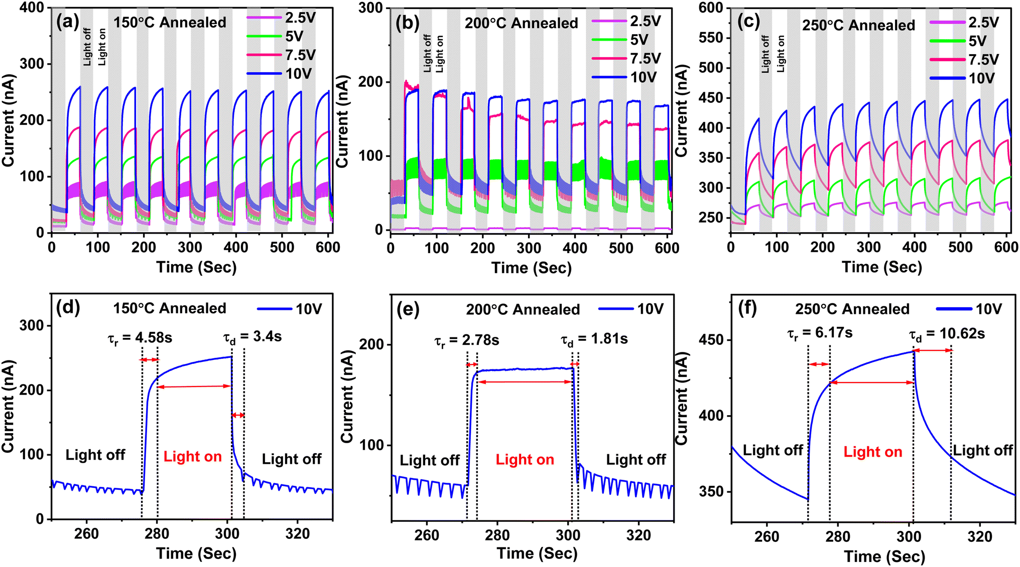
The temporal photo response plot i.e., current versus time (I–T) curves for thin film samples annealed at 150, 200, and 250 °C are presented in Fig. 10(a–c), showing multiple on/off cycles measured with different biasing voltages of 2.5, 5, 7.5, and 10 V. These curves reveal an increase in current under light illumination, which decreases immediately once the light is turned off. The instantaneous rise in current with light exposure is attributed to the increased drift velocity of carriers. Variations in the maximum photocurrent values among the samples are likely due to defect states specific to each material. The results confirm a substantial increase in current under illumination for all three thin films with an increase in biasing voltage, indicating continuous carrier generation during light exposure. The increasing electric field across the photodetector is the main cause of the rise in photocurrent with higher bias voltages. More charge carriers accelerated by this greater electric field can contribute to the current as a result of the more effective separation of photogenerated hole–electron pairs, which reduces recombination by shortening their transit time and raising the carrier drift velocity. Higher bias voltages can further increase the area for efficient charge production and collection by widening the depletion region, which will increase the photocurrent even more.
 |
| | Fig. 10 Temporal photo response curve showing the variation between current and time for different biasing voltages of 2.5, 5, 7.5, and 10 V for different annealed thin films (a) 150 °C, (b) 200 °C, and (c) 250 °C, respectively. Variation in the rise and fall time of photocurrent for different annealed thin films (d) 150 °C, (e) 200 °C, and (f) 250 °C, respectively. | |
When the light is switched off, the photocurrent decreases gradually, likely due to the recombination of injected free carriers with trapped carriers. Additionally, certain temporary variation in photocurrent action is due to change in carrier transport within the devices and for non-radiative pathways. The specific peak between 250 to 330 seconds is selected for all the three films for analysis as illustrated in Fig. 10(d–f). Such peak provides important information towards the performance of each thin film. The associated current values such as (Ion) and (Ioff) for each rise and decay phase of the I–T curves are derived from this peak analysis. These values, along with the Ion/Ioff ratios for the three samples, are compiled in Table 4.
Table 4 Photodetector parameters for Ag2S/In2Se3 thin films at rise and decay conditions
| Sample |
During rise |
During decay |
| Ion (nA) |
Ioff (nA) |
Ion/Ioff |
τr (s) |
Ion (nA) |
Ioff (nA) |
Ion/Ioff |
τd (s) |
| 150 °C |
219.26 |
40.01 |
5.48013 |
4.58 |
262.05 |
59.02 |
4.44002 |
3.4 |
| 200 °C |
172.64 |
59.63 |
2.89519 |
2.78 |
176.33 |
64.79 |
2.72156 |
1.81 |
| 250 °C |
421.51 |
344.94 |
1.22198 |
6.17 |
442.73 |
373.33 |
1.18589 |
10.62 |
The decay time (τd) and rise time (τr) are key parameters in a photodetector's response curve, reflecting how quickly the device reacts to light and comes back to its baseline state after the light is switched off. Here, τr represents the time it need for the photodetector's output to increase from 10 to 90% of its peak current when exposed to light. A shorter τr indicates a faster reaction to the onset of light, showing how swiftly the photodetector transitions from no signal to a detectable output. Conversely, the decay time (τd) refers to the time required for the output current to decrease from 90% to 10% of its peak value after the light source is removed.60 The shorter ‘τd’ indicates that the photodetector can quickly reset or recover, minimizing any residual effects from the previous light stimulus. Both rise time and decay time are crucial for assessing a photodetector's performance. The fast rise time enables the rapid detection of light changes, which is vital for applications needing swift responses to variations in light intensity. Likewise, a short ‘τd’ ensures the detector can promptly recover, allowing it to accurately respond to subsequent changes in light without being affected by prior illumination. The τr and τd values for the photodetector are derived from Fig. 10(d–f) and summarized in Table 4. The I–T stability curve shown in Fig. S6† presents the time-dependent current response of the 250 °C annealed Ag2Se/In2Se3 thin film over a duration of 3600 seconds (∼1 hour). It demonstrates excellent electrical stability over prolonged operation, making it a promising candidate for reliable and durable photodetector applications, especially where consistent long-term performance is crucial.
The performance of the annealed Ag2S/In2Se3 thin films in terms of photodetection is quite good as it shows better responsivity and detectivity. The short rise and fall time of the photocurrent of the thin films testifies to their capability as efficient photodetector devices. Based on the photodetection study of annealed Ag2S/In2Se3 thin films with a maximum responsivity of 2.01 × 10⁻¹ A/W and detectivity of 7.32 × 10⁹ Jones several potential applications such as fabrication of optoelectronic devices, environmental monitoring, communication, imaging, and sensing can be predicted. This study also provides crucial information regarding the effects of enhancing the performance of thin films after increasing the annealing temperature to a certain extent. This study paves the path for the preparation of similar kinds of thin film materials with various optoelectronic applications.
4. Conclusions
The observed changes in the optical, structural, morphology, electrical, and surface wettability in Ag2S/In2Se3 heterostructure film upon annealing at various temperatures demonstrated its applicability in photodetection. The 250 °C annealed film demonstrated good photodetection ability with a maximum responsivity of 2.01 × 10⁻¹ A/W and 7.32 × 10⁹ Jones of detectivity over the other films as well as good stability over a longer period. The photocurrent at both light and dark conditions is in the range of mA over the nA range for other films. The increase in surface energy of the annealed film and the transition of hydrophobicity to hydrophilicity upon annealing makes the annealed film suitable for better photocatalysis applications. The increase in optical bandgap from 2.199 eV from its as-prepared state to 2.337 eV for the 250 °C annealed film signifies the reduction in disorder and increase in crystallinity. The increased crystallite size for the annealed film, as observed from the XRD study, reduces the dislocation density. The development of both AgInSe2 and AgInS2 phases in the annealed film confirms the interdiffusion of the top layer into the bottom layer upon annealing. The cross-sectional FESEM image confirms such diffusion, and the surface morphology of the films changed with more porosity in the film, resulting in more hydrophilic behavior. The TEM study further confirmed the new phases and corresponding planes present in the annealed film. The XPS study verified the chemical states of the corresponding elements. The observed changes in the optical parameters and electrical changes make such films for useful photodetection and optoelectronic applications.
Data availability
All the data related to the present work are included in the manuscript and ESI.†
Conflicts of interest
There are no conflicts to declare.
Acknowledgements
The author, Dr R. Naik, thanks the central instrumentation facility of ICT-IOC for different characterizations and the Science and Engineering Research Board (SERB), Govt. of India.
References
- M. Khan, K. A. Bhatti, R. Qindeel, F. Aleem, N. Rehman and N. Alonizan, Sol-gel deposition and characterization of multilayer 2% Cu doped TiO2 nanostructured thin films, J. Mater. Sci.:Mater. Electron., 2017, 28, 9471–9477 CrossRef CAS.
- M. I. Khan, S. Imran, Shahnawaz, M. Saleem and S. U. Rehman, Annealing effect on the structural, morphological and electrical properties of TiO2/ZnO bilayer thin films, Results Phys., 2018, 8, 249–252 CrossRef.
- J. Kim, K. Barmak, M. D. Graef, L. H. Lewis and D. C. Crew, Effect of annealing on magnetic exchange coupling in CoPt/Co bilayer thin films, J. Appl. Phys., 2000, 87, 6140–6142 CrossRef CAS.
- J. I. Tani and H. Ishikawa, Fabrication and analysis of Mg3Bi2 thin films by post-annealing Mg/Bi bilayer thin films, Mater. Lett., 2023, 331, 133460 CrossRef CAS.
- R. K. Yadav, P. S. Pawar, Y. T. Kim, I. Sharma, P. R. Patil, N. Bisht and J. Heo, Investigation of hybrid SnSe/SnS bilayer absorber for application in solar cells, Sol. Energy, 2023, 266, 112274 CrossRef.
- P. Nemec, J. Charrier, M. Cathelinaud, M. Allix, J. L. Adam, S. Zhang and V. Nazabal, Pulsed laser-deposited amorphous chalcogenide and alumino-silicate thin films and their multilayered structures for photonic applications, Thin Solid Films, 2013, 539, 226–232 CrossRef CAS.
- F. Jamali-Sheini, M. Cheraghizade and L. Heshmatynezhad, An efficient wide range photodetector fabricated using a bilayer Bi2S3/SnS heterojunction thin film, Semicond. Sci. Technol., 2019, 34, 045008 CrossRef CAS.
- M. Behera, H. Rath, S. A. Khan, N. C. Mishra and R. Naik, Interface engineering at Bi/As2Se3 bilayer thin film by 120 MeV Ag swift heavy ion irradiation at different fluence: Modifications in its structural, optical and morphological properties, Mater. Sci. Semicond. Process., 2023, 166, 107748 CrossRef CAS.
- R. Naik, P. P. Sahoo, C. Sripan and R. Ganesan, Laser induced Bi diffusion in As40S60 thin films and the optical properties change probed by FTIR and XPS, Opt. Mater., 2016, 62, 211–218 CrossRef CAS.
- L. Du, Z. Wu, Y. Su, R. Li, F. Tang, S. Li, T. Zhang and Y. Jiang, Se doping of silicon with Si/Se bilayer films prepared by femtosecond-laser irradiation, Mater. Sci. Semicond. Process., 2016, 54, 51–56 CrossRef CAS.
- N. Girard-Perier, M. Claeys-Bruno, S. R. A. Marque, N. Dupuy, F. Gaston and S. Dorey, Effects of X-ray, electron beam and gamma irradiation on PE/EVOH/PE multilayer film properties, Chem. Commun., 2021, 57, 11049–11051 RSC.
- S. Dorey, F. Gaston, N. Girard-Perier, N. Dupuy, S. R. A. Marque and L. Delaunay, Generation of O2-permeation barrier during the Gamma-Irradiation of Polyethylene/Ethylene-Vinyl Alcohol/Polyethylene multilayer film, Ind. Eng. Chem. Res., 2019, 58(31), 14115–14123 CrossRef CAS.
- S. F. Tang, H. H. Hsieh, H. Y. Tu, T. H. You, S. Y. Lin and L. C. Wang, Investigations for InAs/GaAs multilayered quantum-dot structure treated by high energy proton irradiation, Thin Solid Films, 2010, 518, 7425–7428 CrossRef CAS.
- P. C. Kumar, S. Kanungo, P. Pradhan, S. K. Biswal, J. Kumar, C. Sripan and R. Naik, Tuning hydrophilicity and photo-response by interfacial Ag diffusion in the Sb2S3 layer for optoelectronic applications: An experimental and computational study, J. Phys. Chem. C, 2024, 128(39), 16740–16753 CrossRef CAS.
- M. Behera and R. Naik, Optical properties change in laser-induced Te/As2Se3 chalcogenide thin films, Appl. Phys. A, 2016, 122, 913 CrossRef.
- M. S. Ebied, A. F. Elhady and M. Dongol, Amr Attia Abuelwafa, Thermal annealing induced modification in linear and nonlinear optical properties of Ag/Ge20Se50S30
bilayer film, Opt. Mater., 2024, 148, 114962 CrossRef CAS.
- T. Wágner, S. Schroeter, T. Glaser and M. Vlček, Holographic grating preparation in Ag/As30S70 multilayer and bilayer structures, J. Non-Cryst. Solids, 2003, 326–327, 500–504 CrossRef.
- K. V. Adarsh, R. Naik, K. S. Sangunni, S. Kokenyesi, H. Jain and A. C. Miller, Kinetics and chemical analysis of photoinduced interdiffusion in nanolayered Se/As2S3 films, J. Appl. Phys., 2008, 104, 053501 CrossRef.
- R. Panda, M. Panda, H. Rath, U. P. Singh, R. Naik and N. C. Mishra, Annealing induced AgInSe2 formation from Ag/In/Ag/In multilayer film for solar cell absorbing layer, Opt. Mater., 2024, 84, 618–624 CrossRef.
- P. Priyadarshini, P. C. Kumar and R. Naik, Tuning in optoelectronic properties of In/Te bilayer heterostructure upon annealing at different temperatures: Surface wettability and photo response study for photonic and solar cell applications, RSC Adv., 2024, 14, 12897–12910 RSC.
- M. Küpers, P. M. Konze, A. Meledin, J. Mayer, U. Englert, M. Wuttig and R. Dronskowski, Controlled crystal growth of Indium Selenide In2Se3, and the crystal Structures of α-In2Se3, Inorg. Chem., 2018, 57(18), 11775–11781 CrossRef PubMed.
- J. Li, H. Li, X. Niu and Z. Wang, Low-dimensional In2Se3 compounds: From material preparations to device applications, ACS Nano, 2021, 15(12), 18683–18707 CrossRef CAS PubMed.
- W. Han, Z. Wang, S. Guan, J. Wei, Y. Jiang, L. Zeng, L. Shen, D. Yang and H. Wang, Recent advances of phase transition and ferroelectric device in two-dimensional In2Se3, Appl. Phys. Rev., 2024, 11, 021314 CAS.
- W. Dong, J. Fu, J. Yang, S. Ren, H. Zhu, Y. Wang, J. Hao, Y. Zhang and Z. Zheng, Silver sulfide thin film solar cells: materials, fabrication methods, devices, and challenges, J. Mater. Chem. C, 2023, 11, 16842–16858 RSC.
- J. Xue, J. Liu, Y. Liu, H. Li, Y. Wang, D. Sun, W. Wang, L. Huang and J. Tang, Recent advances in synthetic methods and applications of Ag2S-based heterostructure photocatalysts, J. Mater. Chem. C, 2019, 7(14), 3988–4003 RSC.
- S. I. Sadovnikov and A. I. Gusev, Recent progress in nanostructured Silver sulfide: from synthesis and non-stoichiometry to properties, J. Mater. Chem. A, 2017, 5, 17676–17704 RSC.
- J. Kwon, Y. Shin, Y. Sung, H. Doh and S. Kim, Silver sulfide nanocrystals and their photodetector applications, Acc. Mater. Res., 2024, 5(9), 1097–1108 CrossRef CAS.
- R. Panda, R. Naik and N. C. Mishra, Thermal annealing induced evolution of AgIn5Se8 phase from Ag/In2Se3 bilayer thin film, J. Alloys Compd., 2019, 778, 819–826 CrossRef CAS.
- P. Priyadarshini, D. Sahoo, D. Alagarasan, R. Ganesan, S. Varadharajaperumal and R. Naik, Structural and optoelectronic properties change in Bi/In2Se3 heterostructure films by thermal annealing and laser irradiation, J. Appl. Phys., 2021, 129, 223101 CrossRef CAS.
- S. Supriya, S. Das, D. Alagarasan and R. Naik, Improvement of hydrophilicity in Te/In2Se3 bilayer heterostructure film by annealing at different temperatures for optoelectronic applications, Mater. Adv., 2025, 6, 168–183 RSC.
- S. Das, D. Alagarasan, S. Varadharajaperumal, R. Ganesan and R. Naik, Tuning the nonlinear susceptibility and linear parameters upon annealing Ag60-xSe40Tex nanostructured films for nonlinear and photonic applications, Mater. Adv., 2022, 3, 7640–7654 RSC.
- D. Alagarasan, S. S. Hegde, S. Varadharajaperumal, K. D. A. Kumar, R. Naik, S. P. Panjalingam, M. E. El Sayed Massoud and R. Ganesan, Effect of annealing temperature on SnS thin films for photodetector applications, J. Mater. Sci.: Mater. Electron., 2022, 33, 4794–4805 CrossRef CAS.
- S. Thaowonkaew, M. Insawang, A. Vora-ud, M. Horprathum, P. Muthitamongkol, S. Maensiri, M. Kumar, T. B. Phan and T. Seetawan, Effect of substrate rotation and rapid thermal annealing on thermoelectric properties of Ag-doped Sb2Te3 thin films, Vacuum, 2023, 211, 111920 CrossRef CAS.
- F. Zakerian and H. Kafashan, Investigation the effect of annealing parameters on the physical properties of electrodeposited ZnS thin films, Superlattices Microstruct., 2018, 124, 92–106 CrossRef CAS.
- E. R. Shaaban, M. Mohamed, M. N. Abd-el Salam, A. Y. Abdel-Latief, M. A. Abdel-Rahim and E. S. Yousef, Structural, linear and nonlinear optical properties of annealed As47.5Se47.5Ag5 thin films for optoelectronic applications, Opt. Mater., 2018, 86, 318–325 CrossRef CAS.
- B. T. Mukherjee, M. Saxena, Y. K. Kuo, G. S. Okram, S. Dam, S. Hussain, A. Lakhani, U. Deshpande and T. Shripathi, Ag-Nanoinclusion-Induced enhanced thermoelectric properties of Ag2S, ACS Appl. Energy Mater., 2019, 2(9), 6383–6394 CrossRef.
- J. Munaro, P. Dolcet, S. Nappini, E. Magnano, N. Dengo, G. Lucchini, A. Speghini and S. Gross, The role of the synthetic pathways on properties of Ag2S nanoparticles for photothermal applications, Appl. Surf. Sci., 2020, 514, 145856 CrossRef CAS.
- V. D. Botcha, Y. Hong, Z. Huang, Z. Li, Q. Liu, J. Wu, Y. Lu and X. Liu, Growth and thermal properties of various In2Se3 nanostructures prepared by single step PVD technique, J. Alloys Compd., 2019, 773, 698–705 CrossRef CAS.
- S. Das, S. Senapati, G. K. Pradhan, S. Varadharajaperumal and R. Naik, A facile microwave-assisted nanoflower-to-nanosphere morphology tuning of CuSe1–xTe1+x for optoelectronic and dielectric applications, ACS Appl. Nano Mater., 2023, 6(7), 5298–5312 CrossRef CAS.
- E. R. Shaaban, Optical constants and fitted transmittance spectra of varies thickness of polycrystalline ZnSe thin films in terms of spectroscopic ellipsometry, J. Alloys Compd., 2013, 563, 274–279 CrossRef CAS.
- F. Charpentier, B. Bureau, J. Troles, C. B. Pledel, K. Michelle- Le Pierres, F. Smektala and J. L. Adam, Infrared monitoring of underground CO2 storage using chalcogenide glass fibers, Opt. Mater., 2009, 31, 496–500 CrossRef CAS.
- A. Sharmin, S. S. Mahmood, M. Sultana, S. Aziz, M. A. Ali Shaikh and M. S. Bashar, Effect of argon pressure on the physical characteristics of cadmium telluride (CdTe) thin films by close-spaced sublimation, J. Mater. Sci.: Mater. Electron., 2023, 34, 344 CrossRef CAS.
- J. Tauc, Amorphous and Liquid Semiconductors, Plenum Press, New York, NY, USA, 1979 Search PubMed.
- N. F. Mott, and E. A. Davis, Electronic Processes in Non-crystalline Materials, in, Clarendon Press, Oxford, 1979, pp. 210 Search PubMed.
- A. R. Zanatta and I. Chambouleyron, Absorption edge, band tails, and disorder of amorphous semiconductors, Phys. Rev. B, 1996, 53, 3833 CrossRef CAS PubMed.
- M. Neetu, Zulfequar, Annealing effect on optical parameters of Se85−xTe15Hgx thin films, J. Alloys Compd., 2013, 576, 103–107 CrossRef CAS.
- F. Urbach, The long-wavelength edge of photographic sensitivity and of the electronic absorption of solids, Phys. Rev., 1953, 92, 1324 CrossRef CAS.
- S. Moustafa, M. Mohamed and M. A. Abdel-Rahim, Composition dependence of structural and optical properties of GexSe100−x semiconducting thin films, Opt. Quant. Electron., 2019, 51, 1–19 CrossRef CAS.
- D. Ahmad, I. van den Boogaert, J. Miller, R. Presswell and H. Jouhara, Hydrophilic and hydrophobic materials and their applications, Energy Sources, 2018, 40, 2686–2725 CrossRef CAS.
- A. Soltanian, M. Ghasemi and V. E. L. Soleimanian, Correlation between the optical and microstructural characteristics and surface wettability transition of In2O3: Sn/ZnO nanostructured bilayer system for the self-cleaning application, Phys. Scr., 2023, 980, 75912 CrossRef.
- S. Heera and K. G. Deepa, Hydrophilic-amorphous versus hydrophobic-crystalline Sb2S3: The battle for higher photocatalytic efficiency, Opt. Mater., 2024, 147, 114626 CrossRef.
- C. Harder, M. Betker, A. E. Alexakis, Y. Bulut, B. Sochor, L. Daniel Söderberg, E. Malmström, P. Müller-Buschbaum and S. V. Roth, Poly (sobrerol methacrylate) colloidal inks sprayed onto cellulose nanofibril thin films for anticounterfeiting applications, ACS Appl. Nano Mater., 2024, 7(9), 10840–10851 CrossRef CAS.
- S. Giri, P. Priyadarshini, D. Alagarasan, R. Ganesan and R. Naik, Influence of Te replacement by Bi in In10Se70Te20-xBix films and its structural, optical, morphological, surface wettability and thermal behaviors for optoelectronic applications, Opt. Mater., 2023, 146, 114522 CrossRef CAS.
- I. Batool, N. Shahzad, R. Shahzad, A. N. Satti, R. Liaquat, A. Waqas and M. I. Shahzad, Self-cleaning study of SiO2 modified TiO2 nanofibrous thin films prepared via electrospinning for application in solar cells, Sol. Energy, 2024, 268, 112271 CrossRef CAS.
- M. Sulaman, Y. Song, S. Yang, M. Li, M. I. Saleem, P. V. Chandraseakar, Y. Jiang, Y. Tang and B. Zou, Ultra-sensitive solution-processed broadband photodetectors based on vertical field-effect transistor, Nanotechnology, 2020, 31, 105203 CrossRef CAS PubMed.
- Z. Q. Zheng, J. D. Yao and G. W. Yang, Growth of centimeter-scale high-quality In2Se3 films for transparent, flexible and high-performance photodetectors, J. Mater. Chem. C, 2016, 4, 8094–8103 RSC.
- S. Rajeswari, M. M. Ibrahim, A. M. Al-Enizi, M. Ubaidullah, P. Arunachalam, B. Pandit and S. F. Shaikh, Photo-sensing properties of Cd-doped In2S3 thin films fabricated via low-cost nebulizer spray pyrolysis technique, J. Mater. Sci.:Mater. Electron., 2022, 33, 19284–19296 CrossRef CAS.
- P. C. Kumar, G. K. Pradhan, S. Senapati and R. Naik, Two-Dimensional Bi2O5Te nanosheets for sensitive and fast response broadband visible light photodetectors, ACS Appl. Electron. Mater., 2024, 6, 3311–3324 CrossRef CAS.
- D. Alagarasan, S. S. Hegde, A. Kumar, B. Shanmugavelu, P. Murahari, R. Ganesan, H. D. Shetty, R. Naik, M. Ubaidullah, M. Gupta, B. Pandit, N. Senthilkumar and S. S. Sehgal, Influence of La3+ doping on nebulizer spray pyrolysed In2S3 thin film for enhanced photodetector performance, J. Photochem. Photobiol., A, 2023, 444, 114941 CrossRef CAS.
- S. Das, D. Alagarasan, R. Ganesan, S. K. Samal and R. Naik, New quaternary Bi30Sb10Se30Te30 thin films with enhanced photocurrent and surface wettability for optoelectronic applications, Ceram. Int., 2024, 50, 49923–49935 CrossRef CAS.
Footnote |
| † Electronic supplementary information (ESI) available: FESEM images at 100 nm scale for all films, extinction coefficient, lnα vs. hν plot, individual bandgap plot and IV data for dark and light current of all the films, I–T Stability plot. See DOI: https://doi.org/10.1039/d5ra00917k |
|
| This journal is © The Royal Society of Chemistry 2025 |
Click here to see how this site uses Cookies. View our privacy policy here. 
 Open Access Article
 This Open Access Article is licensed under a Creative Commons Attribution-Non Commercial 3.0 Unported Licence
 a,
Subhashree Mohantyb,
Jnanranjan Pandab,
Subhashree Das
a,
Subhashree Mohantyb,
Jnanranjan Pandab,
Subhashree Das


 with ‘t’ as the film thickness and ‘T’ as the transmittance value. The calculated absorption coefficient ‘α’ values are used to evaluate the other important optical parameters like skin depth, extinction coefficient, bandgap, optical density, etc. The important metric associated with ‘α’ is the skin depth, the so-called penetration depth (δ). The definition of it lies in the value that equals 1/e times the photon density at the surface level. This parameter is well-linked with the conductivity in semiconducting films and determined by the reciprocal of ‘α’ (δ = 1/α).20 It is observed that the skin depth gradually decreases with an increase in photon energy and saturates at higher energy regions (Fig. 7(b)). The value of δ is smaller for the as-prepared film than the annealed one since high absorbance brings down the transmittance, and light passes through the film with less amount.42 The reverse is for the annealed film with more transmittance and high skin depth. The loss of light while passing through the film by scattering and absorption is represented by the extinction coefficient (k). It is obtained from the wavelength and corresponding absorption coefficient by
  .20 The variation of k at different annealing conditions is presented in Fig. S2.† It infers a lower value for annealed sample over as-prepared bilayer film. Lower ‘k’ values signify the comparatively smoother surface and low loss of light energy by scattering and absorption. Optical density (OD) also measures the absorption strength of the films. It is linked to the film thickness and ‘α’ by OD = α × t. The change in photon energy upon annealing is presented in Fig. 7(c). Its value increases with ‘hν’ and has less magnitude for the annealed sample (Fig. 7(c)).
 . Here, α0 refers to the corresponding ‘α’ value at the bandgap. By plotting ln
 , where γw water surface tension (71.99 Nm m−1).52 The degree of binding strength among film surface and water droplet is expressed by work of adhesion (Wsl). It is calculated by the formula,53 Wsl = γw(1 + cos θC). The value of γse and Wsl are given in Table 2. By dispersing water droplets and forming the film over the hydrophilic surface, it allows light transmittance and reduces pollutants through the photocatalysis process.54