
 Open Access Article
 This Open Access Article is licensed under a Creative Commons Attribution-Non Commercial 3.0 Unported Licence
One step large-scale preparation of silicon-based efficient solar vapor generators†
D. W. Boukhvalov ab,
B. Zhumabay*b,
P. Kusherovab,
B. Rakymetovb,
K. B. Tynyshtykbayevb,
A. S. Serikkanovbc and
N. V. Chuchvagab
ab,
B. Zhumabay*b,
P. Kusherovab,
B. Rakymetovb,
K. B. Tynyshtykbayevb,
A. S. Serikkanovbc and
N. V. Chuchvagab
aCollege of Science, Institute of Materials Physics and Chemistry, Nanjing Forestry University, Nanjing 210037, P. R. China
bInstitute of Physics and Technology, Satbayev University, Ibragimov Str. 11, Almaty 0500322, Kazakhstan. E-mail: b.zhumabay@sci.kz
cNational Academy of Sciences of the Republic of Kazakhstan Under the President of the Republic of Kazakhstan, Shevchenko Str. 28, Almaty 050010, Kazakhstan
First published on 3rd March 2025
Abstract
In this work, the fabrication of the material for solar vapor generation using porous silicon treated by electrochemical etching, metal-assisted chemical etching, and electrochemical metal-assisted etching is reported. The proposed method does not require high-cost equipment and permits the production of centimeter-sized samples within minutes. Morphologies of the samples have been studied by scanning electron microscopy and X-ray diffraction spectroscopy, and the distribution of the impurities has been observed by dispersive X-ray analysis. First-principles modeling has been used to simulate the effect of nickel dopants on the electronic structure of the silicon matrix. Measurements of Raman spectra demonstrate a colossal increase in the signal intensity for all samples. The estimated vaporization performance of studied samples varies from 4.4 kg m−2 h−1 up to 5.2 kg m−2 h−1, more than four times larger than previously reported for silicon-based SVG systems prepared by more sophisticated techniques. The results of the measurements demonstrate the tiny influence of low-concentration doping on vaporization performance. On the contrary, higher porosity and more significant numbers of defects increase the vaporizing efficiency of studied samples.
1. Introduction
Plasmon-enhanced solar vapor generation (SVG) has been extensively studied in the last decade as a technology for efficient water purification.1 SVG is a natural photothermal phenomenon that induces a change in the liquid–vapor phase of water using solar energy. As an essential part of the water cycle, the Sun and Earth interact endlessly and provide purified water from seawater.2 SVG is a natural photothermal phenomenon that induces a change in the liquid–vapor phase of water using solar energy. Solar-driven desalination is less susceptible to low-quality water sources and constituent concentration variations than membrane technology. However, highly polluted water feed may add complexity to the desalination process. However, such a natural SVG process is relatively inefficient (energy transfer efficiency <20%) because of the low solar energy harvesting capability and severe thermal losses. Plasmonic materials are promising candidates for enabling highly efficient SVG due to enhanced light–matter interactions and electromagnetic fields in a tiny volume, which are beneficial for minimizing optical and thermal losses.3 Surface-enhanced Raman scattering is an essential criterion for evaluating SVG performance, as reported in recent works for gold nanoparticles,4 metal nitrides,5 silicon nanowires,6 and Au/Ni nanowires.7 Usually, materials for SVG consist of semiconductive and metallic parts. The latter is primarily noble metal structures such as gold nanoparticles8 or hollow spheres.9 Organic systems with incorporated gold10 or silver11 nanostructures demonstrate high SVG performance. The formation of the composites with some carbon systems is proposed for reducing the latent heat of vaporization.12,13 Usage of non-noble metals such as copper14 or aluminum15 was reported only in a few works. The cost and abundance of these metals limit the mass production of noble metals-based SVGs.The fabrication of non-metallic SVG is not just a possibility but a vital necessity for advancing this field. In recent years, the SVG performance of carbon-based systems has been extensively studied for nanotubes16,17 and paper-based carbon-particle systems.18 However, the efficiency of synthesized carbon-based compounds is moderate (0.9–1.5 kg m−2 h−1),16–18 which is lower than what has been measured for silver-based systems reported in works mentioned above11,13 summarized in recent reviews (2–3 kg m−2 h−1).19,20 However, the surface enhancement of Raman spectra in silicon nanowires21 and nanopillars22 has been known for over a decade. Multiple works demonstrate the possibility of enhancing the Raman signal by manipulating the morphology of the surfaces of silicon nanowires,23,24 its arrays,25 and leaf-like structures.26 Another advantage of silicon-based SVG is the stability in high-salinity brine reported for silicon–polymer composites.25 Therefore, this research holds significant practical implications for developing efficient and stable SVG systems.
Despite the relatively low efficiency of Si-based SVG (0.9–1.1 kg m−2 h−1),25,26 the low cost, abundance, and potential for performance improvement through various surface treatments make this area of research compelling. The potential of silicon nanostructure for enhancement of Raman signal and reports of SVG-efficiency of metal nanoparticles encourage us to combine these two classes of materials. Recent works also demonstrate improvements in the plasmonic properties of silicon-based systems after incorporating metallic nanoparticles into silicon nanowires,17 coating the surface of porous silicon with gold and silver nanoparticles,27,28 embedding silver into silicon pyramids29 and gold into flower-shaped nanostructures.30 A multiplicity of methods for manufacturing incorporation of bimetallic,31 sore–shell,32 and gold33 nanoparticles into porous silicon demonstrates the high potential of the tuning physical properties of this material. This paper aims to inform and engage our audience by reiterating the potential of silicon-based systems for SVG and reporting the results of our study, which includes the one-step synthesis, characterization, and demonstration of outstanding SVG performance of silicon-based systems produced by three different methods with and without nickel content.
2. Experimental
Unilaterally polished wafers of monocrystalline silicon c-Si (100) produced by the Czochralski method (sz-Si), p-type boron-doped with an ohmic capacity of 10 ohm cm and thickness of 500 μm were used in the experiment. To form an ohmic contact, an aluminum layer (300 nm) was deposited on the polished surface of the silicon wafer by magnetron sputtering using Kurt J. Lesker LAB-18 Thin Film Deposition System (Source 2′′ magnetron with DC power supply, Target 2′′ × 0.250′′, Al 99.99% pure, pre-process pressure 7.5 × 10⁻⁷ torr, deposition pressure 5 mTorr, power 100 W, substrate rotation 10 rpm). The fabrication of the films was followed by annealing in an inert Ar medium at T = 500 °C for 30 min.The morphology of the samples was studied by a Scanning Electron Microscope (SEM) Carl Zeiss Auriga Crossbeam 540 with an X-ray energy-dispersion analyzer (accelerating voltage 5.0 kV, thermionic emission cathode LaB6), a Raman spectrometer, the Horiba LabRam Evolution, and the STA6000/8000 calorimeter of differential scanning calorimetry (DSC) and thermogravimetric analysis (TGA).
Porous silicon samples were synthesized by electrochemical etching (EC) without adding metal ions.34 Two other methods were used to incorporate metal into the silicon matrix. First is pore etching by metal-assisted chemical etching (MACE) in hydrofluoride HF solution containing nickel nitrate Ni(NO3)2.35 The second method combines electrochemical metal-assisted etching (EMACE) in a hydrogen fluoride solution containing nickel nitrate Ni(NO3)2 and hydrogen peroxide H2O2 as a strong oxidizer.36,37 Agilent Technologies LXI 300 V/11 A/3300 W stabilized direct current source was used as an external current source. Details of the synthesis are summarized in Table 1. The combinations of times and currents of etching are minimal values corresponding with the formation of porous structures. Lower current and shorter fabrication times correspond with the absence of porous structures. Fig. 1 shows photographic images of the sample prepared by the EMACE method. Samples prepared by other methods have the same size (the diameter is 1.6 cm, see Fig. 1b and c). The fabrication of the centimeter-sized samples does not require sophisticated equipment and expensive chemicals; the described method is suitable and reassuringly cost-effective for large-scale manufacturing of these materials.
| Method | Electrolyte | Current jetch, mA cm−2 | Etching time, s |
|---|---|---|---|
| EC | HF (4.5 mol l−1)![[thin space (1/6-em)]](https://www.rsc.org/images/entities/char_2009.gif) :H2O2 (0.8 mol l−1) = 1:1 :H2O2 (0.8 mol l−1) = 1:1 |
10 | 1800 |
| MACE | HF (4.5 mol l−1):H2O2 (0.8 mol l−1):Ni(NO3)2 (0.02 mol l−1 = 1:1:1) |
— | 30 |
| 60 | |||
| 180 | |||
| EMACE | HF (4.5 mol l−1):H2O2 (0.8 mol l−1):Ni(NO3)2 (0.02 mol l−1) = 1:1:1 |
10 | 1800 |
 | ||
| Fig. 1 A photographic image of the samples fabricated by different methods (a) and closer images for the samples prepared by EC (b) and EMACE (c) methods. | ||
To study water vaporization efficiency, the standard method reported in ref. 7 and 14 was used. The decay of their mass was measured using a ScoutPro 2000 g/0.1 g electronic balance on the surface of all discussed samples at room temperature. For this purpose, the water droplets of an almost round shape with a fixed diameter of 1.6 cm were placed on the surface. Then, the decrease in the mass of these droplets was continuously measured until their total evaporation of all water and returning of the weight of the samples to the values before water droplets formation.
3. Results and discussions
Fig. 2 shows SEM images of synthesized samples. Images of samples produced by EC and EMACE techniques depict the formation of a rod-like structure (Fig. 2a and d). On the contrary, samples produced by the MACE method have a porous structure. The shape of the pores does not depend on the fabrication time (see Fig. 2b and c). The calculated porosity of surface areas is 78%, 82%, 84%, and 91% for the samples fabricated by EC, MACE (60 and 180 s), and EMACE methods, respectively. Estimated specific area is about 600 m2 cm−3. Note that using the EMACE method provides the formation of dendrites and similar rod-like structures.38 These structures are comparable to those observed in silicon nanowires SVG.21 | ||
| Fig. 2 SEM pictures of porous silicon prepared by EC method (a), Ni-decorated porous silicon prepared by MACE method with 60 (b) and 180 seconds etching, (c) and Ni-decorated porous silicon prepared by EMACE method (d). The size bars are one μm for panels (a) and (b), 200 nm for panel (c), and two μm for panel (d). | ||
The energy dispersive X-ray analysis (EDS) demonstrates insignificant carbon and oxygen contamination in all considered samples (see Fig. 3a–c). This tiny amount of carbon and nitrogen impurities is natural for the silicon prepared by the Czochralski method.39 The nucleation of carbon has also been observed in this type of silicon crystals.40 Note that the most considerable carbon content (2.5 wt%) was observed for the samples fabricated by the MACE and EMACE methods; however, in the latter, the C:O ratio is vast (about 8:1). The formation of some carbon clusters on the silicon surface can be proposed. The EDS map for the discussed material also demonstrates the tendency of carbon impurities segregation (see Fig. 3d). The more significant carbon content in the samples prepared by the EMACE method can be caused by the decomposition of carbon-containing volatile compounds on nickel centers, similar to those reported in the work by Y. Wang et al.41 On the contrary, the oxygen segregation was not observed. The combination of oxygen and carbon impurities in silicon-based structures can be associated with oxidized carbon-based structures42 or oxidation of defects on the silicon surface. The nickel content is very low in the samples (0.1 wt% and 0.2 wt% in samples prepared by MACE and EMACE methods, respectively). Nickel also demonstrates the lack of segregation (see Fig. 2d and S2†). Considering the larger mass of nickel atoms, nickel content in the samples is negligible. Note that the amount of nickel used in the etching is significantly smaller than that used for the fabrication (see Table 1). Hence, the nickel incorporated in the silicon surface can be discussed as residual and, therefore, the concentration of nickel in the samples defined only by fabrication method. Therefore, the phenomenons discussed below can be mainly associated with the shape of porous silicon and carbon nanostructures in the samples prepared by the EMACE method.
 | ||
| Fig. 3 EDS spectra of porous silicon prepared by EC method (a), Ni-decorated porous silicon prepared by MACE method with 180 seconds etching, (b) and Ni-decorated porous silicon prepared by EMACE method (c) and EDS map for the sample prepared by MACE (180 s) method (d). | ||
The next step of our studies is the taking of XRD patterns. The absence of typical (001) and (002) peaks in XRD patterns of the samples prepared by EC and EMACE methods (Fig. 4a and c, respectively) can be attributed to the presence of a significant number of defects in these samples (see Fig. 2a and d). The smearing of these peaks is similar to those reported for porous silicon with many local defects.43 However, the presence at about 64° (004) peaks demonstrates the survival of the long-distance order, even after significant changes and introducing a valuable amount of defects that correspond with the vanishing of (001) and (002) peaks. Similar XRD patterns were also observed for etched porous silicon.44 On the contrary, lower degrees of morphological changes in the sample prepared by the MACE method (see Fig. 2b and c) correspond with XRD patterns identical to crystalline silicon. Similar patterns were also reported for porous silicon prepared by alkali chemical etching and ultra-sonication techniques.45 Thus, different fabrication methods correspond with various degrees of local disorder without the amorphization of silicon.
 | ||
| Fig. 4 XRD patterns of the samples prepared by EC (a), MACE (180 s) (b), and EMACE (c) methods. | ||
The Raman spectra also demonstrate that samples with higher porosity have a higher intensity of the Raman peak at a high-frequency shift, as shown in Fig. 5a. The highest intensity of the Raman peak Iν = 54000 counts at a frequency 520.32 cm−1 is observed for the sample fabricated by EMACE method. For the samples prepared by MACE, the values of intensity and frequency are 33000 counts and 519.66 cm−1, respectively. The sample fabricated by the EC method demonstrates values of 17000 counts at 519.11 cm−1. The difference in peak position within 2 cm−1 is typical for the porous silicon prepared by different etching modes (see, for example, work by R. Venkatesan et al.,46). The Raman peak intensity for c-Si is 2,000, and the corresponding frequency is 519.11 cm−1. The Raman spectra of c-Si and studied porous silicon samples have a characteristic resonance peak due to electron-phonon scattering, the intensity and frequency of which depend on the concentration of scattering centers and, consequently, on the conditions for forming pores. The high-frequency shift and decrease in the full width at half maximum of the main peak, FWHM, due to the increase in peak intensity, is most significant in the sample fabricated by the EMACE method. This phenomenon can be attributed to the rise in the number of Raman scattering centers in nanocrystalline silicon, as described before.47 Varying of the etching time in the MACE method also corresponds with increasing porosity of the samples and therefore leads to the enhancement of the intensity of the Raman peak from 20000 for samples prepared in 30 seconds up to 30000 for the samples etched 180 seconds (see Fig. 5b). Since the samples fabricated by EC and EMACE methods demonstrate a similar porosity level (Fig. 2a and d), the enhancement of the Raman signal cannot be solely attributed to the increase of the porosity. Even a tiny amount of metal content can be crucial for increasing the intensity of the Raman peak. Note that Raman spectra for all samples demonstrate the absence of nanosized Ni-related features at 550 cm−1.48
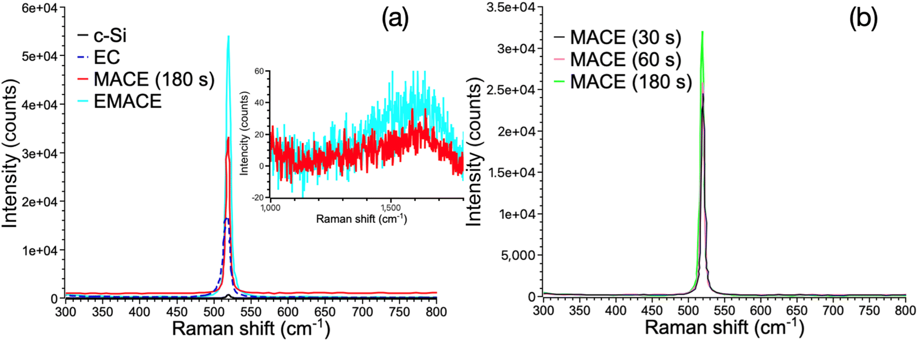 | ||
| Fig. 5 Raman spectra for crystalline (c-Si) and porous silicon with and without nickel prepared by different methods (a) and for Ni-decorated porous silicon prepared by MACE method with varying times of etching (b). Raman signals from carbon bonds-related areas for the samples prepared by MACE (180 s) and EMACE methods are depicted in the inset in panel (a). | ||
A possible additional source of enhancement of the Raman peak is the doping of substitutional and interstitial single nickel atoms incorporated into the silicon matrix. Since a high rate of nickel absorption into the silicon has been reported in multiple experiments (see, for example ref. 48 and 49) the effect of the Ni-doping on the local electronic structure was studied. The modeling of substitutional (NiSi) and interstitial (Nii) defects has been carried out. The simulation details are the same as in our recent work.50 As shown in Fig. 6a and b. The electronic structure of substitutional nickel impurity has the same peak at the Fermi level as silver (see Fig. 6c). Since the silver nanostructures demonstrate enhancement of the Raman peak and SVG performance, an increase in the intensity of the Raman peak in the sample prepared by EMACE method with silver-like changes in local electronic structures in Ni-doped silicon matrix can be associated.
 | ||
| Fig. 6 The changes of the charge densities after incorporation of substitutional (a) and interstitial (b) nickel impurity. The yellow “clouds” correspond with an increase in the charge densities, and the cyan “clouds” correspond with a decrease in the charge densities. Panel (c) depicts partial densities of states for metallic silver, substitutional, and interstitial nickel impurities in a silicon matrix. | ||
To check the possibility of the carbon nucleation reported for cz-Si51 and the formation of some ordered carbon structures, the Raman spectra in the range between 1000 and 2000 cm−1 in the sample with the most significant carbon content (EMACE) have been taken. Results of measurements demonstrate the presence of some carbon–carbon bonds in the spectra (see inset in Fig. 5a) without typical for various layered carbon structures D and G peaks.52 Based on the tiny magnitude of the Raman signal from these carbon structures and the absence of peaks corresponding with ordered carbon structure, these carbon structures provide no effects on enhancing the Raman signal.
The next step of our studies is to check the samples' vaporization performance. Shapes of the water droplets depict a hydrophilic character of the surface area for all studied samples (see Fig. S2†). Fig. 7a and b shows the formation of bubbles on the surface of freshly prepared samples at room temperature. The vaporizing performance for the samples fabricated by EC, MACE, and EMACE methods is about 4.4, 4.6, and 5.2 kg m−2 h−1, respectively (see Fig. 7c). Note that the latter value is an approach to the maximal reported performance of SVG devices (5.7 kg m−2 h−1).15 Since the intensity of the Raman peak of the sample fabricated by the MACE method is almost two times larger than for the samples prepared by the EC method (33000 counts vs. 17000 counts), the nearly identical vaporization performance of these samples demonstrates the influence of other factors on this property. The different shapes of the surfaces of these samples (see Fig. 2a and d) and different degrees of structural disorder (see Fig. 4a and c). The samples prepared by the EMACE method demonstrate higher porosity and a more significant number of defects than those prepared by the MACE method (see Fig. 2). To evaluate the wettability of the samples, water droplets were formed on the surfaces and removed after one minute. After this, the samples were weighted. The measured weight of the water remaining in the samples after brief surface wetting is 16.5, 5.9, and 17.3 g m−2 for the samples prepared by EC, MACE (180 s), and EMACE methods, respectively. Thus, the discussed differences could be associated with different wetting patterns, which are also essential for SVG performance.53
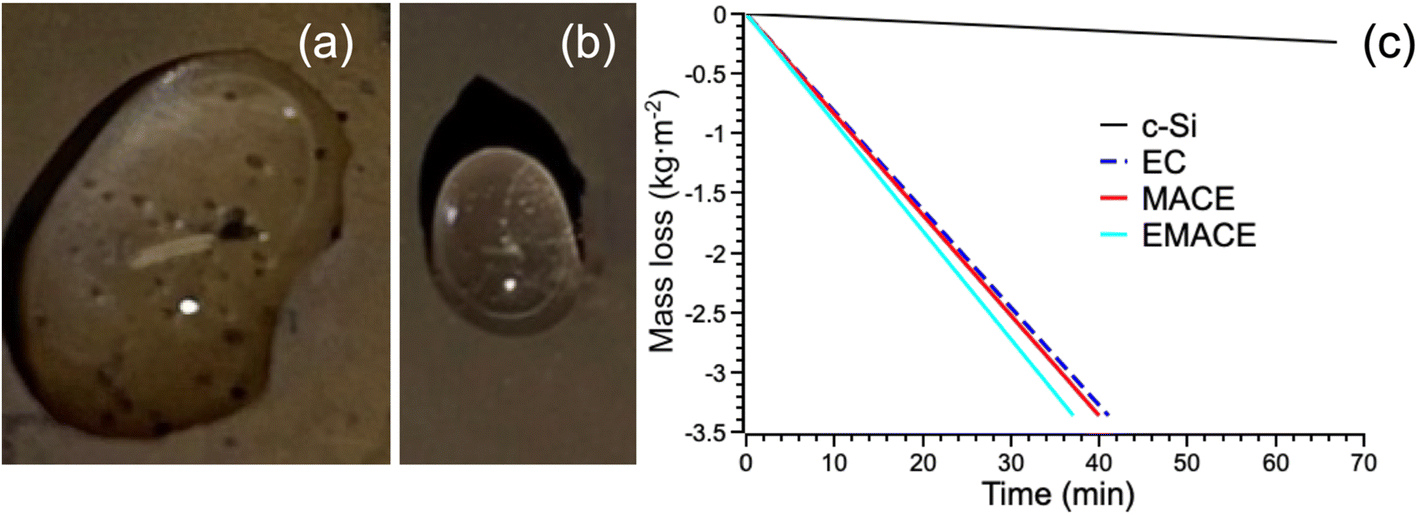 | ||
| Fig. 7 Photographic images of the bubbles formed in water on the surface of samples prepared by EMACE (a) and MACE (b) methods. Panel (c) shows mass variation over time at room temperature over silicon-based substrates fabricated by various methods. | ||
4. Conclusions
This work presented the fabrication of centimeter-size porous silicon with and without Ni-doping using a one-step process. Microscopy demonstrates various morphologies of the samples prepared by different methods. The metal-assisted chemical etching (MACE) samples exhibit a lower porosity level. On the contrary, the samples prepared by electrochemical etching (EC) and electrochemical metal-assisted etching (EMACE) have rod-like morphology. XRD measurements also demonstrate differences between these two types of morphology: EC samples exhibit a high level of crystallinity, in contrast to samples prepared by EC and EMACE methods. Later, it reflects the lack of short-distance orders. Raman spectra show dramatic enhancement in the magnitude of the signal. EMACE sample demonstrates the most significant increase in the Raman signal intensity. This effect can be partially associated with silver-like features in the electronic structures in Ni-doped areas. Drops of water were placed on the surface of all studied samples to evaluate solar vapor generation performance. The visible naked-eye vapor bubbles formed inside these water drops were observed in the MACE and EMACE samples prepared. The estimated vaporization performance of studied samples varies from 4.4 kg m−2 h−1 for EC samples up to 5.2 kg m−2 h−1 for EMACE samples. The numbers above are reported for the various systems prepared by more sophisticated techniques and more than four times more significant than previously reported for silicon-based SVGs prepared in smaller quantities using more sophisticated techniques (0.9–1.1 kg m−2 h−1).25,26 Thus, simple one-step methods for large-scale manufacturing of centimeter-size from cz-Si are prospective for developing efficient solar vapor generators for industrial manufacturing. Further developments in this direction required studies of the effects of aging, harsh environments, and water salinity on the stability and performance of tissue kind of SVG.Data availability
Data for this article, including results of XRD and Raman measurements, are available at Science Data Bank at https://doi.org/10.57760/sciencedb.17873.Conflicts of interest
There are no conflicts to declare.Acknowledgements
All authors acknowledge the support of the Science Committee of the Ministry of Science and Higher Education of the Republic of Kazakhstan (Grant No. BR21881954). The authors also thank L. Khamkash, K. Rustembekkyzy, and E. Vdovichenko for their help with SEM, Raman, and XRD measurements.References
- J. Liang, H. Liu, J. Yu, L. Zhou and J. Zhu, Plasmon-enhanced solar vapor generation, Nanophot, 2019, 8, 771–786, DOI:10.1515/nanoph-2019-0039.
- J. M. Gordon and H. T. Chua, Thermodynamic perspective for the specific energy consumption of seawater, Desalination, 2019, 386, 13–18, DOI:10.1016/j.desal.2016.02.030.
- A. Polman, Solar steam nanobubbles, ACS Nano, 2013, 7, 15–18, DOI:10.1021/nn305869y.
- C. Zhang, P. Xiao, F. Ni, Y. Yang, J. Gu, L. Zhang, J. Xia, Y. Huang, W. Wang and T. Chen, Programmable Interface Asymmetric Integration of Carbon Nanotubes and Gold Nanoparticles toward Flexible, Configurable, and Surface-Enhanced Raman Scattering Active All-In-One Solar-Driven Evaporators, Energy Technol., 2019, 7, 1900787, DOI:10.1002/ente.201900787.
- M. J. Margeson and M. Dasog, Plasmonic metal nitrides for solar-driven water evaporation, Environ. Sci.:Water Res. Technol., 2020, 6, 3169–3177, 10.1039/D0EW00534G.
- B. S. Joo, I. S. Kim, I. K. Han, H. Ko, J. G. Kang and G. Kang, Plasmonic silicon nanowires for enhanced heat localization and interfacial solar steam generation, Appl. Surf. Sci., 2022, 583, 152563, DOI:10.1016/j.apsusc.2022.152563.
- S. Son, J. Park, S. Ju, D. Huh, J. Jun, K. Kim, P.-H. Jung and H. Lee, Broadband Meta-Absorber with Au/Ni Core–Shell Nanowires for Solar Vapor Generator, Adv. Sustainable Syst., 2012, 5, 2000217, DOI:10.1002/adsu.202000217.
- C. Chang, C. Yang, Y. Liu, P. Tao, C. Song, W. Shang, J. Wu and T. Deng, Efficient Solar-Thermal Energy Harvest Driven by Interfacial Plasmonic Heating-Assisted Evaporation, ACS Appl. Mater. Interfaces, 2016, 8, 23412–23418, DOI:10.1021/acsami.6b08077.
- M. S. Zielinski, J.-W. Choi, T. La Grange, M. Modestino, S. M. H. Hashemi, Y. Pu, S. Birkhold, J. A. Hubbel and D. Psaltis, Hollow Mesoporous Plasmonic Nanoshells for Enhanced Solar Vapor Generation, Nano Lett., 2016, 16, 2159–2167, DOI:10.1021/acs.nanolett.5b03901.
- S. Chen, Z. Sun, W. Xiang, C. Shen, Z. Wang, Xi. Jia, J. Sun and C. J. Liu, Plasmonic wooden flower for highly efficient solar vapor generation, Nano Energy, 2020, 76, 104998, DOI:10.1016/j.nanoen.2020.104998.
- Y. Shi, C. Zhang, Y. Wang, Y. Cui, Q. Wang, G. Liu, S. Gao and Y. Yuan, Plasmonic silver nanoparticles embedded in flexible three-dimensional carbonized melamine foam with enhanced solar-driven water evaporation, Desalination, 2021, 507, 115038, DOI:10.1016/j.desal.2021.115038.
- C. Zhao, H. Sun, J. Wang and H. Yang, Light-induced enhanced phase change process of plasmonic nanofluids: The reduction of the latent heat of vaporization, Appl. Therm. Eng., 2024, 240, 122140, DOI:10.1016/j.applthermaleng.2023.122140.
- B. Sharma and M. K. Rabinal, Plasmon based metal-graphene nanocomposites for effective solar vaporization, J. Alloys Compd., 2017, 690, 57–62, DOI:10.1016/j.jallcom.2016.07.330.
- W. Wang, X. Yan, J. Geng, N. Zhao, L. Liu, T. Vogel, Q. Guo, L. Ge, B. Luo and Y. Zhao, Engineering a Copper@Polypyrrole Nanowire Network in the Near Field for Plasmon-Enhanced Solar Evaporation, ACS Nano, 2021, 15, 16376–16394, DOI:10.1021/acsnano.1c05789.
- L. Zhou, Y. Tan, J. Wang, W. Xu, Y. Yuan, W. Cai, S. Zhu and J. Zhu, 3D self-assembly of aluminium nanoparticles for plasmon-enhanced solar desalination, Nat. Photonics, 2016, 10, 393–398, DOI:10.1038/nphoton.2016.75.
- Y. Wang, L. Zhang and P. Wang, Self-Floating Carbon Nanotube Membrane on Macroporous Silica Substrate for Highly Efficient Solar-Driven Interfacial Water Evaporation, ACS Sustainable Chem. Eng., 2016, 4, 1223–1230, DOI:10.1021/acssuschemeng.5b01274.
- G. Ni, N. Miljkovic, H. Ghasemi, X. Huang, S. V. Boriskina, C.-T. Lin, J. Wang, Y. Xu, Md. M. Rahman, T. Zhang and G. Chen, Volumetric solar heating of nanofluids for direct vapor generation, Nano Energy, 2015, 17, 290–301, DOI:10.1016/j.nanoen.2015.08.021.
- S. Liu, C. Huang, X. Luo and Z. Rao, High-performance solar steam generation of a paper-based carbon particle system, Appl. Therm. Eng., 2018, 142, 566–572, DOI:10.1016/j.applthermaleng.2018.07.032.
- M. Gao, L. Zhu, C. K. Peh and G. W. Ho, Solar absorber material and system designs for photothermal water vaporization towards clean water and energy production, Energy Environ. Sci., 2019, 12, 841–864, 10.1039/C8EE01146J.
- S. Yu, Y. Gu, X. Chao, G. Huang and D. Shou, Recent advances in interfacial solar vapor generation: clean water production and beyond, J. Mater. Chem. A, 2023, 11, 5978–6015, 10.1039/D2TA10083E.
- M. S. Schmidt, J. Hübner and A. Boisen, Large Area Fabrication of Leaning Silicon Nanopillars for Surface Enhanced Raman Spectroscopy, Adv. Mater., 2012, 24, OP11–OP18, DOI:10.1002/adma.201103496.
- P. A. Dmitriev, D. G. Baranov, V. A. Milichko, S. V. Makarov, I. S. Mukhin, A. K. Samusev, A. E. Krasnok, P. A. Belov and Y. S. Kivshar, Resonant Raman scattering from silicon nanoparticles enhanced by magnetic response, Nanoscale, 2016, 8, 9721–9726, 10.1039/C5NR07965A.
- H. Wang, X. Jiang, S.-T. Lee and Y. He, Silicon Nanohybrid-based Surface-enhanced Raman Scattering Sensors, Small, 2014, 10, 4455–4468, DOI:10.1002/smll.201401563.
- M. Khorasaninejad, J. Walia and S. S. Saini, Enhanced first-order Raman scattering from arrays of vertical silicon nanowires, Nanotechnology, 2012, 23, 275706, DOI:10.1088/0957-4484/23/27/275706.
- B. S. Joo, I. S. Kim, I. K. Han, H. Ko, J. G. Kang and G. Kang, Plasmonic silicon nanowires for enhanced heat localization and interfacial solar steam generation, Appl. Surf. Sci., 2022, 583, 152563, DOI:10.1016/j.apsusc.2022.152563.
- S. Cheng, Z. Yu, Z. Lin, L. Li, Y. Li and Z. Mao, A lotus leaf like vertical hierarchical solar vapor generator for stable and efficient evaporation of high-salinity brine, Chem. Eng. J., 2020, 401, 126108, DOI:10.1016/j.cej.2020.126108.
- A. M. Al-Syadi, M. Faisal, A. M. El-Toni, A. Khan, M. Jalalah, S. A. Alsareii and F. A. Harraz, Surface-enhanced Raman scattering (SERS) active substrate from gold nanoparticle-coated porous silicon for sensitive detection of horseradish peroxidase enzyme, Mater. Chem. Phys., 2022, 281, 125931, DOI:10.1016/j.matchemphys.2022.125931.
- P.-S. Yang, Y.-T. Yin, P.-C. Lin, L.-Y. Chen and M.-J. Chen, High chemical resistance and Raman enhancement in Ag/Al2O3 core-shell plasmonic nanostructures tailored by atomic layer deposition, Mater. Chem. Phys., 2019, 223, 441–446, DOI:10.1016/j.matchemphys.2018.11.009.
- T.-H. Chang, K.-W. Chuang, Y.-C. Chang and C.-M. Chou, Optimizing and improving the growth of Ag nanoparticles decorated on the silicon pyramid for surface-enhanced Raman spectroscopy, Mater. Chem. Phys., 2022, 280, 125823, DOI:10.1016/j.matchemphys.2022.125823.
- H. Zou, G. Ren, M. Shang and W. Wang, One-step, seedless, fabrication of three-dimensional gold meso-flowers (3D-AuMFs) with high activities in catalysis and surface-enhanced Raman scattering, Mater. Chem. Phys., 2016, 176, 115–120, DOI:10.1016/j.matchemphys.2016.03.039.
- A. M. Alwan, D. A. Hashim and M. Jawad, Optimizing of porous silicon alloying process with bimetallic nanoparticles, Gold Bull., 2018, 51, 175–184, DOI:10.1007/s13404-018-0242-3.
- L. A. Wali, A. B. Dheyab and A. M. Alwan, Study the influence of shell thickness in bimetallic Ag core&Au shell configurations integrated in bare Si PN junction solar cells, Mater. Sci. Eng., B, 2023, 288, 116210, DOI:10.1016/j.mseb.2022.116210.
- A. B. Dheyab, L. A. Wali, A. M. Alwan and I. A. Naseef, Perfect incorporation of AuNPs on the p–n+ porous silicon for highly-efficient solar cells, Optik, 2019, 198, 163317, DOI:10.1016/j.ijleo.2019.163317.
- V. Lehmann and U. Gösele, Porous silicon formation: A quantum wire effect, Appl. Phys. Lett., 1991, 58, 856, DOI:10.1063/1.104512.
- H. Hana, Z. Huang and W. Lee, Metal-assisted chemical etching of silicon and nanotechnology applications, Nano Today, 2014, 9, 271–304, DOI:10.1016/j.nantod.2014.04.013.
- H. S. Jang, H.-J. Choi, B.-Y. Oh and J. H. Kim, Combinational Approach of Electrochemical Etching and Metal-Assisted Chemical Etching for p-Type Silicon Wire Formation, Electrochem. Solid-State Lett., 2011, 14, D5, DOI:10.1149/1.3504127.
- E. Torralba, S. L. Gall, R. Lachaume, V. Magnin, J. Harari, M. Halbwax, J.-P. Vilcot, C. Cachet-Vivier and S. Bastide, Tunable Surface Structuration of Silicon by Metal Assisted Chemical Etching with Pt Nanoparticles under Electrochemical Bias, ACS Appl. Mater. Interfaces, 2016, 8, 31375–31384, DOI:10.1021/acsami.6b09036.
- A. A. Leonardi, M. J. Lo Faro and A. Irrera, Silicon Nanowires Synthesis by Metal-Assisted Chemical Etching: A Review, Nanomaterials, 2021, 11, 383, DOI:10.3390/nano11020383.
- M. Scarlete, Mechanism of Carbon and Oxygen Incorporation in Silicon Single Crystals Grown by the Czochralski (Cz) Technique, J. Electrochem. Soc., 1992, 139, 1207, DOI:10.1149/1.2069368.
- X. Yu, J. Chen, X. Ma and D. Yang, Impurity engineering of Czochralski silicon, Mater. Sci. Eng., R, 2013, 74, 1–33, DOI:10.1016/j.mser.2013.01.002.
- Y. Wang, Y. Li, G. Wang, J. Zhu, H. Yang, L. Jin, S. Hu and H. Hu, In-situ catalytic upgrading of coal pyrolysis volatiles over red mud-supported nickel catalysts, Fuel, 2022, 324, 124742, DOI:10.1016/j.fuel.2022.124742.
- D. W. Boukhvalov, D. A. Zatsepin, D. Y. Biryukov, Y. V. Shchapova, N. V. Gavrilov and A. F. Zatsepin, Structural, electronic, and optical properties of 6H-SiC layers synthesized by implantation of carbon ions into silicon, Appl. Surf. Sci., 2024, 666, 160379, DOI:10.1016/j.apsusc.2024.160379.
- S. M. Abed, S. M. Mohammad, Z. Hassan, A. Muhammad, S. Rajamanickam and K. Ali, Comparative study of UV-ZnO NRs photodetectors based on seeded porous silicon by RF-sputtering and drop-casting methods, J. Mater. Sci.: Mater. Electron., 2022, 33, 26322–26342, DOI:10.1007/s10854-022-09315-1.
- C. A. C. Abdullah, D. F. A. Razak, M. B. Md. Yunus and M. Z. M. Yusoff, Structural and Optical Properties of N-Type and P-Type Porous SiliconProduced at Different Etching Time, Int. J. Electroactive Mater., 2019, 7, 28–37 Search PubMed . https://www.electroactmater.com/index.php/volume-7-2019?id=60%26subid=322.
- M. Nabil and H. Motaweh, Synthesis, Antimicrobial, Antioxidant and Docking Study of Studying The Wetting agent Impact in The Porous Silicon Production, Egypt. J. Chem., 2020, 63, 1849–1855, DOI:10.21608/ejchem.2019.16971.2039.
- R. Venkatesan, J. Mayandi, J. M. Pearce and V. Venkatachalapathy, Influence of metal assisted chemical etching time period on mesoporous structure in as-cut upgraded metallurgical grade silicon for solar cell application, J. Mater. Sci.: Mater. Electron., 2019, 30, 8676–8685, DOI:10.1007/s10854-019-01191-6.
- K. Tynyshtykbayev, Ch. Spitas, K. Kostas and Z. Insepov, Porous Silicon Skeleton as Catalysts for Hydrocarbon Decomposition at Low Temperature Synthesis of Graphene Nanocomposites, ECS J. Solid State Sci. Technol., 2021, 10, 013009, DOI:10.1016/10.1149/2162-8777/abdd86.
- A. R. Neale, Y. Jin, J. Ouyang, S. Hughes, D. Hesp, V. Dhanak, G. Dearden, S. Edwardson and L. J. Hardwick, Electrochemical performance of laser micro-structured nickel oxyhydroxide cathodes, J. Power Sources, 2014, 271, 42–47, DOI:10.1016/j.jpowsour.2014.07.167.
- N. Yarykin and J. Weber, Evidence for room-temperature in-diffusion of nickel into silicon, Appl. Phys. Lett., 2016, 109, 102101, DOI:10.1063/1.4962394.
- D. W. Boukhvalov, K. A. Abdullin, T. S. Turmagambetov, A. K. Shongalova, I. S. Nevmerzhitskiy and A. S. Serikkanov, Effect of transition metals co-dopant on eliminating boron and phosphorous impurities from silicon, Sep. Purif. Technol., 2024, 334, 126107, DOI:10.1016/j.seppur.2023.126107.
- M. Kanamori and H. Tsuya, Microdefects Formed in Carbon-Doped CZ Silicon Crystals by Oxygen Precipitation Heat Treatment, Jpn. J. Appl. Phys., 1985, 24, 557, DOI:10.1143/JJAP.24.557.
- L. Bokobza, J.-L. Bruneel and M. Couzi, Raman Spectra of Carbon-Based Materials (from Graphite to Carbon Black) and of Some Silicone Composites, C-J. Carbon Res., 2015, 1, 77–94, DOI:10.3390/c1010077.
- J. Yin, J. Xu, W. Xu, S. Liu, W. Li, Z. Fang, C. Lu and Z. Xu, Tuning the wettability of solar absorbers towards high-efficiency solar vapor generation, Appl. Therm. Eng., 2021, 183, 116224, DOI:10.1016/j.applthermaleng.2020.116224.
Footnote |
| † Electronic supplementary information (ESI) available. See DOI: https://doi.org/10.1039/d5ra00703h |
| This journal is © The Royal Society of Chemistry 2025 |