
 Open Access Article
 This Open Access Article is licensed under a Creative Commons Attribution-Non Commercial 3.0 Unported Licence
Examining the contribution of charge transport layers to boost the performance over 26% in Sr3PCl3 absorber-based bifacial perovskite solar cells
Asadul Islam Shimul *a,
Avijit Ghoshb,
Swarna Rani Sarkera and
Huriyyah A. Alturaific
*a,
Avijit Ghoshb,
Swarna Rani Sarkera and
Huriyyah A. Alturaific
aDepartment of Electrical and Electronic Engineering, Bangabandhu Sheikh Mujibur Rahman Science and Technology University, Gopalganj-8100, Bangladesh. E-mail: shimul7246@gmail.com
bDepartment of Electrical and Electronic Engineering, Begum Rokeya University, Rangpur-5400, Bangladesh
cDepartment of Chemistry, Faculty of Science, King Khalid University, PO Box 9004, Abha, 61413, Saudi Arabia
First published on 10th March 2025
Abstract
Strontium phosphorus chloride (Sr3PCl3) presents a promising option for photovoltaic (PV) applications due to its distinctive optical, electrical, and structural characteristics. This research uses density functional theory (DFT) to examine its structural stability and optoelectronic properties. The PV performance of Sr3PCl3-based cell designs was examined, utilizing an electron transport layer (ETL) of ZnO and four different hole transport layers (HTLs): Cu2O, CBTS, MoO3, and CuI. Essential parameters, including band alignment, layer thickness, defect density, doping concentration, interface defect density, carrier concentration, and generation-recombination rates, were consistently assessed via numerical simulations utilizing SCAPS-1D software. The findings indicated that the Cu2O HTL structure attained the highest power conversion efficiency (PCE) of 26.67%, with an open-circuit voltage (VOC) of 1.3 V, a short-circuit current density (JSC) of 22.79 mA cm−2 and a fill factor (FF) of 89.9%. The CBTS, MoO3, and CuI HTL designs attained PCEs of 26.39%, 24.86%, and 21.78%, respectively. To enhance device performance, the bifacial mode was investigated, and the PV efficacy of the proposed PSC structure was examined. Among these, the Cu2O-based structure shows the highest performance, attaining a bifacial factor of 87.21%, a bifacial gain of 16.74% and bifacial efficiency of 31.07%. These findings provide significant insights and propose a viable approach for the advancement of economic and excellent performance Sr3PCl3-based perovskite solar cells.
1 Introduction
The rising worldwide energy consumption is driven by population increase, rapid technical progress, and the development of previously neglected areas. Forecasts suggest that energy consumption may reach an astounding 30 terawatts (TW) by 2050.1,2 The increasing demand, along with the exhaustion of conventional energy resources, underscores the necessity of discovering and adopting sustainable alternatives in the energy sector.3 The application of perovskite materials represents a significant improvement in solar cell technologies within the field of renewable energy.4,5 These materials can substantially improve the efficiency of solar systems. Currently, there is an increasing emphasis on exploring inorganic perovskite compounds as efficient absorber materials for next-generation PV cells.6,7Among the most promising prospects in this field are perovskites of the A3MX3 group (where “X” denotes a charged particle (anion), and “A” and “M” signify cations).8 Recent breakthroughs in the integration of organic–inorganic hybrid PSCs have resulted in notable improvements, such as increased charge-carrier mobility, extended carrier lifetimes, diminished trap densities, and reduced exciton binding energies.9 These gains are ascribed to enhanced material control issues like volatility, and thermal instability persists as substantial obstacles.
The inorganic perovskite Sr3PCl3 has garnered considerable interest as a potential solution to the stability challenges typically encountered with traditional PSCs. Its principal advantage lies in its exceptional compositional stability and thermal resistance, rendering it significantly more durable under environmental stressors such as moisture and elevated temperatures than conventional halide perovskites. Sr3PCl3 features an adjustable bandgap of roughly 1.7 eV, making it very beneficial for incorporation into high-performance tandem solar cells, since it can efficiently capture energy across an extended range of the solar spectrum.10 The location of this bandgap enables it to augment other perovskite materials, hence improving total cell efficiency in tandem arrangements. Regarding operational stability, Sr3PCl3 has exceptional performance. Over the last ten years, the PCE of halide PSCs has increased from 2.9% to more than 25%, driven by improvements in material synthesis.11,12 Nevertheless, structural instability, particularly the shift from active black to inactive yellow phases, continues to pose a significant challenge, adversely affecting both efficiency and durability.13,14 Various strategies, including optimizing surface energy, doping, and controlling particle size, have been employed to tackle this problem Doping Sr3PCl3 into the perovskite lattice has demonstrated a substantial improvement in both stability and efficiency.15 When integrated with suitable ETLs, these strategies improve the stability and efficiency of halide PSCs,16–18 approaching the efficacy of conventional lead-based perovskites. This enhancement results from the material's exceptional charge transport characteristics, which are additionally augmented by doping techniques. Notwithstanding these encouraging outcomes, the complete potential of Sr3PCl3-based PSCs is still under investigation, since obstacles persist in optimizing band alignment, modifying layer thickness, and precisely changing doping concentrations in the active layers.
Zinc oxide (ZnO) has been prominent among ETLs due to its superior compatibility with perovskite materials. The material's extensive bandgap, elevated electron mobility, and visibility spectrum transparency facilitate effective charge transport and collection.19 ZnO improves perovskite-to-electrode electron transport, hence augmenting the overall performance of the device. Furthermore, wide bandgap semiconductors are widely preferred for their capacity to facilitate charge transfer in PSCs. Notwithstanding the considerable advancements made with ZnO and other ETLs, obstacles persist in actualizing the whole potential of Sr3PCl3-based PSCs. These issues encompass optimizing band alignment, reducing defect density, and establishing stable interfaces between absorber layers and ETL. Advanced interface engineering methodologies, including the integration of hybrid ETLs and the application of interfacial doping, are being investigated to resolve these challenges.20,21
Although AMX3 perovskites have led to substantial enhancements in PSC efficiency, reporting values of 24.55% for AMX3-based cells, 33.7% for perovskite–silicon tandem cells, and 28.6% for all-perovskite tandem cells investigation into A3MX3 perovskite structures remains nascent.22,23 Theoretical studies employing methodologies such as DFT and SCAPS-1D have predominantly concentrated on materials such as Sr3PI3, Sr3SbI3, Sr3AsCl3, and Sr3NCl3.24–27 These materials demonstrate PCE between 25 and 30%. Their high-symmetry crystalline structures and octahedral networks facilitate superior photovoltaic transitions while also being non-toxic and environmentally sustainable. The potential of A3MX3 perovskites resides in their structural versatility and capacity to attain ideal band alignments. This versatility facilitates the optimization of optical and electrical properties, hence improving charge transfer and light absorption. Sr3PCl3 is a promising material for PSCs owing to its lead-free formulation and enhanced resilience to moisture and heat degradation. It provides superior efficiency and extended longevity relative to conventional perovskites, which frequently exhibit toxicity and environmental susceptibility. Its distinctive atomic configuration improves charge transmission and stability, rendering it a more sustainable and dependable option for solar energy applications.
Research is also concentrating on HTLs to enhance device performance. Materials including Cu2O, MoO3, CBTS, and CuI are under examination for their ability to improve charge extraction and reduce recombination losses. Organic HTLs like PTAA and PCBM are preferred due to their ideal energy alignment with perovskite layers and excellent hole mobility.28 Nonetheless, they encounter difficulties pertaining to expenses, consistency in operational circumstances, and fluctuations in production. Conversely, inorganic HTLs like Cu2O and CBTS provide enhanced stability and reduced prices, rendering them appealing alternatives.29 Hybrid HTLs, which integrate organic and inorganic materials, are developing as a promising method to amalgamate the benefits of both material categories.30 These hybrid materials seek to enhance charge transport characteristics while ensuring stability and cost-efficiency.
This paper provides an in-depth examination of the structural, optical, and electrical characteristics of the unique compound Sr3PCl3 in conjunction with four different HTLs: Cu2O, MoO3, CBTS, and CuI. To improve the optoelectronic properties of the Sr3PCl3 absorber and optimize its interaction with HTLs. Advanced computational methods, like SCAPS-1D and DFT, are utilized to evaluate diverse interface properties. The PV performance of solar cells employing Sr3PCl3 as the absorber material alongside the HTLs. Essential parameters such as layer thickness, interface defect density, bulk defect density, doping density, operating temperature, generation and recombination rates, current density–voltage (J–V), and quantum efficiency (QE) characteristics are thoroughly examined. The investigation underscores the cumulative impact of these factors on device efficiency. Finally, we assess the viability of the suggested four PSC architectures for application as bifacial solar cells, with the objective of attaining improved PV performance. The study closes by delineating optimal conditions that enhance the efficacy of Sr3PCl3-based PSCs, providing significant insights for future progress in PV technology.
2 Computational details
The optoelectronic properties of the Sr3PCl3 perovskite structure were explored using first-principles DFT computations.31,32 These simulations were conducted inside the Cambridge Serial Total Energy Package (CASTEP) framework, applying the plane wave pseudopotential technique.33 The exchange–correlation energy was addressed using the Perdew–Burke–Ernzerhof (PBE) functional, a widely adopted formulation under the Generalized Gradient Approximation (GGA), ensuring an accurate depiction of system interactions.34 To efficiently describe electron-ion interactions, the ultrasoft pseudopotential approach was utilized, enabling a compromise between computing efficiency and precision. Geometry optimization was undertaken to discover the most stable crystal arrangement, where the system's structure adjusts to the lowest energy state under periodic boundary conditions. This stage is crucial for replicating the inherent behavior of the crystal in equilibrium conditions. The Brillouin zone sampling uses a Monkhorst–Pack k-point mesh of 12 × 12 × 12 to achieve accuracy while retaining computational practicality. The plane wave expansion was set with a cutoff energy of 550 eV, ensuring the convergence of total energy estimates. The Broyden–Fletcher–Goldfarb–Shanno algorithm was employed for structural optimization, serving as a reliable technique for energy minimization that diminishes internal pressures and external stresses, ensuring a stable crystal configuration.35 Additionally, solar cell performance was studied using SCAPS-1D, simulating electrostatic potential and steady-state electron and hole transport through continuity equations.36,37 These calculations offer an in-depth comprehension of the proposed solar cell designs and their optoelectronic efficacy.3 Result and discussion
3.1 Structural characteristics
Sr3PCl3 is categorized within the cubic crystal system, specifically belonging to the space group Pm![[3 with combining macron]](https://www.rsc.org/images/entities/char_0033_0304.gif) m (no. 221), as depicted in Fig. 1(a). The unit cell contains seven atoms: three strontium (Sr) atoms at the 3c positions (0, 0.5, 0.5), one phosphorus (P) atom located at the 1b position (0.5, 0.5, 0.5), and three chlorine (Cl) atoms at the 3d positions (0.5, 0, 0).38 The electronic band structure of the material is represented along a defined path in the Brillouin Zone, traversing the high-symmetry points X–R–M–Γ–R. This representation illustrates periodic band diagrams essential for comprehending its electronic properties. The lattice parameter has been optimized to 6.043 Å, indicating a stable and energetically favorable configuration of the material. The properties collectively underscore the structural and electronic sophistication of Sr3PCl3. The stability and formation probability of Sr3PCl3 perovskite structure can be evaluated using the Goldschmidt tolerance factor, t, a recognized metric for assessing perovskite geometries. The tolerance factor is expressed in eqn (1).
m (no. 221), as depicted in Fig. 1(a). The unit cell contains seven atoms: three strontium (Sr) atoms at the 3c positions (0, 0.5, 0.5), one phosphorus (P) atom located at the 1b position (0.5, 0.5, 0.5), and three chlorine (Cl) atoms at the 3d positions (0.5, 0, 0).38 The electronic band structure of the material is represented along a defined path in the Brillouin Zone, traversing the high-symmetry points X–R–M–Γ–R. This representation illustrates periodic band diagrams essential for comprehending its electronic properties. The lattice parameter has been optimized to 6.043 Å, indicating a stable and energetically favorable configuration of the material. The properties collectively underscore the structural and electronic sophistication of Sr3PCl3. The stability and formation probability of Sr3PCl3 perovskite structure can be evaluated using the Goldschmidt tolerance factor, t, a recognized metric for assessing perovskite geometries. The tolerance factor is expressed in eqn (1).
 | (1) |
 | ||
| Fig. 1 The (a) crystalline configuration and (b) solar cell architecture of Sr3PCl3 perovskite. | ||
3.2 Electronic characteristics
The electronic band structure and symmetry of key points in the Sr3PCl3 crystal were analyzed following structural optimization. Materials with a direct bandgap are essential for optoelectronic applications, as they improve light absorption and emission efficiency. The density of states (DOS) and band structure are crucial in defining the electronic properties of materials. The band structure of Sr3PCl3, illustrated in Fig. 2(a), is represented along the k-axis path X–R–M–Γ–R to investigate its cubic crystal symmetry. The Fermi level is set to zero to facilitate precise bandgap analysis, emphasizing the valence band maximum (VBM) and conduction band minimum (CBM) at the Γ (Gamma) point. Simulations indicate that Sr3PCl3 has a direct bandgap of about 1.65 eV, aligning with previous research.24–26,41 The specified bandgap value is optimal for photothermal and sustainable energy technologies, making Sr3PCl3 a promising candidate for photovoltaic (PV) and solar cell applications. | ||
| Fig. 2 An analysis of the Sr3PCl3 perovskite's (a) band structure, (b) PDOS, (c) dielectric function, and (d) absorption coefficient as functions of photon energy. | ||
A partial density of states (PDOS) analysis (Fig. 2(b)) evaluates the contributions of various atomic orbitals to the bandgap energy. This analysis demonstrates that Sr and P atoms, hybridized with Cl, are essential for sustaining the bandgap across the energy spectrum (−5 eV to 5 eV). The bonding in Sr3PCl3 is primarily covalent, characterized by notable electron charge transfer from Sr and P atoms to Cl atoms, attributed to differences in atomic states.
The PDOS plot additionally illustrates that the valence band (VB) is predominantly affected by the Cl-3p orbital, indicated by the green peaks contributions from P-3p (magenta) and Sr-3d (red) orbitals are also noted. The conduction band (CB) is primarily influenced by the Sr-3d orbital, with minor contributions from the Sr-5s orbital evident as reddish spikes. The total density of states (TDOS), indicated by the blue line, consolidates these contributions, demonstrating the distribution of states across the energy spectrum. This analysis elucidates the influence of atomic orbital hybridization and charge transfer mechanisms on the electronic properties of Sr3PCl3. The material exhibits a favorable bandgap, hybridized orbital interactions, and efficient charge transfer dynamics, positioning it as a strong candidate for energy-efficient technologies and advanced optoelectronic devices.
3.3 Optical characteristics
The investigation of optical properties entails a thorough evaluation of complex dielectric functions and absorption coefficients, which are crucial for determining a material's appropriateness for optoelectronic and PV cell applications. This study specifically investigates the optical properties of Sr3PCl3. The dielectric function, represented as ε(ω), consists of two components: the real part and the imaginary part. The components are represented mathematically in eqn (2), which elucidates the material's behavior in response to electromagnetic radiation.42| ε(ω) = ε1(ω) + iε2(ω) | (2) |
The real dielectric function, ε1(ω), provides significant insights into polarization and dispersion phenomena in Sr3PCl3. The Kramers–Kronig transformation43 is utilized to assess the material's true dielectric permittivity over a photon energy range reaching up to 30 eV, as depicted in Fig. 2(c). A critical parameter is ε1(0), denoting the dielectric constant at zero frequency, essential for comprehending the material's electrical behavior. The calculated value of ε1(0) for cubic Sr3PCl3 is 4.48. The evolution of ε1(ω) has substantial light absorption potential as it ascends from ε1(0) to its peak under optical stimulation, subsequently experiencing a rapid decrease. The positive values of ε1(ω) signify superior refractive characteristics and semiconducting behavior. The unique structural features of Sr3PCl3 are emphasized by its elevated dielectric constant peak, exceeding that of materials with reduced bandgaps. The imaginary component (ε2(ω)) is essential for analyzing optical absorption and energy storage via neutral charge excitations.44 Fig. 2(c) illustrates that ε2(ω) predominates a substantial segment of the absorption spectrum, with a peak value of 3.83 at an optical position associated with an energy absorption of roughly 6.56 eV. These peaks signify carrier migrations from VB to CB. Furthermore, for photon energies beyond 27.3 eV, ε2(ω) approaches zero, signifying negligible optical absorption and enhanced transparency.
A fundamental characteristic of Sr3PCl3 is its absorption coefficient, which quantifies the material's capacity to absorb light at various wavelengths. This attribute is crucial in assessing the efficacy of optical and electrical applications. The absorption coefficient is affected by various parameters, such as the material's crystalline structure, purity level, and sample thickness, all of which impact its optical performance. The absorption coefficient profile closely mirrors the attributes of the imaginary dielectric component. Visible light, a substantial segment of solar radiation, generally demonstrates an elevated absorption coefficient. Fig. 2(d) depicts the absorption coefficient of Sr3PCl3, highlighting two prominent absorption peaks in the energy ranges of 3–14 eV and 20–27 eV. The absorption peaks underscore the material's efficacy in absorbing photons over a wide energy range. Moreover, throughout the energy range of 2.5–10 eV range, the material demonstrates significant fluctuations in its absorption coefficient, rendering it adept at utilizing a substantial segment of the solar spectrum. While absorption in elevated energy ranges (12 eV and above) may not directly facilitate solar energy collection, it suggests potential for alternative applications, such as deep ultraviolet detectors. This extensive absorption enhances the PCE of solar cells by proficiently capturing a greater number of photons.
The correlation between the absorption coefficient and the optical bandgap (Eg) is articulated by the Tauc eqn (3),45,46
| (αE)n = A(E − Eg) | (3) |
3.4 Development and simulation of photovoltaic heterostructures
A series of photovoltaic heterostructures was developed, employing FTO/ZnO/Sr3PCl3 as the foundation and integrating several HTLs, including Cu2O, CBTS, MoO3, and CuI. The designs were classified as structure-I (FTO/ZnO/Sr3PCl3/Cu2O/Ni), structure-II (FTO/ZnO/Sr3PCl3/CBTS/Ni), structure-III (FTO/ZnO/Sr3PCl3/MoO3/Ni), and structure-IV (FTO/ZnO/Sr3PCl3/CuI/Ni). The simulation method entailed resolving essential equations, such as the continuity equations for electrons and holes, in conjunction with the electrostatic potential equations, all under steady-state conditions to ensure precise modeling of the material's behavior.36,37Fig. 1(a) depicts the crystal structure of Sr3PCl3, whereas Fig. 1(b) presents schematic representations of the heterostructures. Each solar cell consisted of a fluorine-doped tin oxide (FTO) front electrode, an n-type ZnO ETL, a strontium chloride perovskite absorber (Sr3PCl3), and heavily doped p-type HTLs such as Cu2O, CBTS, MoO3, or CuI. Nickel (Ni), possessing a work function of 5.5 eV, was employed as the back metal electrode owing to its superior conductivity, strong adherence to the layers, and compatibility with the hole transport layer, hence facilitating effective charge extraction. Moreover, nickel provides a cost-efficient substitute for pricier metals such as gold, while maintaining device efficacy. Fig. 3(a–d) depict the energy band diagram (EBD) for different structures. The evaluation of charge carrier generation was performed by examining the locations of the quasi-Fermi levels (Fn and Fp) during illumination. In perovskite absorbers, the valence band offset and conduction band offset are crucial in illustrating the influence of the electric field on the separation of photogenerated electron–hole pairs. The intrinsic potential and the corresponding electric field at the absorber/ETL contact markedly improve charge carrier separation efficiency. Nonetheless, many issues, like inadequate carrier transport, material imperfections, or inappropriate structural geometry, can hinder this process.
 | ||
| Fig. 3 EBD of the proposed four-device structure configurations (FTO/ZnO/Sr3PCl3/HTL/Ni) with different HTLs: (a) Cu2O, (b) CBTS, (c) MoO3, and (d) CuI. | ||
A thorough comprehension of charge carrier behavior requires an in-depth analysis of material characteristics, structural arrangements, and the fundamental processes of carrier formation, transit, and recombination. This can be accomplished by advanced modeling techniques, such as Poisson's equation, carrier continuity equations, and drift-diffusion equations. Simulation parameters for active materials such as FTO, ZnO, Sr3PCl3, and HTLs (e.g., Cu2O, CBTS, MoO3, and CuI) were obtained using a synthesis of DFT simulations and relevant literature insights. Table 1 shows the simulation parameter requirements for each layer, whereas Table 2 specifies interface characteristics at the absorber/ETL and HTL/absorber junction. The simulation assumes hole and electron thermal velocities of 107 cm s−1.49
| Parameters | FTO | ZnO | Sr3PCl3 | Cu2O | CBTS | MoO3 | CuI |
|---|---|---|---|---|---|---|---|
| a Signifies the variables parameter. | |||||||
| N (μm) | 0.1 | 0.05a | 1a | 0.1a | 0.1a | 0.1a | 0.1a |
| Eg (eV) | 3.6 | 3.3 | 1.65 | 2.2 | 1.9 | 3.0 | 3.1 |
| χ (eV) | 4 | 4 | 4.127 | 3.4 | 3.6 | 2.3 | 2.1 |
| ε (eV) | 9 | 9 | 4.489 | 7.5 | 5.4 | 18 | 6.5 |
| NV (cm−3) | 1.8 × 10¹⁹ | 1.8 × 10¹⁹ | 1 × 10¹⁹ | 1 × 10¹⁹ | 1.8 × 10¹⁹ | 2.2 × 10¹⁸ | 1 × 10¹⁹ |
| NC (cm−3) | 2.2 × 10¹⁸ | 3.7 × 10¹⁸ | 7.2 × 10¹⁸ | 2 × 10¹⁹ | 2.2 × 10¹⁸ | 1 × 10¹⁹ | 2.8 × 10¹⁹ |
| μn (cm2 V−1 s−1) | 100 | 100 | 80 | 200 | 30 | 210 | 100 |
| μh (cm2 V−1 s−1) | 20 | 25 | 25 | 8600 | 10 | 210 | 43.9 |
| ND (cm−3) | 1 × 10¹⁸ | 1 × 10¹⁸ | 0 | 0 | 0 | 0 | 0 |
| NA (cm−3) | 0 | 0 | 1 × 10¹⁷a | 1 × 10²⁰a | 1 × 10²⁰a | 1 × 10²⁰a | 1 × 10²⁰a |
| Nt (cm−3) | 1 × 10¹⁵ | 1 × 10¹⁵ | 1 × 10¹⁴ | 1 × 10¹⁵ | 1 × 10¹⁵ | 1 × 10¹⁵ | 1 × 10¹⁵ |
3.5 Optimizing the thickness of HTL, ETL, and absorber layers
Fig. 4(a) illustrates the effect of altering the thickness of the Sr3PCl3 absorber layer (from 400 to 2500 nm) on the performance optimization of solar cells utilizing four different HTLs (Cu2O, CBTS, MoO3, and CuI). Enhancing solar cell efficiency depends on achieving an exact equilibrium in the thickness of the absorber layer, as indicated in prior research.50 The selection of optimal thickness seeks to minimize material expenses while maintaining efficiency, informed by theoretical modeling and simulation. This thickness substantially affects the overall device performance, as it regulates essential phenomena such as recombination rates and carrier production. | ||
| Fig. 4 Effect of thickness changes on PV parameters across (a) absorber, (b) ETL, and (c) HTL layers. | ||
As the Sr3PCl3 layer thickness increases, recombination rates and carrier production significantly rise. The trends in VOC indicate that for Cu2O and CBTS-based structures, VOC exhibits a slight decline with increasing thickness, while for MoO3 and CuI-based structures, VOC remains nearly constant. Of these, Cu2O exhibits the highest VOC, with values declining slightly from 1.31 to 1.28 V. The JSC increases with thicker absorber layers due to improved light absorption. The reported increases in JSC for the four HTLs are substantial: Cu2O increases from 19.70 to 23.47 mA cm−2, CBTS from 19.87 to 23.45 mA cm−2, MoO3 from 19.51 to 23.19 mA cm−2, and CuI from 19.63 to 23.43 mA cm−2. These findings correspond with trends shown in prior studies.48,51 For Cu2O, CBTS, and MoO3-based structures, the FF is consistently 89.9%, 89.83%, and 89.52%, respectively.
In contrast, CuI demonstrates a minor reduction in FF, decreasing from 88.3% to 86.81%. The PCE of Sr3PCl3-based PSCs is significantly influenced by the crystallinity and defect density of the absorber layer. Efficient charge transport layers (ETLs and HTLs) and meticulously designed interfaces are crucial for reducing recombination losses. Improving structural architecture and optimizing production processes enhance charge extraction and light absorption. The PCE escalates with absorber thickness in all structures, with Cu2O exhibiting the greatest significant increase from 23.25% to 27.04%. Optimal solar cell performance is attained when the thickness of the absorber layer is adjusted to correspond with the diffusion length of charge carriers. For Sr3PCl3, an optimal thickness of approximately 1000 nm is deemed desirable, as it achieves a balance between effective light absorption and reduced recombination losses. Exceeding this thickness results in increased photon absorption and elevated recombination rates, hence diminishing overall performance. Simulations suggest that augmenting the thickness beyond 1000 nm results in diminishing returns, as the extended pathway for charge carriers heightens the probability of recombination prior to their collection. The peak PCE and JSC stay nearly unchanged beyond this thickness, underscoring the necessity for optimization to prevent superfluous material consumption while preserving high efficiency. This underscores the intricate equilibrium between enhancing light absorption and facilitating efficient charge carrier separation.
Fig. 4(b) examines the impact of ETL layer thickness on solar cell efficacy. Buffer or ETL layers are critical for effective and steady functioning, as they enable the flow of charge carriers (absorber to electrode). The thickness of the ETL layer influences interlayer contact resistance, light absorption, and carrier recombination.52 Large band gaps in reduced ETL layers allow nearly all incident photons to get through to the Sr3PCl3 layer, improving light absorption. Notwithstanding fluctuations in ETL thickness, the photovoltaic characteristics for the Cu2O, CBTS, MoO3, and CuI-based architecture remain predominantly consistent. The VOC values for these structures are 1.3, 1.29, 1.23, and 1.09 V; the JSC values are 22.79, 22.8, 22.55, and 22.78 mA cm2; the FF values are 89.9%, 89.83%, 89.52%, and 87.52%; and the PCE values are 26.67%, 26.39%, 24.86%, and 21.78%. The stability of these parameters indicates that the ETL performs its primary function, facilitating effective electron transport and extraction at an optimal thickness.
Fig. 4(c) examines the impact of varying HTL thickness (25–250 nm) for Cu2O, CBTS, MoO3, and CuI. HTLs promote charge carrier separation, facilitate transport, and reduce recombination losses, playing a vital role in solar cell efficiency. Inorganic HTLs like Cu2O surpass others (CBTS, CuI, and MoO3) due to their greater hole extraction capabilities, energy alignment, and stability. The back-surface field formed by the HTL further boosts carrier collection and minimizes recombination, an important component in advanced solar cell designs.
Within the examined thickness range, PCE values exhibit minimal variation: Cu2O ranges from 26.66% to 26.67%, CBTS from 26.38% to 26.40%, MoO3 from 24.85% to 24.87%, and CuI from 21.77% to 21.78%. Increased HTL thickness leads to increased series resistance, influencing FF and PCE. Beyond 100 nm, further increases in thickness offer minor performance differences.
So, optimizing the thickness of the absorber, ETL, and HTL are essential for maximum efficiency. Fig. 4(a–c) illustrate that thicknesses of 1000 nm, 50 nm, and 100 nm for the absorber, ETL, and HTL layers, respectively, provide cost-effective production while preserving optimal performance.
3.6 Impact of bulk defects and acceptor density in Sr3PCl3 absorber on PV efficiency
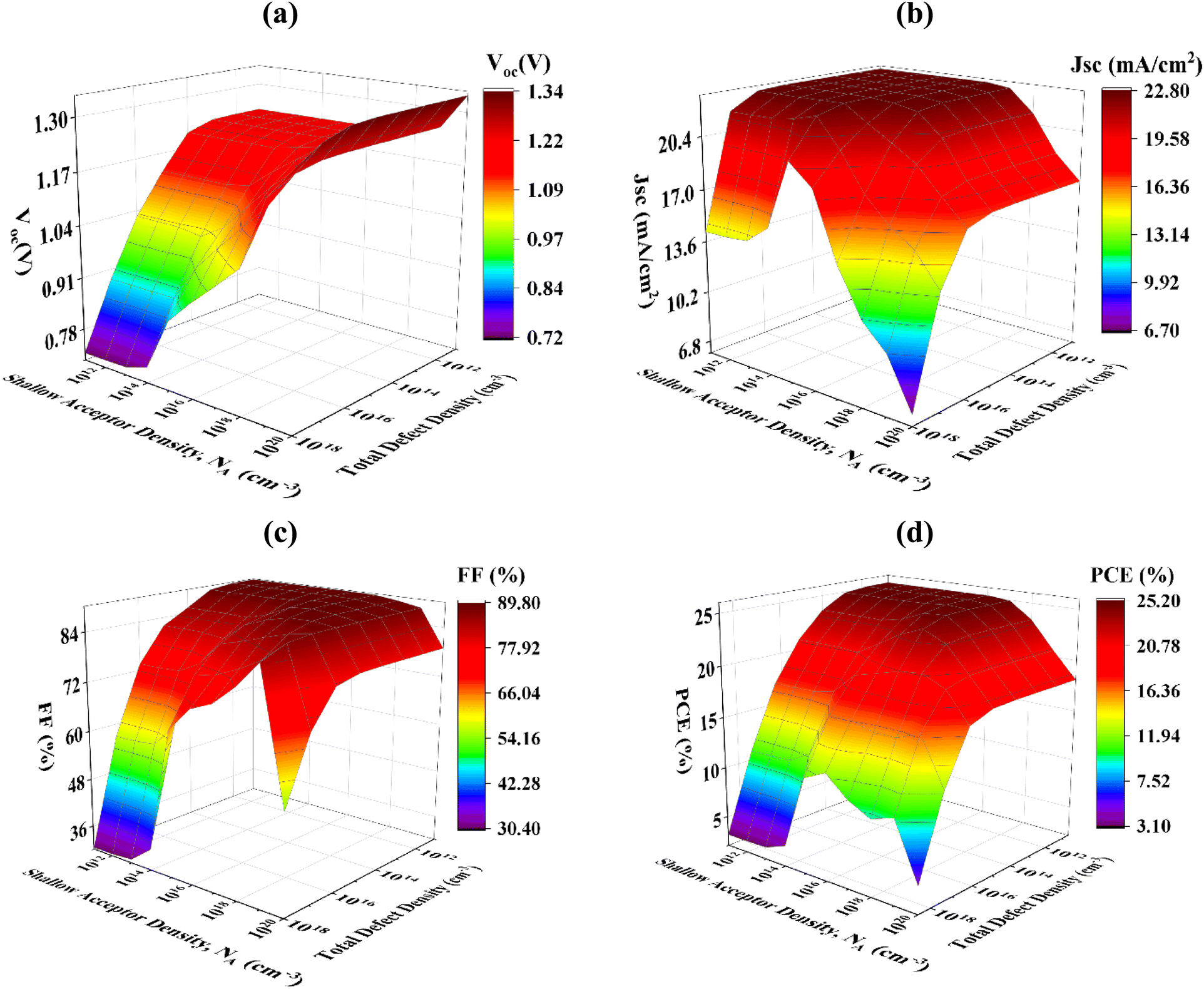
Enhancing solar cell efficiency necessitates a careful equilibrium of multiple parameters, with doping concentrations in the various layers being paramount. An ideal doping density is selected to improve charge carrier extraction, hence directly influencing the device's efficiency. The doping densities are not randomly chosen; they are established through extensive theoretical modeling and simulations. This procedure guarantees that the doping levels are optimized for peak efficiency, as they are crucial in influencing the overall performance of the solar cell. The efficiency of solar cells can be markedly enhanced by optimizing the doping concentrations of various layers, which improves carrier collection and reduces recombination losses, as evidenced by numerous studies.53In this context, fluctuations in defect density (Nt) and acceptor density (NA) markedly influence the performance of PV cells. The effects of these modifications on Cu2O-based HTL solar cells are examined from 1011 to 1018 cm−3 for Nt and from 1011 to 1020 cm−3 for NA in Fig. 5(a–d). In the configuration FTO/ZnO/Sr3PCl3/Cu2O/Ni, variations in Nt and NA result in alterations of the principal performance metrics: PCE, FF, JSC, and VOC, which range from 0.6% to 28.1%, 38.2% to 90.8%, 6.7 mA cm−2 to 22.85 mA cm−2, and 0.78 V to 1.4 V, respectively. Fig. 5(a) indicates that attaining the maximum VOC of 1.4 V necessitates NA > 1019 cm−3 and Nt < 1014 cm−3. Nonetheless, the VOC markedly decreases to 0.78 V when Nt > 1017 cm−3. Fig. 5(b) indicates that the maximum JSC of 22.8 mA cm−2 occurs when Nt < 1014 cm−3 and NA > 1017 cm−3. Fig. 5(c) demonstrates that the FF attains its maximum value of 90.6% when NA is 1019 cm−3 and Nt < 1014 cm−3. Furthermore, FF experiences a significant drop as Nt > 1017 cm−3. Fig. 5(d) illustrates that the maximum PCE over 26% is attained when the NA is 1017 cm−3 and Nt < 1014 cm−3. Introducing a high Nt in the absorber layer elevates carrier recombination, hence reducing cell performance. In the Cu2O HTL structure, optimal parameters for peak efficiency were determined at NA of 1017 cm−3 and Nt of 1014 cm−3. Under these conditions, the solar cell attained a PCE of 26.67%, an FF of 89.9%, a JSC of 22.79 mA cm−2, and a VOC of 1.3 V.
 | ||
| Fig. 5 Impact of Sr3PCl3 absorber acceptor and bulk defect density variations on PV performance ((a) VOC, (b) JSC, (c) FF, and (d) PCE) with Cu2O HTL. | ||
Fig. 6(a–d) illustrate the impact of altering Nt and NA on the efficiency of solar cells employing CBTS as the HTL. Like Cu2O-based cells, performance measures are significantly affected when Nt surpasses 1014 cm−3. In the FTO/ZnO/Sr3PCl3/CBTS/Ni configuration, alterations in Nt and NA lead to fluctuations in PCE, FF, JSC, and VOC, with ranges of 26.8% to 4.3%, 90.6% to 36%, 22.8 mA cm−2 to 6.7 mA cm−2, and 1.37 V to 0.76 V, respectively. Fig. 6(a) indicates that the maximum VOC of 1.37 V is achieved when NA > 1018 cm−3 and Nt < 1014 cm−3. In contrast, the VOC markedly decreases to 0.76 V when Nt exceeds 1017 cm−3. Fig. 6(b) demonstrates that the peak JSC of 22.8 mA cm−2 occurs when Nt < 1014 cm−3 and NA > 1018 cm−3. Furthermore, FF reaches a maximum of 90.6% when NA > 1017 cm−3 and Nt < 1015 cm−3, as illustrated in Fig. 6(c). However, FF significantly decreases to 36% when Nt surpasses 1017 cm−3. Fig. 6(d) demonstrates that the maximum PCE, above 26%, is attained with an NA of 1017 cm−3 and Nt < 1014 cm−3. In these ideal conditions, the solar cell attained a PCE of 26.39%, an FF of 89.84%, a JSC of 22.8 mA cm−2, and a VOC of 1.29 V.
 | ||
| Fig. 6 Impact of Sr3PCl3 absorber acceptor and bulk defect density variations on PV performance ((a) VOC, (b) JSC, (c) FF, and (d) PCE) with CBTS HTL. | ||
Fig. 7(a–d) further investigate the influence of changes in Nt and NA on MoO3-based HTL solar cells. In the FTO/ZnO/Sr3PCl3/MoO3/Ni configuration, performance metrics vary with alterations in Nt and NA, resulting in fluctuations in PCE, FF, JSC, and VOC, which range from 25.2% to 3.1%, 89.8% to 30.4%, 22.8 mA cm−2 to 6.7 mA cm−2, and 1.34 V to 0.72 V, respectively. Fig. 7(a) demonstrates that the maximum VOC of 1.34 V necessitates NA > 1018 cm−3 while Nt < 1014 cm−3. When Nt > 1017 cm−3, VOC decreases to 0.72 V. In Fig. 7(b), a JSC value of 22.8 mA cm−2 is attained when Nt > 1016 cm−3 and NA is below 1017 cm−3. Moreover, the FF attains its maximum at 89.8% when NA < 1017 cm−3 and Nt < 1014 cm−3, as depicted in Fig. 7(c). Fig. 7(d) illustrates that the optimal combination resulting in a PCE over 24% occurs with an NA of 1017 cm−3 and a Nt < 1014 cm−3. Optimal parameters for MoO3-based HTL solar cells, maintaining a fixed NA of 1017 cm−3 and Nt of 1014 cm−3, yield a maximum PCE of 24.86%, an FF of 89.52%, a JSC of 22.55 mA cm−2, and a VOC of 1.23 V.
 | ||
| Fig. 7 Impact of Sr3PCl3 absorber acceptor and bulk defect density variations on PV performance ((a) VOC, (b) JSC, (c) FF, and (d) PCE) with MoO3 HTL. | ||
Fig. 8(a–d) analyze the impact of changes in Nt and NA on solar cells employing CuI as HTL. In the FTO/ZnO/Sr3PCl3/CuI/Ni configuration, the performance metrics exhibit a variation from 22.25% to 2% for PCE, 87.52% to 22.4% for FF, 22.78 mA cm−2 to 6.7 mA cm−2 for JSC, and 1.27 V to 0.67 V for VOC. In Fig. 8(a), the peak VOC of 1.27 V is attained when NA > 1019 cm−3 and Nt < 1016 cm−3, but the VOC diminishes to 0.67 V when Nt > 1017 cm−3. Fig. 8(b) illustrates that a JSC of 22.78 mA cm−2 is attained when Nt < 1016 cm−3 and NA < 1017 cm−3. Fig. 8(c) indicates that FF attains a maximum of 87.52% when NA > 1017 cm−3 and Nt < 1015 cm−3. Fig. 8(d) illustrates that the maximum PCE above 21% is attained when NA is 1017 cm−3 and Nt < 1014 cm−3. The ideal parameters for CuI-based HTL solar cells are NA of 1017 cm−3 and Nt of 1014 cm−3, yielding a maximum PCE of 21.78%, an FF of 87.52%, a JSC of 22.78 mA cm−2, and a VOC of 1.09 V. So, attaining optimal solar cell performance necessitates meticulous adjustment of defects and acceptor densities within each configuration, as evidenced by the discrepancies in these parameters among various HTLs. The results emphasize the necessity of sustaining low defect densities and sufficient acceptor concentrations to optimize solar cell efficiency across diverse material systems.
 | ||
| Fig. 8 Impact of Sr3PCl3 absorber acceptor and bulk defect density variations on PV performance ((a) VOC, (b) JSC, (c) FF, and (d) PCE) with CuI HTL. | ||
3.7 Influence of HTL acceptor density and bulk defect variation on PV efficiency
The efficacy of PV systems is markedly affected by NA of HTL. Doping HTL is a crucial method for optimizing PV performance by improving conductivity between the electrode surface and absorber layer. NA directly influences the attributes of PV structures, including bandgap, carrier concentration, and electrical conductivity. Fig. 9(a) illustrates the impact of altering the NA from 1014 to 1022 cm−3 on PV characteristics in structures incorporating Cu2O, CBTS, MoO3, and CuI HTLs. The performance measurements display the subsequent ranges: PCE rises from 25.93% to 26.67%, 23.17% to 26.67%, 20.38% to 26.48%, and 18.10% to 23.76%; FF ascends from 89.29% to 89.90%, 88.35% to 89.90%, 84.82% to 89.67%, and 78.49% to 87.27%; JSC increases from 22.75 to 22.79 mA cm−2, 21.83 to 22.80 mA cm−2, 20.49 to 22.78 mA cm−2, and remains at 22.78 mA cm2; and VOC enhances from 1.27 to 1.3 V, 1.2 to 1.3 V, 1.17 to 1.29 V, and 1.01 to 1.19 V. Of the analyzed structures, Cu2O HTL exhibits the highest performance, achieving a PCE of roughly 26.67%, JSC of 22.79 mA cm−2, VOC of 1.3 V, and FF of 89.9%. In comparison, CBTS attains a PCE of 26.39%, MoO3 achieves 24.86%, and CuI reaches 21.78%. The results demonstrate that Cu2O has enhanced charge carrier collection and transport capabilities, leading to improved device efficiency. A NA of 1020 cm−3 was chosen for all HTLs to enhance performance and ensure cost-effective production. | ||
| Fig. 9 Influence of changes in (a) acceptor density and (b) defect density with various HTL materials on PV performance. | ||
The Nt in HTLs significantly impacts PV performance by affecting recombination processes and charge carrier dynamics. An elevated Nt can impede charge transport, augment recombination losses, and undermine the structural integrity of the device. Furthermore, non-uniform defect distributions can modify the optical characteristics of the HTL, influencing photon absorption and spatial uniformity in device efficacy.54 To reduce recombination losses and guarantee reliability, it is crucial to maintain low Nt and homogeneity in HTL. Fig. 9(b) illustrates the impact of altering Nt varying from 1012 to 1018 cm−3 on the PV properties for the four-hole transport layers. Notably, despite variations in Nt, the PV measurements stay largely unchanged across all structures. The PCE for Cu2O, CBTS, MoO3, and CuI HTLs are 26.67%, 26.38%, 24.86%, and 21.78%, respectively. Correspondingly, FF persists at 89.90%, 89.83%, 89.52%, and 87.52%, respectively. The JSC exhibits minimal fluctuation, maintaining values of 22.8 mA cm−2, 22.79 mA cm−2, 22.55 mA cm−2, and 22.78 mA cm−2, respectively. Similarly, the VOC remains constant at 1.3 V, 1.28 V, 1.23 V, and 1.09 V, respectively. The findings indicate that Nt below 1015 cm−3 exerts negligible influence on device performance, establishing this as the optimal number for practical applications and further computations.
3.8 Influence of interface defect density on PV efficiency
Interface defects considerably impact on the output characteristics of PV devices, significantly affecting their efficiency and performance stability. Fig. 10 demonstrates the impact of interface defect density (Ntf), ranging from 1010 to 1018 cm−2, on the PV characteristics of Sr3PCl3-based PSCs at the Cu2O/Sr3PCl3, CBTS/Sr3PCl3, MoO3/Sr3PCl3, and CuI/Sr3PCl3 interfaces, while maintaining all other parameters constant. | ||
| Fig. 10 Influence of variations in Ntf at various HTL/Sr3PCl3 layers on PV performance. | ||
At the CuI/Sr3PCl3 interface, performance measurements exhibit considerable degradation with an increase in Ntf. The PCE lowers from 22.59% to 17.10%, the FF diminishes from 85.89% to 82.1%, and the VOC reduces from 1.15 V to 0.93 V. The JSC remains stable at 22.73 mA cm−2 until a Ntf of 1014 cm−2 is reached, after which it starts to decrease. The Cu2O/Sr3PCl3 interface exhibits exceptional stability in PV metrics with rising Ntf up to 1014 cm−2, maintaining PCE, FF, JSC, and VOC values at 26.67%, 89.9%, 22.79 mA cm−2, and 1.3 V, respectively. Exceeding this threshold, the parameters start to diminish, signifying the effect of accelerated recombination at elevated defect densities.
At the CBTS/Sr3PCl3 interface, a marginal decrease in VOC is seen, diminishing from 1.3 V to 1.16 V when Ntf increases to 1013 cm−2. The PCE and JSC exhibit a more pronounced decrease, falling from 26.6% to 19.78% and from 22.8 to 19.58 mA cm−2, respectively. The FF remains stable at 89.83% up to 1013 cm−2 before exhibiting slight reductions.
The MoO3/Sr3PCl3 interface exhibits heightened sensitivity to Ntf. A decline in performance is noted beginning at 1010 cm−2, with measurements stabilizing at Ntf of 1014 cm−2. The PCE, FF, JSC, and VOC stabilized at 19.76%, 86.93%, 19.58 mA cm−2, and 1.16 V, respectively. Interface defects are directly associated with elevated series resistance, which negatively affects performance.55 Nonetheless, JSC exhibits minimal impact across all surfaces because of its reduced sensitivity to variations in resistance. The noted reductions in PCE, FF, and VOC are ascribed to expedited carrier recombination at elevated Ntf, which reduces charge-collecting efficiency and amplifies energy losses. Interface defects at the Cu2O/Sr3PCl3, CBTS/Sr3PCl3, MoO3/Sr3PCl3, and CuI/Sr3PCl3 layers constitute a significant determinant affecting the efficacy and dependability of PV systems.55,56 To enhance PV efficiency, it is essential to minimize interface defects, maintain uniformity at the interfaces, and diminish recombination losses attributed to defect density.
3.9 Examination of generation-recombination rates and carrier densities
The generation and recombination rates of charge carriers are essential factors in assessing the efficiency of PV systems. Fig. 11(a and b) illustrates the carrier recombination and generation rates for all four structures at various positions. Carrier generation transpires when an electron shifts from the valence band (VB) to the conduction band (CB), resulting in the formation of electron–hole pairs.57 This mechanism releases free carriers, improving the overall charge production in PSCs. Structure III shows the lowest generation rate at 0.05 μm, while structures I, II, and IV display peak production rates at 0.1 μm. This fluctuation results from localized disparities in photon absorption, influenced by material characteristics and structural design. Eqn (4) delineates the generation rate G (λ, x), computed utilizing the SCAPS-1D model and the photon flow.| G (λ, x) = α (λ, x)·Nphoton (λ, x) | (4) |
 | ||
| Fig. 11 Impact of HTL variations on (a) total generation rates, (b) total recombination rates, (c) electron concentration, and (d) hole concentration. | ||
Recombination transpires when electrons and holes merge, resulting in a depletion of charge carriers. In PSCs, recombination is influenced by the density and lifespan of charge carriers, together with defects present in each layer. During recombination, CB electrons transition to the VB by overcoming an energy barrier and combining with holes. The corresponding energy levels govern the kinetics of this process, rendering it a vital factor in PSC performance. Fig. 11(b) illustrates that structure III exhibits the lowest recombination rate at 0.04 μm, while structures I, II, and IV demonstrate elevated recombination rates at 0.1 μm.
Fig. 11(c and d) analyze the impact of altering the thickness of the Sr3PCl3 on electron and hole concentrations inside the four device configurations. Variations in Sr3PCl3 layer thickness modify DOS in the VBs, influencing the distribution and quantity of holes in the Sr3PCl3 layer. Holes are significantly more prevalent than electrons, a fact ascribed to the material characteristics of Sr3PCl3 and the selection of HTLs.58,59 The incorporation of HTLs such as Cu2O, CBTS, MoO3, and CuI with Sr3PCl3 perovskite markedly diminishes electron–hole recombination and enhances carrier production. This analysis indicates that reducing recombination and optimizing carrier generation rates can enhance the efficiency of PSCs. The results underscore the significance of absorber thickness, photon absorption, and HTL compatibility in enhancing the overall efficacy of PSCs.
3.10 Influence of temperature on PV efficiency
The operational temperature of a solar cell frequently surpasses ambient temperature, considerably affecting its PV efficiency. To examine this effect, the temperature was altered from 275 K to 500 K, and its influence on PV parameters is illustrated in Fig. 12. Temperature variations influence critical parameters, including PCE, FF, and VOC, although the JSC remains mostly unchanged. | ||
| Fig. 12 Temperature-dependent analysis of PV parameters under diverse HTL configurations. | ||
In the basic configuration utilizing Cu2O HTL, the PCE diminishes from 27.68% at 275 K to 18.36% at 500 K. Correspondingly, for CBTS HTL, the PCE decreases from 27.17% to 18.36%; for MoO3 HTL, it declines from 24.32% to 18.31%; and for CuI HTL, it falls from 22.1% to 14.45%. The decline in PCE across all structures is due to a variety of variables, including lower shunt resistance and increased charge recombination rates at elevated temperatures.
A significant observation is the temperature-dependent reduction in VOC. As temperature increases, the reverse saturation current density (J0) escalates, reducing VOC. This relationship is defined by eqn (5).
 | (5) |
 , KB, A, T, and q).
The equation illustrates that the rise in J0 with temperature adversely affects VOC. Simulations indicate that JSC is predominantly impervious to temperature fluctuations. Nevertheless, FF and PCE exhibit a significant decrease with rising temperature. The decrease in FF and PCE can be attributed to the decline in charge recombination resistance and the enhancement in the rate of electron–hole recombination between the valence and conduction bands.60 Elevated temperatures accelerate charge recombination processes, consequently decreasing total charge-collecting efficiency and impairing solar cell performance.
Furthermore, in specific PSC arrangements, elevated temperatures accelerate the recombination of electrons and holes, hence exacerbating the increase in J0 and the resultant decrease in VOC and PCE.61,62 These findings underscore the paramount significance of temperature regulation in solar cell design. By alleviating the detrimental impacts of temperature on PV characteristics, either material optimization or the integration of thermal management systems, the efficacy, and durability of PSCs can be substantially improved.
3.11 Optimized J–V and QE properties
A thicker Sr3PCl3 absorber layer often improves photocurrent by augmenting light absorption, leading to an elevated JSC. Nonetheless, this benefit has trade-offs, as increased thickness may result in elevated recombination losses. These losses may diminish the FF and VOC, thus impairing the overall PCE. Determining an ideal absorber layer thickness is essential, necessitating meticulous attention to structural design, processing methods, and doping concentrations. Some research indicates that smaller absorber layers may surpass bulkier layers by minimizing the recombination process.63,64 The thickness of the absorber layer greatly affects its QE. Thicker Sr3PCl3 layers absorb a higher quantity of photons, resulting in improved QE at longer wavelengths (Fig. 13). | ||
| Fig. 13 J–V and QE responses for (a and b) structure I, (c and d) structure II, (e and f) structure III, and (g and h) structure IV. | ||
Fig. 13(a, c, e and g) and (b, d, f and h) depict the J–V and QE characteristics of solar cells utilizing Cu2O, CBTS, MoO3, and CuI HTLs, respectively. The optimized configurations attained peak PCE of 26.67%, 26.38%, 24.86%, and 21.78%, with associated VOC of 1.30 V, 1.28 V, 1.23 V, and 1.09 V. FF were documented as 89.90%, 89.83%, 89.52%, and 87.52%, whereas JSC values were 22.79 mA cm−2, 22.79 mA cm−2, 22.55 mA cm−2, and 22.78 mA cm−2 for Cu2O, CBTS, MoO3, and CuI, respectively. The examination of J–V curves indicates a steady decline in current density with rising voltage, as depicted in Fig. 13 (a, c, e and g). These trends illustrate the characteristic behavior of PV systems, wherein increasing voltage diminishes the impetus for charge extraction. The QE profiles encompass a wavelength range of 300 nm to 850 nm, commencing at about 100% efficiency and progressively diminishing to 0% as the wavelength nears 750 nm. This reduction is uniform across all configurations, as illustrated in Fig. 13(b, d, f and h). The correlation of J–V and QE characteristics highlights the relationship between absorber layer thickness and device efficacy. By meticulously adjusting the Sr3PCl3 layer thickness and refining the interface with HTLs such as Cu2O, CBTS, MoO3, and CuI, high-efficiency solar cells can be attained. This optimization reduces recombination losses and improves photon absorption, facilitating enhanced charge carrier generation and extraction.
3.12 Bifacial PSCs utilizing the FTO/ZnO/Sr3PCl3/(Cu2O/CBTS/MoO3/CuI)/Ni configurations
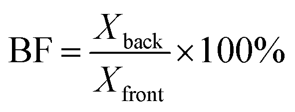
The research examines bifacial PSCs utilizing the distinctive material composition FTO/ZnO/Sr3PCl3/(Cu2O/CBTS/MoO3/CuI)/Ni, employing a bifacial structure to improve energy-harvesting efficiency. Bifacial PSCs, in contrast to traditional mono-facial PSCs that absorb sunlight simply from one side, are engineered to capture light from both the front and back sides, hence enhancing energy yield per unit area.65 This method diminishes the supplementary expenses and complexity usually linked to the production of bifacial cells, rendering it a viable choice for scalable solar technology. This work presents a solution that simplifies traditional bifacial PSC production, which often necessitates substantial optimization for effective back-side lighting, while yet achieving high conversion efficiency.Two independent simulations were performed to assess performance under different illumination conditions, examining the impact of light entering from both the front and rear sides of the PSC. This dual study provided essential information into the device's PV performance. Essential measures, such as bifacial factors (BF) and bifacial gain (BG), were computed to assess comparative efficiency and supplementary energy contributions from rear-side lighting. The BF assesses the comparative performance of each side and is computed using eqn (6).
 | (6) |
BG denotes the supplementary efficiency contribution from back-side lighting and is described by eqn (7).
 | (7) |
Bifacial efficiency (ηbi) is determined using the formula in eqn (8).
| ηbi = ηfront + ηback (at 20% of 1 sun) | (8) |
Fig. 14(a–c) displays the current density–voltage (J–V) curves for four unique structures (I, II, III, and IV) under optimal front and rear illumination condition and the bifacial performance. Performance with back-side illumination (1 sun intensity) was found to be inferior to that with front-side illumination, indicating that absorption losses on the rear surface diminish overall efficiency. Table 3 summarizes the essential PV parameters for both illumination conditions throughout the four device configurations. The BF values for VOC, JSC, FF, and PCE for structures I–IV under back-side light are detailed below:
 | ||
| Fig. 14 Investigation of J–V curves for the FTO/ZnO/Sr3PCl3/(Cu2O/CBTS/MoO3/CuI)/Ni device structure with (a) both front and (b) back illumination under 1 sun conditions and (c) a bifacial configuration. | ||
| Structure I–IV | Illumination condition | VOC (V) | JSC (mA cm−2) | FF (%) | PCE (%) |
|---|---|---|---|---|---|
| FTO/ZnO/Sr3PCl3/Cu2O/Ni | Front side | 1.3 | 22.79 | 89.9 | 26.67 |
| Back side | 1.29 | 19.95 | 89.86 | 23.26 | |
| FTO/ZnO/Sr3PCl3/CBTS/Ni | Front side | 1.29 | 22.8 | 89.84 | 26.39 |
| Back side | 1.28 | 19.69 | 89.78 | 22.72 | |
| FTO/ZnO/Sr3PCl3/MoO3/Ni | Front side | 1.23 | 22.55 | 89.52 | 24.86 |
| Back side | 1.2 | 19.43 | 89.44 | 21.37 | |
| FTO/ZnO/Sr3PCl3/CuI/Ni | Front side | 1.09 | 22.78 | 87.52 | 21.78 |
| Back side | 1.087 | 18.8 | 87.12 | 17.88 |
• VOC: 99.23%, 99.61%, 99.67%, and 99.63%.
• JSC: 87.53%, 86.39%, 86.16%, and 87.00%.
• FF: 99.96%, 99.93%, 99.91%, and 99.54%.
•PCE: 87.21%, 86.09%, 85.96%, and 82.09%.
The results demonstrate that VOC and FF are essentially unchanged by back-side illumination, although JSC and PCE show slightly reduced BF values, underscoring the occurrence of back-surface absorption losses.66
The BG and ηbi were computed for structures I–IV using eqn (7) and (8), yielding values of 16.74%, 16.53%, 16.14%, and 15.92%, and 31.07%, 30.53%, 29.21%, and 24.46% respectively. These findings align with earlier reports,67,68 illustrating the capacity of bifacial solar cells to markedly increase energy production relative to mono-facial counterparts. The durable material architecture and significant energy-harvesting capability of bifacial PV solar cells highlight its benefits in contemporary solar technology. An in-depth examination of BF and BG characteristics underscores the capacity of these devices to sustain performance throughout varying lighting conditions. Bifacial solar cells provide a practical and economical solution for substantially enhancing solar energy conversion efficiency by efficiently mitigating back-side absorption losses and improving their structure.
3.13 Improved device performance compared to prior research
Compared to earlier research, the present device is a significant improvement. In recent years, the efficacy of A3BX3-based PSCs has shown consistent enhancements.24,27,69 This work presents a unique solar cell configuration comprising FTO/ZnO/Sr3PCl3/Cu2O/Ni, which has attained a remarkable efficiency of 26.67%. This achievement is primarily ascribed to the synergistic integration of Cu2O, serving as HTL, and ZnO, operating as ETL. This device demonstrated a VOC of 1.3 V, a JSC of 22.79 mA cm−2, and an FF of 89.9%. Table 4 presents a comparison of the performance parameters of the latest configuration with those from prior research, highlighting the substantial enhancement in efficiency.| Device structure | Type work | VOC (V) | JSC (mA cm−2) | FF (%) | PCE (%) | Ref. |
|---|---|---|---|---|---|---|
| FTO/SnS2/Sr3NCl3 | T | 1.24 | 16.79 | 86.44 | 18.11 | 27 |
| Al/FTO/SnS2/Ca3SbI3/MoO3/Au | T | 1.16 | 19.07 | 87.79 | 19.47 | 69 |
| ITO/SnO2/CH3NH3SnI3/CuSCN | T | 0.92 | 34.38 | 74.46 | 23.57 | 70 |
| Zn/FASnI3/CuSCN | T | 1.08 | 28.12 | 84.96 | 25.94 | 71 |
| ITO/TiO2/CsSnBr3/Spiro-OMeTAD/Au | E | 0.85 | 21.23 | 58 | 10.46 | 72 |
| ITO/TiO2/MASnI3/Spiro-OMeTAD/Au | E | 0.88 | 16.8 | 42 | 6.4 | 73 |
| CsPbI3/Cs0.25FA0.75PbI3 | E | 1.20 | 18.91 | 76.00 | 17.39 | 74 |
| CsPbI3/FAPbI3 | E | 1.22 | 17.26 | 74.00 | 15.6 | 75 |
| FTO/ZnO/Sr3PCl3/Cu2O/Ni | T | 1.30 | 22.79 | 89.90 | 26.67 | This work |
| FTO/ZnO/Sr3PCl3/CBTS/Ni | T | 1.28 | 22.79 | 89.83 | 26.38 | This work |
| FTO/ZnO/Sr3PCl3/MoO3/Ni | T | 1.23 | 22.55 | 89.52 | 24.86 | This work |
| FTO/ZnO/Sr3PCl3/CuI/Ni | T | 1.09 | 22.78 | 87.52 | 21.78 | This work |
4 Conclusion
This study numerically assessed the promising optoelectronic characteristics of Sr3PCl3-based PSCs by SCAPS-1D simulations and DFT calculations. The work concentrated on an innovative heterostructure design consisting of FTO/ZnO/Sr3PCl3/(Cu2O/CBTS/MoO3/CuI)/Ni and evaluated its efficacy in photovoltaic applications. The essential device parameters, encompassing the characteristics of the Sr3PCl3 absorber and the functions of several HTLs, were methodically examined. The ideal configuration comprises a Sr3PCl3 layer with a thickness of 1000 nm and NA of 1017 cm−3, along with HTL and ETL layers having thicknesses of 100 nm and 50 nm, respectively. Among the examined HTLs, Cu2O exhibited the highest PCE of 26.67%, with a VOC of 1.3 V, a JSC of 22.79 mA cm−2, and an FF of 89.9%. In contrast, the CBTS, MoO3, and CuI HTLs attained PCE of 26.39%, 24.86%, and 21.78%, respectively, with corresponding VOC values of 1.29 V, 1.23 V, and 1.09 V, JSC values of 22.8 mA cm−2, 22.55 mA cm−2, and 22.78 mA cm−2, and FF of 89.84%, 89.52%, and 87.52%. Additionally, the proposed four PSC configurations for bifacial Sr3PCl3 PSCs indicate that performance under front illumination was slightly higher than that under back illumination. The BF of the PCE was recorded at 87.21%, 86.09%, 85.96%, and 82.09% for structures I, I, II, III, and IV, respectively, while the BG and ηbi for these structures was documented as 16.74%, 16.53%, 16.14%, and 15.92% and 31.07%, 30.53%, 29.21%, and 24.46%, indicating consistent efficiency patterns throughout the configurations. The results underscore the capability of the suggested FTO/ZnO/Sr3PCl3/Cu2O/Ni heterojunction configuration to produce high-efficiency in both mono-facial and bifacial solar cells. The exhibited synergy of superior photovoltaic efficiency and economical material utilization highlights the potential of Sr3PCl3 as a formidable contender for the progression of solar cell technology in the energy domain.Ethical statement
All authors state that the manuscript does not involve humans, human data or tissue, or animals.Data availability
The authors can provide supporting data for this study upon request.Author contributions
Asadul Islam Shimul: simulation, resources, formal analysis, data curation, conceptualization, methodology, original manuscript writing, data acquisition, and validation. Avijit Ghosh: supervision, manuscript editing, revision and validation. Swarna Rani Sarker: simulation, data acquisition, and validation. Huriyyah A. Alturaifi: manuscript editing, revision and validation.Conflicts of interest
The authors state that they have no knowledge of competing financial interests or personal relationships that could have influenced this paper.Acknowledgements
The authors extend their appreciation to the Deanship of Research and Graduate Studies at King Khalid University for funding this work under grant number RGP2/246/45.References
- A. Q. Al-Shetwi, I. Z. Abidin, K. A. Mahafzah and M. A. Hannan, J. Clean. Prod., 2024, 478, 143942 CrossRef.
- S. Aftab, S. Hussain, F. Kabir, M. Aslam, A. H. Rajpar and A. G. Al-Sehemi, Nano Energy, 2024, 120, 109112 CrossRef CAS.
- F.-T. Zahra, M. M. Hasan, M. B. Hossen and M. R. Islam, Heliyon, 2024, 10, e33096 CrossRef CAS PubMed.
- N. K. Elangovan, R. Kannadasan, B. B. Beenarani, M. H. Alsharif, M.-K. Kim and Z. Hasan Inamul, Energy Rep., 2024, 11, 1171–1190 CrossRef.
- I. López-Fernández, D. Valli, C. Wang, S. Samanta, T. Okamoto, Y. Huang, K. Sun, Y. Liu, V. S. Chirvony, A. Patra, J. Zito, L. De Trizio, D. Gaur, H. Sun, Z. Xia, X. Li, H. Zeng, I. Mora-Seró, N. Pradhan, J. P. Martínez-Pastor, P. Müller-Buschbaum, V. Biju, T. Debnath, M. Saliba, E. Debroye, R. L. Z. Hoye, I. Infante, L. Manna and L. Polavarapu, Adv. Funct. Mater., 2024, 34, 2307896 CrossRef.
- V. Deswal, S. Kaushik, R. Kundara and S. Baghel, Mater. Sci. Eng. B, 2024, 299, 117041 CrossRef CAS.
- M. S. Hossen, K. Alam, M. A. Mostakim, U. Mahmud, M. A. Imran and A. A. Fathah, Int. J. Sci. Res. Manag., 2022, 10, 946–962 Search PubMed.
- A. A. Hassan, M. S. Islam Ria, A. Ghosh, H. A. Alrafai, A. Al Baki, S. Khalaf Alla Abdelrahim, J. Y. Al-Humaidi, R. Islam Chowdhury Robin, M. M. Rahman and M. Maniruzzaman, Mater. Sci. Eng. B, 2024, 308, 117559 CrossRef CAS.
- M. Rahaman, M. Hasan, R. M. Moinuddin and M. N. Islam, AIP Adv., 2024, 14, 095019 CrossRef CAS.
- S. Joifullah, M. A. Hossain, M. Al Yeamin, M. M. Haque, R. K. Pingak, N. F. A. Mohammad, M. S. Abu-Jafar, A. A. Mousa and A. Hosen, Opt. Quant. Electron., 2024, 56, 1463 CrossRef CAS.
- J. Lü, X. Huo, W. Liu, W. Sun, S. Ji, T. You, K. Wang, W. Lü and S. Wang, Mater. Today Energy, 2024, 44, 101628 CrossRef.
- S. Rajabzade, K. Abdizadeh, F. A. Mahyari, F. Tajabadi, M. Heidariramsheh, M. Forouzandeh and N. Taghavinia, J. Power Sources, 2025, 630, 236134 CrossRef CAS.
- T. Zhang, M. I. Dar, G. Li, F. Xu, N. Guo, M. Grätzel and Y. Zhao, Sci. Adv., 2017, 3, e1700841 CrossRef PubMed.
- B. Li, Y. Zhang, L. Fu, T. Yu, S. Zhou, L. Zhang and L. Yin, Nat. Commun., 2018, 9, 1076 CrossRef PubMed.
- H. Zhu, S. Teale, M. N. Lintangpradipto, S. Mahesh, B. Chen, M. D. McGehee, E. H. Sargent and O. M. Bakr, Nat. Rev. Mater., 2023, 8, 569–586 CrossRef.
- G. A. Nowsherwan, Q. Ali, N. Nowsherwan, U. F. Ali and S. S. Hussain, Multiscale Multidiscip. Model. Exp. Des., 2025, 8, 10 CrossRef.
- M. H. Ishraq, M. R. Kabir, M. Tarekuzzaman, M. F. Rahman, M. Rasheduzzaman and M. Z. Hasan, Adv. Theory Simul., 2024, 7, 2400360 CrossRef CAS.
- W. Wang, X. Li, P. Huang, L. Yang, L. Gao, Y. Jiang, J. Hu, Y. Gao, Y. Che, J. Deng, J. Zhang and W. Tang, Adv. Mater., 2024, 2407349 CrossRef CAS PubMed.
- S. Bhattarai, Mater. Chem. Phys., 2024, 318, 129269 CrossRef CAS.
- H. Tang, Y. Bai, H. Zhao, X. Qin, Z. Hu, C. Zhou, F. Huang and Y. Cao, Adv. Mater., 2024, 36, 2212236 CrossRef CAS PubMed.
- J. Chen, Z. Wu, S. Chen, W. Zhao, Y. Zhang, W. Ye, R. Yang, L. Gong, Z. Peng and J. Chen, Mater. Sci. Semicond. Process., 2024, 174, 108186 CrossRef CAS.
- C. Yang, W. Hu, J. Liu, C. Han, Q. Gao, A. Mei, Y. Zhou, F. Guo and H. Han, Light Sci. Appl., 2024, 13, 227 Search PubMed.
- A. I. Shimul, A. T. M. S. Islam, A. Ghosh, M. M. Hossain, S. A. Dipa and R. J. Ramalingam, Comput. Mater. Sci., 2025, 250, 113701 CrossRef CAS.
- A. Ghosh, A. Bakkar, Momina, N. Asmat, F. Ahmed, M. F. I. Buian, M. Sajid, J. R. Rajabathar, A. M. Karami, A. Nandi and M. A. Islam, J. Phys. Chem. Solids, 2024, 190, 112029 CrossRef CAS.
- M. F. Rahman, M. Rahman, M. F. Hossain, B. Islam, S. R. Al Ahmed and A. Irfan, Adv. Photonics Res., 2024, 2400148 CrossRef.
- K. K. Mishra, S. Chahar and R. Sharma, Phys. Lett. A, 2024, 523, 129817 Search PubMed.
- M. A. Rahman, M. F. Rahman, L. Marasamy, M. Harun-Or-Rashid, A. Ghosh, A. R. Chaudhry and A. Irfan, Energy Fuels, 2024, 38, 8199–8217 Search PubMed.
- A. I. Shimul, A. Ghosh, M. A. Bappy, M. B. Islam, S. O. Aljazzar, J. Y. Al-Humaidi and Y. E. Mukhrish, Opt. Commun., 2025, 579, 131558 CrossRef CAS.
- D. B. Khadka, Y. Shirai, M. Yanagida and K. Miyano, ACS Appl. Mater. Interfaces, 2019, 11, 7055–7065 Search PubMed.
- H. Wang, Z. Qin, X. Li, C. Zhao and C. Liang, Energy Environ. Eng., 2024, 7, e12666 CAS.
- G. Kresse and J. Hafner, J. Phys. Condens. Matter, 1994, 6, 8245–8257 CrossRef CAS.
- M. Rizwan, A. Ali, Z. Usman, N. R. Khalid, H. B. Jin and C. B. Cao, Phys. B Condens. Matter, 2019, 552, 52–57 CrossRef CAS.
- D. R. Hamann, M. Schlüter and C. Chiang, Phys. Rev. Lett., 1979, 43, 1494–1497 CrossRef CAS.
- J. P. Perdew, K. Burke and M. Ernzerhof, Phys. Rev. Lett., 1996, 77, 3865–3868 Search PubMed.
- J. D. Head and M. C. Zerner, Chem. Phys. Lett., 1985, 122, 264–270 CrossRef CAS.
- M. Burgelman, P. Nollet and S. Degrave, Thin Solid Films, 2000, 361–362, 527–532 CrossRef CAS.
- M. Mostefaoui, H. Mazari, S. Khelifi, A. Bouraiou and R. Dabou, Energy Procedia, 2015, 74, 736–744 CrossRef CAS.
- M. Roknuzzaman, K. Ostrikov, H. Wang, A. Du and T. Tesfamichael, Sci. Rep., 2017, 7, 14025 CrossRef PubMed.
- T.-Y. Tang and Y.-L. Tang, Chem. Phys., 2023, 570, 111897 Search PubMed.
- M. Husain, N. Rahman, N. Sfina, N. H. Al-Shaalan, S. Alharthi, S. A. Alharthy, M. A. Amin, V. Tirth, R. Khan, M. Sohail, A. Azzouz-Rached, S. A. Khattak and M. Y. Khan, Opt. Quant. Electron., 2023, 55, 920 CrossRef CAS.
- M. A. Rahman, M. F. Rahman, L. Marasamy, M. Harun-Or-Rashid, A. Ghosh, A. R. Chaudhry and A. Irfan, Energy Fuels, 2024, 38, 8199–8217 Search PubMed.
- A. I. Shimul, M. M. Haque, A. Ghosh, M. A. U. Sunny, S. O. Aljazzar, J. Y. Al-Humaidi and Y. E. Mukhrish, J. Inorg. Organomet. Polym. Mater., 2025 DOI:10.1007/s10904-025-03629-3.
- P. L. Polavarapu, J. Phys. Chem. A, 2005, 109, 7013–7023 CrossRef CAS PubMed.
- M. F. Rahman, M. H. Rahman, M. R. Islam, M. K. Hossain, A. Ghosh, M. S. Islam, M. M. Islam, M. Harun-Or-Rashid, H. Albalawi and Q. Mahmood, J. Mater. Sci., 2023, 58, 13100–13117 CrossRef CAS.
- W. Zulhafizhazuan, K. Sobayel, S. Shafian, S. Sepeai and M. A. Ibrahim, Interactions, 2025, 246, 29 CrossRef CAS.
- K. I. Ferdous Utsho, S. M. G. Mostafa, M. Tarekuzzaman, M. S. M. Al-Saleem, N. I. Nahid, J. Y. Al-Humaidi, M. Rasheduzzaman, M. M. Rahman and M. Z. Hasan, RSC Adv., 2025, 15, 2184–2204 RSC.
- A. I. Shimul, A. T. M. S. Islam, A. Ghosh, M. M. Hossain, S. A. Dipa and R. J. Ramalingam, Comput. Mater. Sci., 2025, 250, 113701 Search PubMed.
- M. K. Hossain, M. K. A. Mohammed, R. Pandey, A. A. Arnab, M. H. K. Rubel, K. M. Hossain, M. H. Ali, M. F. Rahman, H. Bencherif, J. Madan, M. R. Islam, D. P. Samajdar and S. Bhattarai, Energy Fuels, 2023, 37, 6078–6098 Search PubMed.
- K. T. Arockiya Dass, M. K. Hossain and L. Marasamy, Sci. Rep., 2024, 14, 1473 CrossRef CAS PubMed.
- M. Aliaghayee, J. Electron. Mater., 2023, 52, 2475–2491 CrossRef CAS.
- S. Rabhi, K. Sekar, K. Kalna, Y. I. Bouderbala, N. Bouri, N. Oueldna, N. Belbachir, K. Dadda, M. S. Aida and N. Attaf, Opt. Quant. Electron., 2024, 56, 1372 CrossRef CAS.
- S. Yasin, T. Al Zoubi and M. Moustafa, Optik, 2021, 229, 166258 Search PubMed.
- E. L. Meyer, S. A. Mvokwe, O. O. Oyedeji, N. Rono and M. A. Agoro, Materials, 2025, 18, 186 CrossRef CAS PubMed.
- S. Datta, M. M. Hossain, S. Nuzhat, A. Debnath and H. Huq, in 2022 IEEE Green Technologies Conference (GreenTech), IEEE, Houston, TX, USA, 2022, pp. 80–85 Search PubMed.
- M. F. Rahman, M. M. Ahmad, T. A. Chowdhury and S. Singha, Sol. Energy, 2022, 240, 1–12 CrossRef CAS.
- M. M. Khatun, A. Sunny and S. R. A. Ahmed, Sol. Energy, 2021, 224, 956–965 CrossRef CAS.
- M. S. Reza, A. Ghosh, S. N. Wornob, M. S. Reza, A. K. Azad, M. M. Hossain, N. S. Awwad and H. A. Ibrahium, J. Phys. Chem. Solids, 2024, 194, 112250 CrossRef CAS.
- A. C. Nkele, I. S. Ike, S. Ezugwu, M. Maaza and F. I. Ezema, Int. J. Energy Res., 2021, 45, 1496–1516 CrossRef CAS.
- S. Ijaz, E. Raza, Z. Ahmad, M. Zubair, M. Q. Mehmood, H. Mehmood, Y. Massoud and M. M. Rehman, Sol. Energy, 2023, 250, 108–118 CrossRef CAS.
- M. K. Hossain, M. S. Uddin, G. F. I. Toki, M. K. A. Mohammed, R. Pandey, J. Madan, M. F. Rahman, M. R. Islam, S. Bhattarai, H. Bencherif, D. P. Samajdar, M. Amami and D. K. Dwivedi, RSC Adv., 2023, 13, 23514–23537 RSC.
- J. Borah, S. Baruah and S. Rajasekaran, J. Electron. Mater., 2025, 54, 944–961 CrossRef CAS.
- N. Jahan, A. Ghosh, F. Ahmed, M. F. I. Buian, M. Y. Ali, A. A. Miazee, M. Sajid, A. Nandi, M. M. H. Emon, M. K. Rahman and M. A. Azad, J. Opt., 2024 DOI:10.1007/s12596-024-01800-6.
- M. Shamim Reza, A. Ghosh, A. Kalam Azad, M. Selim Reza, M. Mahfuz Hossain, A. Ahammad Miazee, N. S. Awwad, M. Saiful Islam and H. A. Ibrahium, Mater. Sci. Eng. B, 2024, 309, 117656 CrossRef CAS.
- M. A. Rahman, M. F. Rahman, L. Marasamy, M. Harun-Or-Rashid, A. Ghosh, A. R. Chaudhry and A. Irfan, Energy Fuels, 2024, 38, 8199–8217 CrossRef CAS.
- G. G. Untila, T. N. Kost, A. B. Chebotareva, M. B. Zaks, A. M. Sitnikov, O. I. Solodukha and M. Z. Shvarts, Photovolt.: Res. Appl., 2015, 23, 600–610 CrossRef CAS.
- X. Sun, M. R. Khan, C. Deline and M. A. Alam, Appl. Energy, 2018, 212, 1601–1610 CrossRef.
- M. Atowar Rahman, Heliyon, 2022, 8, e09800 CrossRef CAS PubMed.
- A. B. Phillips, K. K. Subedi, G. K. Liyanage, F. K. Alfadhili, R. J. Ellingson and M. J. Heben, ACS Appl. Energy Mater., 2020, 3, 6072–6078 CrossRef CAS.
- M. S. Reza, A. Ghosh, S. N. Wornob, M. S. Reza, A. K. Azad, M. M. Hossain, N. S. Awwad and H. A. Ibrahium, J. Phys. Chem. Solids, 2024, 194, 112250 CrossRef CAS.
- M. S. Hanif, I. Qasim, M. I. Malik, M. F. Nasir, O. Ahmad and A. Rashid, Heliyon, 2024, 10, e25703 CrossRef CAS PubMed.
- S. Rabhi, K. Sekar, K. Kalna, Y. I. Bouderbala, N. Bouri, N. Oueldna, N. Belbachir, K. Dadda, M. S. Aida and N. Attaf, Opt. Quant. Electron., 2024, 56, 1372 CrossRef CAS.
- L.-J. Chen, C.-R. Lee, Y.-J. Chuang, Z.-H. Wu and C. Chen, J. Phys. Chem. Lett., 2016, 7, 5028–5035 CrossRef CAS PubMed.
- N. K. Noel, S. D. Stranks, A. Abate, C. Wehrenfennig, S. Guarnera, A.-A. Haghighirad, A. Sadhanala, G. E. Eperon, S. K. Pathak, M. B. Johnston, A. Petrozza, L. M. Herz and H. J. Snaith, Energy Environ. Sci., 2014, 7, 3061–3068 RSC.
- Q. Zhao, A. Hazarika, X. Chen, S. P. Harvey, B. W. Larson, G. R. Teeter, J. Liu, T. Song, C. Xiao, L. Shaw, M. Zhang, G. Li, M. C. Beard and J. M. Luther, Nat. Commun., 2019, 10, 2842 CrossRef PubMed.
- F. Li, S. Zhou, J. Yuan, C. Qin, Y. Yang, J. Shi, X. Ling, Y. Li and W. Ma, ACS Energy Lett., 2019, 4, 2571–2578 CrossRef CAS.
| This journal is © The Royal Society of Chemistry 2025 |