
 Open Access Article
 This Open Access Article is licensed under a Creative Commons Attribution-Non Commercial 3.0 Unported Licence
Potassium iodide-doped cesium tin chloride/copper oxide perovskite for light photodetection and energy conversion
Amira H. Ali *a,
Ashour M. Ahmedb,
Safaa M. Abassc,
Ahmed A. Abdel-Khaliekc,
Mohamed Shaband,
Mohannad Al-Hmoudb,
S. Abd El Khalikc and
Mohamed Rabiaa
*a,
Ashour M. Ahmedb,
Safaa M. Abassc,
Ahmed A. Abdel-Khaliekc,
Mohamed Shaband,
Mohannad Al-Hmoudb,
S. Abd El Khalikc and
Mohamed Rabiaa
aNanomaterials Science Research Laboratory, Chemistry Department, Faculty of Science, Beni-Suef University, Beni-Suef, Egypt. E-mail: ah1173@fayoum.edu.eg
bPhysics Department, College of Science, Imam Mohammad Ibn Saud Islamic University (IMSIU), Riyadh 11623, Saudi Arabia
cChemistry Department, Faculty of Science, Beni-Suef University, Beni-Suef, Egypt
dPhysics Department, Faculty of Science, Islamic University of Madinah, Madinah, Saudi Arabia
First published on 8th April 2025
Abstract
Perovskite materials have emerged as up-and-coming candidates for optoelectronic devices. This study developed a photodetector by depositing a halide double perovskite material, KI-doped Cs2SnCl6 (KI:CTC), onto a CuO substrate. Extensive analyses examined the photodetector's optical, structural, and morphological properties. The bilayer structure of KI:CTC exhibited a well-defined cubic crystal structure with a crystal size of 37.73 nm. The photodetector's band gap (Eg) was accurately measured to be 1.55 eV. The performance parameters of the KI:CTC/CuO photodetector were rigorously evaluated. At an incident photon wavelength of 390 nm, a remarkable photoresponsivity (PR) of 143.0 mA W−1, an impressive specific detectivity (D*) of 7.95 × 10⁹ Jones, and a high external quantum efficiency (EQE) of 61.0% were achieved. Additionally, the stability and underlying mechanism of the photodetector were thoroughly discussed. The results suggest that the KI:CTC/CuO photodetector exhibits effective light detection, positioning it as a promising candidate for future optoelectronic applications.
1. Introduction
Photodetectors (PDs) play a crucial role in converting light into electrical signals. They are used in optical communications, video imaging, security, biomedical imaging, motion detection, and gas sensing. Metal halide double perovskites are highly valued in optoelectronic applications due to their exceptional properties.1–4 Solar energy conversion through light absorption in semiconductor structures with photo-generated hot carriers is highly important for addressing the challenges of energy depletion.5,6 Among them, Cs2SnCl6 double halide perovskite has emerged as a favorable material for optoelectronics and solar cell technology.7 It exhibits outstanding optical properties, including a high dielectric constant, excellent optical absorption, a high static refractive index, good conductivity, and low reflectivity.7,8 The band gap of Cs2SnCl6 perovskites corresponds to the first empty conduction band, involving a transition from Cl-p to Sn-p orbitals. In that approach, the density of states predicted the Cs2SnCl6 behavior as p-type semiconductor.8 Additionally, Cs2SnCl6 demonstrates remarkable thermal, thermodynamic, and dynamic stability. It enables efficient charge carrier transport and captures a wide range of light. The non-toxic nature and high Seebeck coefficient of Cs2SnCl6 further enhance its attractiveness for applications in thermoelectric devices and spintronic technology.On the other hand, CuO possesses several notable characteristics, including a high melting temperature, electron correlation effect, spin dynamics, and conductivity.9 It functions as an n-type semiconductor material with a narrow bandgap. CuO-based photodetectors have gained significant attention because their ease of fabrication, affordability, and mechanical stability.10,11
Desirable performance characteristics for photodetectors encompass high sensitivity, efficiency, and safety. While previous research has explored various aspects of photodetector development, significant limitations remain. Wang et al. fabricated CuO nanowires that produced a modest photocurrent of 20 μA under a high applied bias of +5 V, restricting their practical application.12 Yinghua et al. integrated CuO with ZnO, achieving only slight improvements, with a photocurrent density (Jph) of 107 μA at +1 V.13 Similarly, Qingshui et al. observed a low photocurrent of 12 μA in CuO/Si-based photodetectors, further limiting their viability.14 Additionally, Saidaminov et al. employed toxic lead-based materials in Au/CsPbBr3/Pt photodetectors, raising significant health and environmental concerns.15 Zhuowei et al. reported a photoresponsivity of 48 mA W−1 for Cs2AgBiBr6, while Ziqing et al. found Cs3Bi2Br9/Cs3BiBr6 to exhibit a notably low photoresponsivity of 5.6 mA W−1, limiting sensitivity and effectiveness.16,17 These studies reveal a gap between current photodetector performance and the desired standards, emphasizing the need for further advancements to achieve more optimal outcomes.
The integration of KI:CTC perovskite with CuO enables the development of a high-performance photodetector. This improvement arises from the synergistic interaction between the KI:CTC and CuO layers, as well as the formation of a KI:CTC/CuO pn junction, which enhances charge separation and transport.8,18 In this study, a novel KI:CTC/CuO pn junction was introduced as an efficient photodetector. The materials were characterized using various techniques, including X-ray diffraction, scanning electron microscopy, and UV-visible spectroscopy. The device's performance was evaluated under different wavelengths and light intensities, with key photodetector parameters assessed. The synergistic effects between KI:CTC and CuO significantly improved the photodetector's performance, leading to a photodetector with a broad spectral response, outstanding detectivity, high responsivity, fast response time, and excellent photo-stability. The exceptional optical properties of KI:CTC, combined with the robust stability of CuO, make this photodetector particularly well-suited for a wide range of optoelectronic applications, offering a promising alternative to conventional photodetectors.
2. Experimental
2.1. Preparation of CuO layer
A high-purity commercial Cu foil (El-Nasr Co. in Cairo, Egypt) undergoes a cleaning process. The process initiates with the polishing of the Cu foil using concentrated H2SO4 for 20.0 minutes. Subsequently, it is cleaned with acetone in an ultrasonic bath, followed by rinsing with distilled H2O for 30.0 minutes. The thoroughly cleaned Cu foil is then immersed in a solution containing 0.2 M Fe(NO3)2 for 50 minutes at 70.0 °C. Lastly, the Cu sheet is annealed in atmospheric air for 15.0 minutes at a temperature of 500.0 °C, forming a CuO layer.2.2. Synthesis of KI:CTC/CuO bilayer
To prepare the KI:CTC (potassium iodide-doped cesium tin chloride) solution, an optimized concentration of 0.01 M![[thin space (1/6-em)]](https://www.rsc.org/images/entities/char_2009.gif) :0.01 M:0.05 M of tin chloride (SnCl2), cesium chloride (CsCl), and potassium iodide (KI), respectively, is dissolved in 4 ml of dimethylformamide (C3H7NO). This ratio was determined after many tries to achieve high-quality, uniform films with excellent adhesion to the substrate. In this reaction, tin is oxidized from the +2 oxidation state in SnCl2 to the +4 oxidation state in Cs2SnCl6. This oxidation process is facilitated by the presence of iodide ions (I−) from KI, which initially reduce Sn4+ to Sn2+. Subsequently, chlorine ions (Cl−) re-oxidize tin back to the Sn4+ state.19,20
:0.01 M:0.05 M of tin chloride (SnCl2), cesium chloride (CsCl), and potassium iodide (KI), respectively, is dissolved in 4 ml of dimethylformamide (C3H7NO). This ratio was determined after many tries to achieve high-quality, uniform films with excellent adhesion to the substrate. In this reaction, tin is oxidized from the +2 oxidation state in SnCl2 to the +4 oxidation state in Cs2SnCl6. This oxidation process is facilitated by the presence of iodide ions (I−) from KI, which initially reduce Sn4+ to Sn2+. Subsequently, chlorine ions (Cl−) re-oxidize tin back to the Sn4+ state.19,20
All the chemicals were obtained from Sigma Aldrich (USA) and have a purity level of 98.0%. The resulting KICsSnCl solution is then stirred magnetically at 100 rpm and a temperature of 50 °C for two hours. Approximately 140 μl of the KICsSnCl solution is placed onto the CuO surface at a temperature of 70.0 °C for 20.0 minutes to fabricate KI:CTC/CuO bilayers. Subsequently, the KI:CTC/CuO bilayers are dried at 130.0 °C for 15.0 minutes to complete the preparation process.
2.3. Characterization
The prepared layers were analyzed for their morphologies using a Zeiss Auriga 60 scanning electron microscope (SEM) working at an accelerating voltage of 5 keV. To identify the crystal phases present in the layers, X-ray diffraction (XRD) analysis was made by using a D5000 Siemens/Bruker X-ray diffractometer, with CuKα radiation. The optical properties were examined in the range of 200–2000 nm using an Elmer Perkin Lambda 950 spectrophotometer from the USA.2.4. Photodetector process
The performance of the KI:CTC/CuO photodetector was evaluated using a workstation (CHI660E Instruments, China). The measurement setup is illustrated in Fig. 1. A xenon arc lamp (Newport Company, UK) served as the light source. The photodetector was fabricated by placing two electrodes on the surface of the KI:CTC/CuO using silver paste, with an active device area of 1.0 × 1.0 cm2. The two Ag adhesive electrodes serve solely to collect free carriers generated in the KI:CTC/CuO bilayer and facilitate their flow into the external circuit. These Ag electrodes are designed to be non-intrusive; they do not influence the photoresponse mechanisms of charge generation, transfer, or recombination within the photodetector material. The photodetector's performance was analyzed under varying white light power intensities (25.0–100.0 mW cm−2) and incident light wavelengths (390.0–636.0 nm) at a fixed intensity of 75 mW cm−2. Measurements were conducted in ambient air at room temperature, with an applied voltage range of −1.0 to +1.0 V. Additionally, the stability of the device was tested under continuous light exposure. | ||
| Fig. 1 Schematic diagram of the testing setup for the prepared KI:CTC/CuO photodetector. | ||
3. Results and discussion
3.1. Surface morphology
The surface morphology of the photoelectrode plays a crucial role in its functionality and effectiveness. Fig. 2(a) presents a SEM image of the CuO layer grown on the Cu foil. The image shows the formation of micro-stone structures composed of aggregated particles with varying shapes. The size of the CuO particles ranges from 40 to 1100 nm, indicating dimensional variations within the structure. To further investigate the surface features, a high-magnification SEM image is provided in Fig. 2(b), enabling a detailed examination. Surface roughness analysis was performed using ImageJ software, as depicted in Fig. 2(c). The 3D image of the roughness highlights the presence of valleys and peaks in the CuO surface topography, contributing to a rough surface texture. The roughness parameters quantify surface texture irregularities, providing valuable insights into material characteristics. Various metrics are used for this assessment. The arithmetic average roughness (Ra) represents the mean surface roughness over the entire measurement area, while the root mean square roughness (Rq) indicates the height variation across the surface.21 CuO exhibits Ra of 0.376 and Rq of 0.153. | ||
| Fig. 2 (a and b) SEM images with two magnifications and (c) is the roughness 3D image for CuO layer. | ||
Fig. 3 presents the SEM image of the KI:CTC layer deposited on CuO. The image reveals a compact surface morphology of the KI:CTC layer, effectively covering the CuO layer. Additionally, irregular long structures in random directions, needle-like crystals, and small particles are observed, indicating the presence of different particle types within the material. At higher magnifications in Fig. 3(b), these features become more pronounced.
 | ||
| Fig. 3 (a and b) Different SEM magnifications and (c) is the roughness 3D image of KI:CTC/CuO bilayers. | ||
The surface topography depicted in Fig. 3(c) exhibits a rough and uneven texture, indicative of a heterogeneous microstructure. The KI:CTC/CuO sample displays Ra of 0.388 and a Rq of 0.173. These higher roughness parameters for KI:CTC/CuO suggest an enhanced surface texture when compared to CuO. The rough surface increases the surface area available for light absorption, enhancing the interaction between incident photons and the active material. It acts as a light-trapping structure, increasing the path length of photons and promoting absorption. Additionally, the rough surface reduces light reflection and increases light scattering, ensuring more efficient utilization of incoming photons. The surface irregularities also facilitate effective charge separation and collection, resulting in improved sensitivity and overall performance of the photodetector.
3.2. X-ray diffraction (XRD) measurements
The XRD analysis gives valuable information on the structural characteristics of the fabricated layers, contributing to the understanding of photodetector performance. Fig. 4 (black color) illustrates the XRD analysis results for the CuO layer. According to JCPDS cards #96-900-7498 and #96-101-1195, the analysis reveals the presence of two mixed phases: CuO tenorite (monoclinic) and Cu2O cuprite (cubic).22–25 The dominant phase peaks belong to CuO. The peaks of CuO are observed at 2θ angles of 61.652°, 38.75°, and 35.56° corresponding to the Miller crystallographic planes [−113], [111], and [−111], respectively. Likewise, the Cu2O peaks are observed at 2θ angles of 42.35° and 65.92°, corresponding to the [020] and [112] planes, respectively. Using the Debye–Scherrer equation, the crystal sizes are estimated to be approximately 34.75 nm for CuO and 28.31 nm for Cu2O.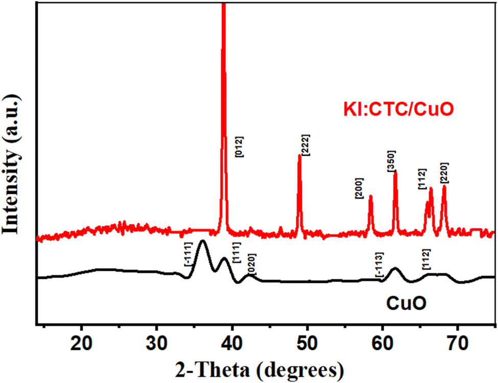 | ||
| Fig. 4 XRD of CuO and KI:CTC/CuO films. | ||
The XRD spectrum of the KI:CTC/CuO bilayers is depicted in Fig. 4 (red curve). The presence of narrow, highly intense peaks in the KI:CTC/CuO spectrum indicates enhanced crystallinity of the bilayer structure. According to JCPDS cards #07-0197 and #75-0376, Cs2SnCl6 crystallizes in a cubic structure with the Fm![[3 with combining macron]](https://www.rsc.org/images/entities/char_0033_0304.gif) m space group, where Sn adopts the +4 oxidation state.26–29 Distinct XRD peaks corresponding to Cs2SnCl6 are observed at 2θ angles of 58.31°, 39.07°, 68.01°, and 66.28°, indexed to the [200], [012], [220], and [112] crystallographic planes, respectively.26–29
m space group, where Sn adopts the +4 oxidation state.26–29 Distinct XRD peaks corresponding to Cs2SnCl6 are observed at 2θ angles of 58.31°, 39.07°, 68.01°, and 66.28°, indexed to the [200], [012], [220], and [112] crystallographic planes, respectively.26–29
Furthermore, Fig. 4(b) presents the XRD data, which reveal the orthorhombic structure of KI, with peaks observed at 2θ angles of 61.45° and 48.83°, corresponding to the [350] and [222] planes, respectively. This agrees with card #01-0796, confirming the successful doping of KI into CTC.30,31 The crystal size of KI:CTC/CuO is estimated to be approximately 37.73 nm. The high-quality crystal structure of the bilayers in the photodetector plays a significant role in enhancing its stability and durability.
3.3. Optical analysis
Fig. 5 (black color) presents an analysis of the optical properties of the CuO layer. The figure displays several optical parameters, including absorbance (A), transmittance (T), reflectance (R), and band gap (Eg). In Fig. 5(a), the absorbance curve of the CuO layer shows a prominent peak. This peak is located in the UV-visible range. It arises from electronic photoexcitation from the valence band (VB) to the conduction band (CB). Notably, the CuO absorption rapidly between 400 and 520 nm and reaches a steady state. Additionally, the absorption peak at 840 nm can be attributed to the increased thickness of the CuO layer, resulting in extended absorption into the near-infrared region.32,33 | ||
| Fig. 5 Optical properties of CuO and KI:CTC/CuO: (a) absorbance, (b) transmittance, (c) reflectance, and (d) band gap. | ||
Fig. 5(b) demonstrates that the transmittance of CuO is initially close to zero for wavelengths exceeding 430 nm. Subsequently, there is an exponential increase in transmittance with wavelength until it reaches a plateau state at λ > 600 nm. The reflectance spectrum in Fig. 5(c) shows low values, indicating significant absorption of the CuO layer in the UV-visible regions. Additionally, the reflectance spectrum displays oscillating interference fringes associated with the CuO layer.34
The absorption coefficient (α) can be determined using the film thickness (d) and absorbance (A), as expressed in the next equation35
| α = 2.3(A/d) | (1) |
The optical band gap (Eg) can be calculated by using Tauc model
 | (2) |
The optical properties of a bilayer composed of KI:CTC/CuO are discussed in Fig. 5 (red color). In Fig. 5(a), the absorbance measurements demonstrate that the KI:CTC/CuO bilayer efficiently absorbs light in the 400 to 800 nm wavelength range. Consequently, this bilayer exhibits a redshift towards the visible light spectrum, showing higher absorbance compared to the CuO film. This indicates an increase in photon absorption, leading to enhanced production of charge carriers.36 Fig. 5(b) demonstrates the transmittance characteristics of the bilayer, showing close to zero transmittance for wavelengths shorter than λ > 400 nm and exponential growth as wavelength increases. Beyond λ > 600 nm, the transmittance reaches a plateau. This indicates high opacity to UV and visible light and increasing transparency at longer wavelengths. Fig. 5(c) shows that the KI:CTC/CuO bilayer has lower reflectance than the CuO layer, particularly in the UV-visible regions. The reduced reflectance is attributed to effective light modulation at the interfaces of the KI:CTC layer.37
Fig. 4(d) provides information about the band gap of the KI:CTC/CuO, which is measured at 1.55 eV, indicating its suitability for various optoelectronic applications due to this relatively low band gap. While materials with larger band gaps primarily absorb light in the UV spectrum, which can limit their effectiveness in detecting visible or infrared light. The high-band-gap materials have significant applications in UV photodetection.38 These include environmental monitoring, UV sterilization, and detecting emissions from UV sources like LEDs and lamps.39 Additionally, they are crucial in health and safety applications, such as monitoring UV exposure to prevent skin damage.40 Furthermore, these materials are vital for space-based applications, contributing to studies of solar activity and its effects on Earth's atmosphere.41 The development of sensors utilizing these materials can enhance photonic devices for UV imaging and spectrometry.42
The optical bandgap decreases when CuO is combined with KI:CTC, as seen in Fig. 5(d). This can be attributed to band structure modification and interfacial interactions between the two materials. The formation of a heterojunction leads to energy level alignment, which reduces the overall optical bandgap. Additionally, charge transfer effects and localized states at the interface may introduce intermediate energy states within the band structure, further lowering the effective bandgap. Furthermore, the increased surface roughness enhances light interaction with the KI:CTC/CuO structure by expanding the surface area, resulting in greater light scattering and trapping, ultimately improving the material's optical properties. As a result, the efficient light absorption and relatively low bandgap value of KI:CTC/CuO indicate the potential of the KI:CTC/CuO bilayer in photodetector applications.
3.4. KI:CTC/CuO photodetector
 | ||
| Fig. 6 (a) Effect of the light power density on the photocurrent values (b) the relationship between the photocurrent values and the light power at +1 V for the KI:CTC/CuO photodetector. | ||
With an increase in power intensity of incident white light (from 25.0 to 100.0 mW cm−2), the photocurrent (Jph) of the KI:CTC/CuO bilayers also increases. The photo-excited current is 67.5 times higher than the dark current at a fixed bias of 1 V. The values of photocurrent are high enough for direct measurement without any amplifier. When the bilayers are illuminated, the electrons absorb the energy from the incident light and transition from VB to CB. This process creates electron–hole pairs (e–h). The photo-generated carriers are efficiently separated due to the presence of an applied bias voltage. The holes tend to migrate towards the surface, where they interact with the adsorbed oxygen ions. Hence, holes remove negative charges and discharge the oxygen ions. So, the desorption of O2 ions is facilitated by the presence of holes. Consequently, the conductivity of the KI:CTC/CuO bilayers improves. This leads to a reduction in resistance and an increase in photocurrent under light illumination. The photocurrent rises as the applied voltage increases due to the faster drift velocity and increase in photogenerated electron–hole pair separation.
Fig. 6(b) presents the relationship between photocurrent density (Jph) and light power intensity (P) at +1.0 V for the KI:CTC/CuO bilayers. The photocurrent density increases from 8.66 to 13.56 mA cm−2 as the power intensity rises from 25.0 to 100.0 mW cm−2. This demonstrates the strong dependence of the generated photocurrent on the light power intensity. With an increase in light intensity, more electrons within the KI:CTC/CuO bilayers are excited from VB to CB. Consequently, additional charge carriers (electron–hole pairs) are generated on the surface of the material. This increased availability of carriers contributes to the observed higher photocurrent.
It is important to note that the relationship between incident light intensity and the resulting photocurrent density is nonlinear. This nonlinearity indicates the complexity of the electron–hole transportation reaction occurring in the KI:CTC/CuO bilayers. Several factors may influence the overall photocurrent response, such as carrier recombination, trapping, or other transport mechanisms. These factors can affect the efficiency of charge carrier generation, transport, and collection, leading to the photocurrent density does not increase proportionally with an increase in incident light intensity.45
The relationship between Jph and P for the KI:CTC/CuO bilayers can be described using the power-law equation
| Jph = CPk | (3) |
 | ||
| Fig. 7 (a) The relationship between the photocurrent values and the voltage in the presence of several wavelengths and (b) the correlation of Jph – λ at +1 V for KI:CTC/CuO photodetector. | ||
The photocurrent–voltage measurement across a range of monochromatic wavelengths is presented in Fig. 7(a). This analysis covers wavelengths from 390 to 636 nm, with the light intensity for all different wavelengths maintained at a constant 75.0 mW cm−2. As the wavelengths increase, the Jph values decrease. Fig. 7(b) further illustrates this correlation by plotting the photocurrent values at +1 V against different monochromatic light sources during illumination. According to Fig. 7(b), the photocurrent density decreases non-linearly as the incident light wavelength increases. Specifically, the photocurrent density at a wavelength of 390.0 nm is 12.8 mA cm−2, while at 636.0 nm, it drops to 3.4 mA cm−2. This decrease in photocurrent is due to the longer wavelengths of light carry lower energy photons. These lower energy photons possess a reduced ability to excite electrons across the energy bandgap of the material. Consequently, the diminished excitation of electrons leads to a reduction in photocurrent. The high photocurrent observed under short-wavelength light irradiation in the UV region attributed to the increased generation of e/h pairs. This occurs when the photon energy exceeds the bandgap of the bilayer, leading to a greater number of photo-generated carriers. This indicates the photoresponse strongly depends on the photon wavelength. This proves the broadband detection capability from ultraviolet to the visible range.
The photoresponsivity (PR) is a crucial factor for evaluating the performance of a photodetector. PR denotes the ratio of the generated photocurrent to the incident light power on the effective area of the photodetector. The calculation is performed using the following equation.48,49
 | (5) |
The photoresponsivity is determined by analyzing the relationship between light intensity and photocurrent density at a specific applied voltage. Fig. 8(a) displays the PR values for different applied wavelengths at +1 V. Notably, the maximum PR of 143 mA W−1 is observed at 390 nm, which agrees with the Jph results depicted in Fig. 7(b). The PR is lower in the visible region compared to the UV region due to factors such as reduced absorption and shorter recombination time in that range.
 | ||
| Fig. 8 (a) The relationship between photoresponsivity–wavelengths and (b) the EQE under different intensities of light illumination for the KI:CTC/CuO photodetector. | ||
External quantum efficiency (EQE) is a key factor that measures the efficiency of a photodetector in converting incident light photon flux into photocurrent.50,51 The flux of photons is directly proportional to the intensity of the incident light. EQE is defined as the ratio of the number of generated charge carriers to the number of incident photons. The bandgap and absorption coefficient of the photodetector material influence its EQE. A higher EQE value corresponds to a more efficient photodetector that can convert a larger fraction of incident photons into detectable charge carriers. High EQE generally leads to higher D*. The EQE can be determined using the next equation52
 | (7) |
Based on Fig. 8(b), it can be observed that the external quantum efficiency (EQE) of the KI:CTC/CuO perovskite bilayer decreases from 61.0% to 30.0% as the wavelength increases from 390.0 nm to 636.0 nm. This trend indicates a reduction in the efficiency of converting incident photons into electric current as the wavelength of light increases, which agrees with the responsivity (PR) values in Fig. 8(a).
Detectivity (D*) is a valuable parameter used for comparing the performance of different photodetectors under specific conditions, such as a particular wavelength and bandwidth. It quantifies the minimum detectable signal that the photodetector can reliably differentiate from the noise level. This characteristic is important for applications that require the detection of weak light signals in the presence of background noise, such as in astronomy, night vision systems, medical imaging, optical communication, and sensing. The detectivity can be calculated using eqn (6) (ref. 49)
 | (6) |
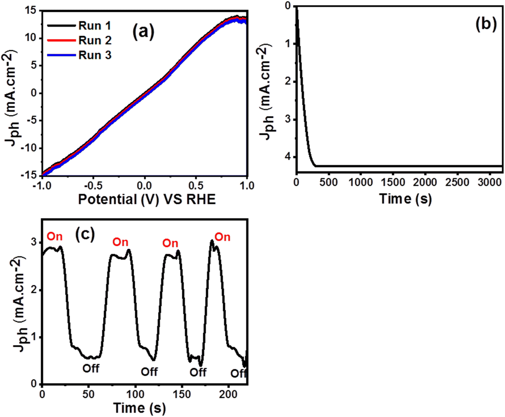 | ||
| Fig. 9 (a) Reproducibility (b) stability, and (c) chopping current of the KI:CTC/CuO photodetector. | ||
Stability refers to the photodetector's ability to maintain a consistent and reliable response over an extended duration, which is crucial for long-term performance and reliability. Factors such as aging of components, degradation of materials, operating conditions, and electronic drift can affect the stability. To assess the stability of the KI:CTC/CuO photodetector, chronoamperometry was performed. This technique involves applying a voltage of 1.0 V and measuring the photocurrent values under a light intensity of 100.0 mW cm−2. By monitoring the photocurrent over an extended period, the stability of the photodetector can be evaluated. Analysis of Fig. 9(b) reveals that the photocurrent values initially decreased during the first 270 seconds, followed by a nearly constant level maintained until 500 seconds. These findings indicate an acceptable level of stability for the prepared KI:CTC/CuO photodetector. The presence of oxygen molecules adsorbed on the KI:CTC/CuO surface contributes to a relatively small change in the photocurrent values over time. The use of stable inorganic materials in the construction of the KI:CTC/CuO photodetector significantly contributes to its high stability.53 The improved crystallinity and low defect density in the KI:CTC/CuO bilayers enhance the stability of photodetector applications' performance over an extended period. The high-quality crystal structure of the bilayers enhances charge transport properties, promotes efficient carrier generation, and reduces charge carrier recombination, resulting in stable photodetection capabilities. This also exhibits enhanced durability and decreases the chances of performance degradation or failure.
On/off light chopping is a technique used to achieve more precise measurement and analysis of the photodetector's performance by isolating the photocurrent generated by the incident light. This technique involves alternating between periods of white illumination provided by the xenon lamp (light-on at 100 mW cm−2) and darkness (light-off at 0 mW cm−2). By using this technique, the signal of interest (the photocurrent generated by the incident light) can be separated from other sources of current, such as dark current or background noise. The transient photocurrent response to on/off illumination is exhibited in Fig. 9(c), where three cycles were measured. Good repeatable photocurrent generation indicates that the photoresponse of the photodetector is reversible, and the photocurrent remains stable without degradation. When the light is turned on, the photocurrent rapidly increases to its maximum value and remains stable. Conversely, when the light is turned off, the photocurrent drastically drops back to its initial value.
The on/off ratio, defined by the photocurrent/dark current (on/off = Jph/Jdark), is another factor parameter of the photodetector. A high on/off ratio is desirable for practical applications of KI:CTC/CuO as a high-quality photosensitive switch. At an applied voltage of +1.0 V, the photodetector exhibits an on/off (Jphoto/Jdark) ratio of approximately 3.0. The rapid increase in current and the stable value achieved demonstrate fast charge transfer and reliable performance.
The rise and decay times are critical parameters for evaluating the response speed of the photodetector. During the illumination on/off cycle, the rise time and decay time are defined as the time required for the photocurrent to transition from 10% to 90% and 90% to 10%, respectively, of its stable value. The calculated rise time is 20.0 s, while the decay time is 34.0 s, enabling effective detection and analysis of light signals. The observed hysteresis and delayed response during the switching process result from the complex charge generation and transport dynamics during the on/off cycles, which do not follow a linear pathway. This behavior suggests energy retention within the material, potentially affecting measurement accuracy and precision.54,55
As a result, the photodetector holds strong potential for practical applications involving the detection of many wavelengths and light power intensities. Its competitive characteristics make it a promising choice in the field. Lastly, Table 1 compares the performance of the presented KI:CTC/CuO photodetector with earlier research.
| Structure | Wavelength (nm) | Bais (V) | R (A W−1) | D (Jone) |
|---|---|---|---|---|
| Cu2O/ZnO56 | 596 | 0 | 0.288 × 10⁻³ | — |
| n-Cu2O/p-CuI57 | 465 | 0 | 0.25 | — |
| TiO2/CsSnI3/P3HT58 | 350–1000 | 0 | 0.257 | 1.5 × 10¹⁰ |
| CsSnI3 (ref. 59) | 940 | 0.1 | 0.054 | 3.85 × 10⁵ |
| GO/Cu2O60 | 300 | 2 | 0.0005 | 1.0 × 10⁶ |
| Cs2SnI6 (ref. 61) | — | 3 | — | — |
| CuO nanowires12 | 390 | 5 | — | — |
| CuO/Si Nanowire14 | 405 | 0.2 | 3.8 × 10⁻³ | — |
| ZnO–CuO62 | 405 | 1 | 3 × 10⁻³ | — |
| CuFeO2/CuO/Cu63 | 390 | 1 | 0.33 | — |
| Cu/CuO NP64 | 390 | 1 | 6.2 × 10⁻³ | — |
| KI:CTC/CuO (this work) | 400 | 1 | 0.143 | 7.95 × 10⁹ |
4. Mechanism
Fig. 10 illustrates the energy diagram of the KI:CTC/CuO photodetector system and the charge transfer mechanisms. When the semiconductor material (either KI:CTC or CuO) absorbs suitable photons, it excites electrons from the VB to the CB, creating e/h pairs. The KI:CTC/CuO bilayer enhances light absorption and e/h pair generation due to its low band gap, rough surface texture, and large surface area. However, the recombination of e/h pairs can decrease carrier mobility and hinder their contribution to the photocurrent.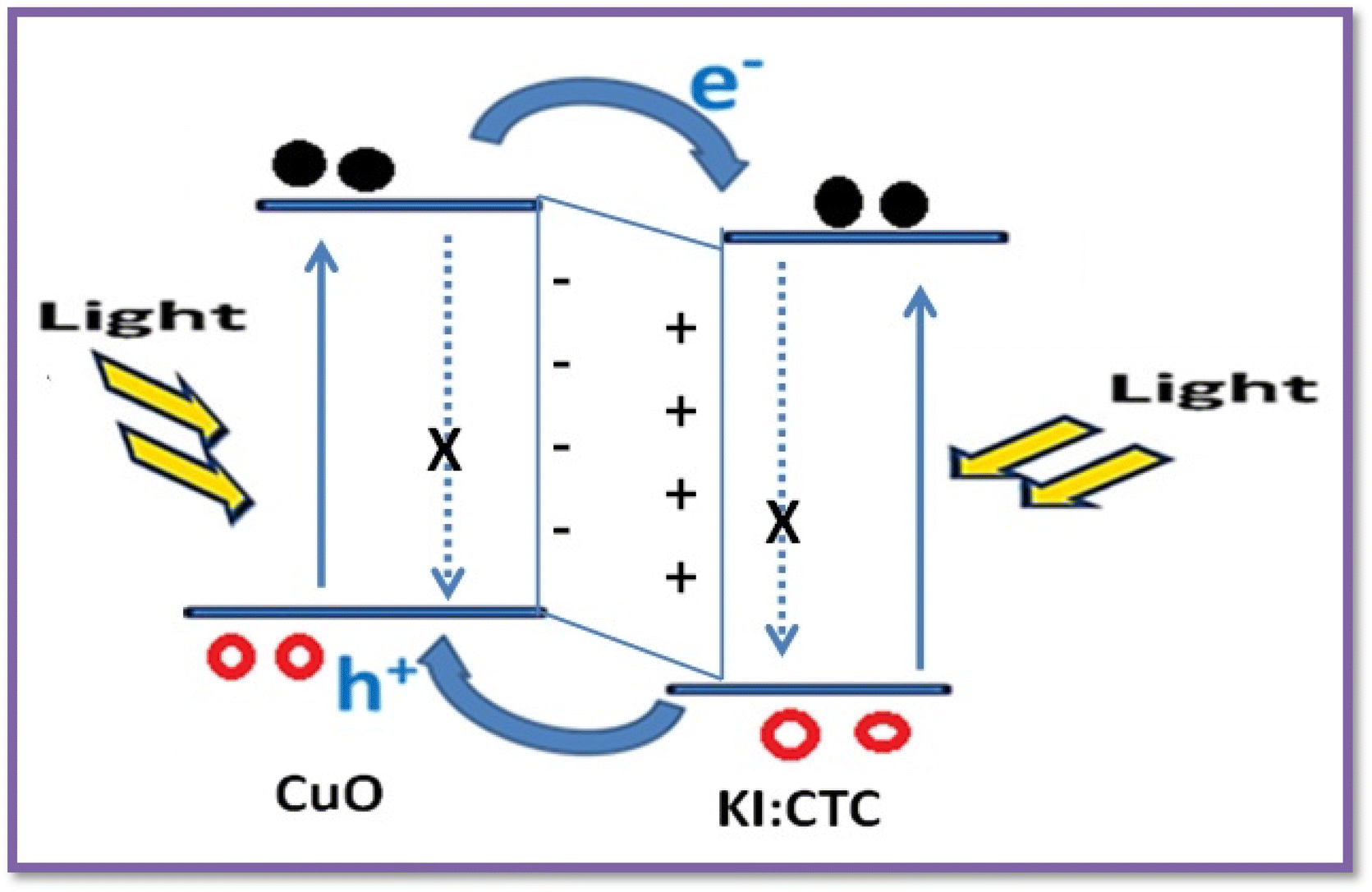 | ||
| Fig. 10 Energy diagram of the KI:CTC/CuO photodetector system. | ||
At the interface between the KI:CTC and CuO layers, charge transfer occurs. Carrier diffusion between CuO and KI:CTC continues until the Fermi energy levels (EF) of both materials reach equilibrium. This results in band bending of the electronic structure and the formation of a depleted region at the KI:CTC/CuO junction. Consequently, a pn junction is formed between the n-type CuO and p-type Cs2SnCl6 (KI:CTC), creating a built-in electric field. Under the influence of this internal electric field, electrons from CuO migrate to the CB of KI:CTC, while holes generated in KI:CTC move to the VB of CuO. The built-in electric field thus acts as a potential barrier that separates e/h pairs more quickly and effectively.65 In addition, the interface between the Ag electrodes and the KI:CTC/CuO layer can be crucial for optimizing charge transfer. The work function of silver can significantly influence the energy barrier for carrier injection, helping to create a built-in electric field that efficiently separates and collects photogenerated charges.65 The junction's ability to improve light absorption leads to the creation of additional free carriers.66 Moreover, the internal electric field facilitates carrier transfer and electron accumulation on the surface of KI:CTC. Consequently, the KI:CTC/CuO structure demonstrates an improved photoresponse, resulting in an increased photocurrent value.
The efficiency of the KI:CTC/CuO photodetector can be further enhanced by incorporating potassium iodide (KI) into the system. While pure Cs2SnCl6 has its merits, it lacks the enhanced properties that KI brings to the table, such as improved absorption characteristics, better carrier mobility, and overall stability. KI modifies the band alignment of the perovskite material, reducing the charge-transfer barrier and improving conductivity.67,68 This enhancement facilitates more efficient charge transfer and higher photocurrent generation. Consequently, the photodetector exhibits high performance, making the KI:CTC/CuO photodetector well-suited for a variety of industrial applications.
5. Conclusion
In this study, a high-efficiency KI-doped Cs2SnCl6 (KI:CTC)/CuO bilayer was synthesized for photodetector applications. The KI:CTC/CuO bilayers were tested over a range of light intensities from 25.0 to 100.0 mW cm−2 and wavelengths from 390.0 to 636.0 nm. Various techniques were used to characterize the optical, chemical, and morphological properties of the bilayers. The KI:CTC/CuO bilayers exhibited good crystallinity and a low bandgap (Eg). Notably, the photoresponsivity of the bilayers was measured to be 143 mA W−1, with an external quantum efficiency of 61.0% and a high detectivity of 7.95 × 10⁹ Jones. The impressive performance demonstrated by the synthesized KI:CTC/CuO bilayer opens up exciting opportunities for its utilization across numerous fields and a wide range of technological applications.Data availability
Data will be made available on request.Author contributions
A. H. Ali: writing – original draft, methodology, formal analysis. A. M. Ahmed: formal analysis, data curation, software. S. M. Abass: investigation, visualization. A. A. Abdel-Khaliek: investigation, supervision. M. Shaban: resources, investigation. M. Al-Hmoud: data curation, visualization. S. Abd El Khalik: resources, visualization. M. Rabia: conceptualization, formal analysis, software.Conflicts of interest
The authors declare that they have no known competing financial interests or personal relationships that could have appeared to influence the work reported in this paper.Acknowledgements
This work was supported and funded by the Deanship of Scientific Research at Imam Mohammad Ibn Saud Islamic University (IMSIU) (grant number IMSIU-DDRSP2503).References
- J. Park and K. Hong, Dual-site compositional engineering of bismuth-based halide perovskites for stable and efficient lead-free solar cells, J. Phys. Chem. C, 2021, 125(24), 13138–13145 CrossRef CAS
.
- F. Arjmand, Z. Golshani, S. Fatemi, S. Maghsoudi, A. Naeimi and S. Hosseini, The lead-free perovskite solar cells with the green synthesized BiI3 and AgI nanoparticles using Vitex agnus-castus plant extract for HTM-free and carbon-based solar cells, J. Mater. Res. Technol., 2022, 18, 1922–1933 CrossRef CAS
- S. Ghosh, H. Shankar and P. Kar, Recent developments of lead-free halide double perovskites: a new superstar in the optoelectronic field, Mater. Adv., 2022, 3(9), 3742–3765 RSC
- A. Rahman, et al., Enhancing the photo-response of CuO thin film based infrared light photodetector via fabricating ZnO-capped CuO device, Phys. B, 2025, 697, 416713 CrossRef CAS
- S. Boriskina, J. Zhou, W. Hsu, B. Liao and G. Chen, Limiting efficiencies of solar energy conversion and photo-detection via internal emission of hot electrons and hot holes in gold, SPIE, 2015, 9608, 299–305 Search PubMed
- D. Ninh, et al., Highly efficient photon energy conversion and ultrasensitive self-powered photodetection via a monolithic p-3C-SiC nanothin film on p-Si/n-Si double junction, ACS Appl. Mater. Interfaces, 2024, 16(29), 38658–38668 CrossRef CAS PubMed
- M. Hayat and R. Khalil, A DFT engineering of double halide type perovskites Cs2SiCl6, Cs2GeCl6, Cs2SnCl6 for optoelectronic applications, Solid State Commun., 2023, 361, 115064 CrossRef CAS
- K. Bouferrache, et al., Crystal structure, mechanical, electronic, optical and thermoelectric characteristics of Cs2MCl6 (M= Se, Sn, Te and Ti) cubic double perovskites, Results Phys., 2024, 56, 107138 CrossRef
- I. Erdogan and O. Gullu, Optical and structural properties of CuO nanofilm: its diode application, J. Alloys Compd., 2010, 492(1–2), 378–383 CrossRef CAS
- Q. Zhang, et al., CuO nanostructures: synthesis, characterization, growth mechanisms, fundamental properties, and applications, Prog. Mater. Sci., 2014, 60, 208–337 CrossRef CAS
- K. Nomura, H. Ohta, A. Takagi, T. Kamiya, M. Hirano and H. Hosono, Room-temperature fabrication of transparent flexible thin-film transistors using amorphous oxide semiconductors, Nature, 2004, 432(7016), 488–492 CrossRef CAS
- S. Wang, et al., A CuO nanowire infrared photodetector, Sens. Actuators, A, 2011, 171(2), 207–211 CrossRef CAS
- Z. Bai and Y. Zhang, Self-powered UV–visible photodetectors based on ZnO/Cu2O nanowire/electrolyte heterojunctions, J. Alloys Compd., 2016, 675, 325–330 CrossRef CAS
- Q. Hong, Y. Cao, J. Xu, H. Lu, J. He and J. Sun, Self-powered ultrafast broadband photodetector based on p–n heterojunctions of CuO/Si nanowire array, ACS Appl. Mater. Interfaces, 2014, 6(23), 20887–20894 CrossRef CAS PubMed
- M. Saidaminov, et al., Inorganic lead halide perovskite single crystals: phase-selective low-temperature growth, carrier transport properties, and self-powered photodetection, Adv. Opt. Mater., 2017, 5(2), 1600704 CrossRef
- Z. Li, et al., Cs2AgBiBr6-based heterojunction photodetector for weak-light imaging application, Surf. Interfaces, 2022, 29, 101705 CrossRef CAS
- F. Cao, Z. Li, X. Liu, Z. Shi and X. Fang, Air induced formation of Cs3Bi2Br9/Cs3BiBr6 bulk heterojunction and its dual-band photodetection abilities for light communication, Adv. Funct. Mater., 2022, 32(46), 2206151 CrossRef CAS
- S. Baturay, A. Tombak, D. Batibay and Y. Ocak, n-Type conductivity of CuO thin films by metal doping, Appl. Surf. Sci., 2019, 477, 91–95 CrossRef CAS
- M. Zhao, Q. Zhao, J. Qiu, H. Xue and H. Pang, Tin-based nanomaterials for electrochemical energy storage, RSC Adv., 2016, 6(98), 95449–95468 RSC
- A. Akbulatov, et al., Comparative intrinsic thermal and photochemical stability of Sn (II) complex halides as next-generation materials for lead-free perovskite solar cells, J. Phys. Chem. C, 2019, 123(44), 26862–26869 CrossRef CAS
- R. Saad, et al., Enhanced CO2 gas sensing at room temperature using Ag-plated Na-doped CuO thin films synthesized by successive ionic layer adsorption and reaction technique, Surf. Interfaces, 2024, 44, 103789 CrossRef CAS
- N. Planken, W. Kautek and T. Dimo, Aqueous Spray Pyrolysis of Cu2O Films: Influence of Reducing Agent and Acetic Acid Addition, ChemNanoMat, 2020, 6(4), 663–671 CrossRef
- M. Dosa, et al., Cerium-Copper Oxides Synthesized in a Multi-Inlet Vortex Reactor as Effective Nanocatalysts for CO and Ethene Oxidation Reactions, Catalysts, 2022, 12(4), 364 CrossRef CAS
- A. Ali, et al., Synthesis of lead-free Cu/CuFeO2/CZTS thin film as a novel photocatalytic hydrogen generator from wastewater and solar cell applications, Opt. Quantum Electron., 2024, 56(5), 1–22 Search PubMed
- M. Migahed, M. El-Rabiei, H. Nady, H. Gomaa and E. Zaki, Corrosion inhibition behavior of synthesized imidazolium ionic liquids for carbon steel in deep oil wells formation water, J. Bio- Tribo-Corros., 2017, 3, 1–20 CrossRef
- G. Xiong, et al., Highly efficient and stable broadband near-infrared-emitting lead-free metal halide double perovskites, J. Mater. Chem. C, 2021, 9(38), 13474–13483 RSC
- S. Lim, H. Lin, W. Tsai, H. Lin, Y. Hsu and H. Tuan, Binary halide, ternary perovskite-like, and perovskite-derivative nanostructures: hot injection synthesis and optical and photocatalytic properties, Nanoscale, 2017, 9(11), 3747–3751 RSC
- A. Ali, et al., Preparation of inorganic lead-free CuO/Cs2SnCl6-KI perovskite for green hydrogen production from wastewater by using solar energy, J. Photochem. Photobiol., A, 2023, 445, 115102 CrossRef CAS
- H. Gomaa, M. El-Rabiei, H. Nady, E. Zaki and M. Migahed, 1-(2-Aminoethyl)-1-dodecyl-2-undecyl-4, 5-dihydro-1 H-imidazole-1-ium chloride, 1-(2-Aminoethyl)-1-dodecyl-2-tridecyl-4, 5-dihydro-1 H-imidazole-1-ium chloride as Corrosion Inhibitors for Carbon Steel in Oil Wells Formation Water, Z. fur Phys. Chem., 2019, 233(11), 1529–1552 CrossRef CAS
- A. Liu, et al., Room-temperature solution-synthesized p-type copper (I) iodide semiconductors for transparent thin-film transistors and complementary electronics, Adv. Mater., 2018, 30(34), 1802379 CrossRef PubMed
- D. Sarma, C. Malliakas, K. Subrah, S. Islam and M. Kanatzidis, K2xSn4−xS8−x (x= 0.65–1): a new metal sulfide for rapid and selective removal of Cs+, Sr2+ and UO22+ ions, Chem. Sci., 2016, 7(2), 1121–1132 RSC
- Z. Chen, et al., Thin single crystal perovskite solar cells to harvest below-bandgap light absorption, Nat. Commun., 2017, 8(1), 1890 CrossRef PubMed
- A. Ali, et al., Preparation and Characterization of Nanostructured Inorganic Copper Zinc Tin Sulfide-Delafossite Nano/Micro Composite as a Novel Photodetector with High Efficiency, Photonics, 2022, 9(12), 979 CrossRef CAS
- N. Lopez, F. Rodriguez, M. Hernandez, F. Flores and S. Jimenez, Dual-doped CdSe:Cu:O films grown by sputtering using CdSe-CuO composite targets, J. Phys.:Condens. Matter, 2020, 32(19), 195701 CrossRef CAS PubMed
- C. Chen, W. Yu, T. Liu, S. Cao and Y. Tsang, Graphene oxide/WS2/Mg-doped ZnO nanocomposites for solar-light catalytic and anti-bacterial applications, Sol. Energy Mater. Sol. Cells, 2017, 160, 43–53 CrossRef CAS
- D. Ju, X. Jiang, H. Xiao, X. Chen, X. Hu and X. Tao, Narrow band gap and high mobility of lead-free perovskite single crystal Sn-doped MA3Sb2I9, J. Mater. Chem. A, 2018, 6(42), 20753–20759 RSC
- A. Nazligul, M. Wang and K. Choy, Recent development in earth-abundant kesterite materials and their applications, Sustainability, 2020, 12(12), 5138 CrossRef CAS
- E. Hamden, et al., Charge-coupled devices detectors with high quantum efficiency at UV wavelengths, J. Astron. Telesc. Instrum. Syst., 2016, 2(3), 036003 CrossRef
- A. Kumar, M. Khan and M. Kumar, Recent advances in UV photodetectors based on 2D materials: A review, J. Phys. D:Appl. Phys., 2021, 55(13), 133002 CrossRef
- A. Perveen, et al., Solution processed and highly efficient UV-photodetector based on CsPbBr3 perovskite-polymer composite film, J. Photochem. Photobiol., A, 2022, 426, 113764 CrossRef CAS
- A. Khan, et al., Advancements in the stability, protection and lead-free strategies of perovskite solar cells: A critical review, Environ. Sci.:Adv., 2024, 3(7), 1004–1029 CAS
- M. Malik, M. Iqbal, J. Choi and P. Pham, 2D materials for efficient photodetection: Overview, mechanisms, performance and UV-IR range applications, Front. Chem., 2022, 10, 905404 CrossRef CAS PubMed
- N. Shinde, P. Deshmukh, S. Patil and C. Lokhande, Development of polyaniline/Cu2ZnSnS4 (CZTS) thin film based heterostructure as room temperature LPG sensor, Sens. Actuators, A, 2013, 193, 79–86 CrossRef CAS
- C. Chen, W. Yu, T. Liu, S. Cao and Y. Tsang, Graphene oxide/WS2/Mg-doped ZnO nanocomposites for solar-light catalytic and anti-bacterial applications, Sol. Energy Mater., 2017, 160, 43–53 CrossRef CAS
- X. Wang, W. Tian, M. Liao, Y. Bando and D. Golberg, Recent advances in solution-processed inorganic nanofilm photodetectors, Chem. Soc. Rev., 2014, 43(5), 1400–1422 RSC
- L. Luo, et al., Light trapping and surface plasmon enhanced high-performance NIR photodetector, Sci. Rep., 2014, 4(1), 1–8 Search PubMed
- H. Zhao, B. Ouyang, L. Han, Y. Mishra, Z. Zhang and Y. Yang, Conjuncted photo-thermoelectric effect in ZnO–graphene nanocomposite foam for self-powered simultaneous temperature and light sensing, Sci. Rep., 2020, 10(1), 1–11 CrossRef PubMed
- S. Kunwar, S. Pandit, J. Jeong and J. Lee, Improved photoresponse of UV photodetectors by the incorporation of plasmonic nanoparticles on GaN through the resonant coupling of localized surface plasmon resonance, Nano-Micro Lett., 2020, 12(1), 1–16 CrossRef PubMed
- R. Jia, D. Zhao, N. Gao and D. Liu, Polarization enhanced charge transfer: dual-band GaN-based plasmonic photodetector, Sci. Rep., 2017, 7(1), 1–8 CrossRef PubMed
- S. Bell, G. Will and J. Bell, Light intensity effects on photocatalytic water splitting with a titania catalyst, Int. J. Hydrogen Energy, 2013, 38(17), 6938–6947 CrossRef CAS
- M. El-Rabiei, G. AbdElHafez and A. Ali, Effects of Alloying Elements (Ti and x Al) on the Electrochemical Corrosion Behaviour of Iron-Based Alloys in Corrosive Solutions of Different pH, J. Bio- Tribo-Corros., 2020, 6, 1–16 CrossRef
- M. Shaban, M. Rabia, A. Abd ElSayed, A. Ahmed and S. Sayed, Photocatalytic properties of PbS/graphene oxide/polyaniline electrode for hydrogen generation, Sci. Rep., 2017, 7(1), 1–13 CrossRef CAS PubMed
- M. Fadel, M. Rabia, S. Ezzat, N. Mansour, E. Saeed and S. Sayyah, Effect of annealing temperature on VO2(M)/ITO film nanomaterials for thermochromic smart windows application and study its contact angle, Nanophotonics, 2018, 12(1), 016009 Search PubMed
- N. Huo and G. Konstantatos, Recent progress and future prospects of 2D-based photodetectors, Adv. Mater., 2018, 30(51), 1801164 CrossRef PubMed
- P. Martyniuk, J. Antoszewski, M. Martyniuk, L. Faraone and A. Rogalski, New concepts in infrared photodetector designs, Appl. Phys. Rev., 2014, 1(4), 041102 Search PubMed
- D. Guo, W. Li, D. Wang, B. Meng, D. Fang and Z. Wei, High performance Cu2O film/ZnO nanowires self-powered photodetector by electrochemical deposition, Chin. Phys. B, 2020, 29(9), 098504 CrossRef CAS
- H. Madusanka, H. Herath and C. Fernando, High photoresponse performance of self-powered n-Cu2O/p-CuI heterojunction based UV-Visible photodetector, Sens. Actuators, A, 2019, 296, 61–69 CrossRef CAS
- F. Cao, W. Tian, M. Wang, M. Wang and L. Li, Stability enhancement of lead-free CsSnI3 perovskite photodetector with reductive ascorbic acid additive, InfoMat, 2020, 2(3), 577–584 CrossRef CAS
- M. Han, et al., Controllable growth of lead-free all-inorganic perovskite nanowire array with fast and stable near-infrared photodetection, J. Phys. Chem. C, 2019, 123(28), 17566–17573 CrossRef CAS
- T. Lan, A. Fallatah, E. Suiter and S. Padalkar, Size controlled copper (I) oxide nanoparticles influence sensitivity of glucose biosensor, Sens. Actuators, A, 2017, 17(9), 1944 Search PubMed
- X. Han, et al., Lead-free double perovskite Cs2SnX6: facile solution synthesis and excellent stability, Small, 2019, 15(39), 1901650 CrossRef PubMed
- M. Rabia, M. Shaban, B. Jibali and A. Abdelkhaliek, Effect of annealing temperature on the photoactivity of ITO/VO2(M)/Au film electrodes for water splitting, Nanosci. Nanotechnol., 2020, 20(7), 4120–4130 CAS
- F. Alkallas, A. Ben, T. Alrebdi, A. Ahmed and M. Rabia, Development of a Highly Efficient Optoelectronic Device Based on CuFeO2/CuO/Cu Composite Nanomaterials, Materials, 2022, 15(19), 6857 CrossRef CAS PubMed
- A. Abdelazeez, et al., Development of CuO nanoporous material as a highly efficient optoelectronic device, Appl. Phys. A:Mater. Sci. Process., 2022, 128(4), 321 CrossRef CAS
- L. Su, W. Yang, J. Cai, H. Chen and X. Fang, Self-powered ultraviolet photodetectors driven by built-in electric field, Small, 2017, 13(45), 1701687 CrossRef PubMed
- M. Zayed, S. Samy, M. Shaban, A. Altowyan, H. Hamdy and A. Ahmed, Fabrication of TiO2/NiO pn nanocomposite for enhancement dye photodegradation under solar radiation, Nanomaterials, 2022, 12(6), 989 CrossRef CAS PubMed
- T. Bu, et al., A novel quadruple-cation absorber for universal hysteresis elimination for high efficiency and stable perovskite solar cells, Energy Environ. Sci., 2017, 10(12), 2509–2515 Search PubMed
- Z. Tang, et al., Hysteresis-free perovskite solar cells made of potassium-doped organometal halide perovskite, Sci. Rep., 2017, 7(1), 12183 CrossRef PubMed
| This journal is © The Royal Society of Chemistry 2025 |