
 Open Access Article
 This Open Access Article is licensed under a Creative Commons Attribution-Non Commercial 3.0 Unported Licence
Controllable growth of wafer-lever MoS2 films by using ex situ heating sulfurization treatment
Mingling Xie ab,
Chaoxin Yunb,
Xiangqian Wangb,
Kaizhou Heb,
Bin Liub,
Jijie Zhaob,
Xiaoping Gaob,
Dongqiang Zhang*a and
Guangan Zhang*c
ab,
Chaoxin Yunb,
Xiangqian Wangb,
Kaizhou Heb,
Bin Liub,
Jijie Zhaob,
Xiaoping Gaob,
Dongqiang Zhang*a and
Guangan Zhang*c
aSchool of Petrochemical Engineering, Lanzhou University of Technology, Lanzhou 730000, China. E-mail: zhangdq@lut.edu.cn
bKey Laboratory of Sensor and Sensing Technology, Institute of Sensing Technology, Gansu Academy of Sciences, Lanzhou 730000, China
cState Key Laboratory of Solid Lubrication, Lanzhou Institute of Chemical Physics, Lanzhou 730000, China. E-mail: gazhang@licp.cas.cn
First published on 7th March 2025
Abstract
Few-layer MoS2 films have garnered significant attention as promising materials for electronic devices and sensors due to their exceptional carrier mobility and tunable bandgap. Although various chemical vapor deposition (CVD) techniques have been employed to fabricate few-layer MoS2 films, there remains a need for film homogeneity, continuity, and crystalline quality improvements. This research used the TVS method to fabricate large-scale few-layered MoS2 films. The metal Mo films were sulfurized under high vacuum conditions using both in situ and ex situ rapid heating techniques. The in situ treatment method resulted in a mixed phase of MoO2–MoS2, whereas the ex situ approach produced uniform and pure polycrystalline 2H-MoS2 films. By adjusting the thickness of the Mo film, a tri-layer 2H-MoS2 film grown on a 2-inch sapphire wafer served as the channel material for a top-gate thin-film transistor (TFT). Electrical measurements indicated an n-type semiconductor behavior with a field-effect mobility of 9.2 cm2 V s and an Ion/Ioff ratio of approximately 102. These results confirm that the ex situ rapid treatment technique effectively grows high-quality, wafer-scale, and layer-controlled few-layer MoS2 films.
1. Introduction
Transition metal dichalcogenides (TMDs) have drawn tremendous attention because of their remarkable chemical, electronic, and physical properties, which have resulted in their potential application in lubrication, catalysis, electronic and optoelectronic devices, sensors, and field-effect transistors (FET).1 Particularly, molybdenum disulfide (MoS2), a representative semiconductor material with excellent catalytic activity, high carrier mobility, and an adjustable bandgap,2,3 has been extensively evaluated as a potential candidate for applications in electronic devices, sensors, and related fields.4–6 These applications have stimulated a high demand for the controllable synthesis of high-quality and large-area continuous few-layer MoS2 films.Currently, some research is focused on the production of large-scale continuous thin films, including exfoliation technologies, chemical vapor deposition (CVD), and physical vapor deposition (PVD).7–9 CVD has been demonstrated as the most effective and convenient technology because of its accessibility and controllable synthesis of MoS2 film. This technology includes thermal vapor deposition (TVD) and thermal vapor sulfurization (TVS).10,11 A few researchers have reported that TVD method can be obtained on diversified substrates by applying the solid vapor reaction of molybdenum trioxide (MoO3) and sublimed sulfur (S) powders. However, few TVD methods can obtain continuous bulk, monolayer, and multilayer MoS2 film by gathering the triangular MoS2 domain on a submicron scale.12 These gathering triangular domains appear discretionary crystal orientation and a few large grain boundaries, which affects the surface uniformity and electrical properties, thereby limiting the device development.13 Furthermore, thermal vapor sulfurization (TVS) is also used to grow MoS2 film, which lies in the type of precursor containing the chalcogen vapors and the pre-deposited transition metal or oxide on substrates by diverse means.14 The nano-films of MoO3 and Mo pre-deposited on the substrates play as the nucleation sites for the crystal growth of MoS2 during the vulcanization reaction.10 The layer of MoS2 film is related to the thickness of pre-deposition Mo film. The MoS2 film achieved by TVS methods, exhibits good uniformity, high controllability, large-scale, and crystallinity.
Recently, the process parameters including precursors and pre-deposited means, reactant gas, pressure and temperature, catalyst, and so on, have been reported as the accurate tuning and optimized process to achieve superior performance for MoS2 films.15,16 The single and few-layer MoS2 film achieved by the sputtering-CVD reaction approach, exhibited a wide area of 150 μm × 150 μm and a high field effect mobility of 12.24 ± 0.741 cm2 V−1 s−1, but the cross-section HRTEM of MoS2 films had a discontinuous layered structure at 600 °C.17 A multi-step heating sulfurization approach was developed to sulfurize the pre-deposited Mo film, which could achieve a continuous layered MoS2 film with a uniform structure. The procedure included five aim temperatures (500 °C, 600 °C, 700 °C, 800 °C, 900 °C).18 A higher annealing temperature can improve the crystallinity of synthesis MoS2 film. Moreover, Pradhan et al. also indicated that hydrogen atoms play an important role in the process of sulfurizing the sputtering Mo film, and observed that the crystallinity of the films increased with the hydrogen flow rate.11 While high crystallinity is advantageous for the performance of electron devices, the surface unevenness and purity of the synthesized MoS2 film also significantly influence its characteristics. The high quality of MoS2 film has been limited by surface homogeneity and purity of the MoS2 films.
In the study, the TVS method was employed to fabricate large-scale few-layered MoS2 films. Firstly, an in situ heating process was used to prepare MoS2 film by sulfurization of pre-sputtered Mo layers. The single MoO2 phase was finally formatted in the process of the in situ heating treatment. To avoid the formation of MoO2 phase, an ex situ heating method was developed to synthesize the uniform and pure 2H-MoS2 films on 2-inch wafers. A top-gate MoS2-based TFT device arrayed on 2-inch sapphire wafer was used to explore the semiconductor properties. This study aims to find an effective method for synthesizing the uniform and large-size MoS2 film that is compatible with micro-electromechanical fabrication processes, which could serve as the groundwork for further research and application of 2D-MoS2 in the field of microelectronic devices.
2. Experimental section
2.1. Preparation and characterization of MoS2
Firstly, metal Mo films were pre-deposited on 300 nm SiO2/Si and sapphire substrates (2-inch wafers) by DC magnetron sputtering. Before the deposition of Mo films, the substrates were ultrasonically cleaned in acetone, alcohol, and deionized water solutions, respectively. Subsequently, a two-inch target of 99.99% purity was employed to fabricate Mo films with various thicknesses, achieved by modulating the sputtering duration. Before the sputtering process, the base pressure of the vacuum chamber was assuredly maintained below 10−6 Pa. During sputtering, the working pressure, Ar flow rate, and DC power were maintained at 1.0 × 10⁻³ Pa, 20 sccm, and 10 W respectively. Thin films of the metal molybdenum, with varying thicknesses, were fabricated by adjusting the sputtering duration to 10 s, 60 s, 120 s, 240 s, and 480 s.Secondly, MoS2 was synthesized by sulfurizing metal Mo films of varying thicknesses in a double-temperature zone vacuum furnace, as illustrated in Fig. 1(a). The in situ heating and ex situ heating methods were used to control the reaction temperature. In brief, Mo films and sulfur powder in quartz boats were placed in C position and A position, which remain unaltered within the vacuum tube. Heaters 1 and 2 are employed to control the precursor reaction temperature and the sulfidation reaction temperature, respectively. For the entire duration of the experiment, Heater 1 remains stationary at position A. Meanwhile, Heater 2 can be moved between positions B and C as necessitated by the experimental demands. During the reaction process, the temperatures of Heater 1 and Heater 2 were set to 230 °C and 700 °C, respectively. The in situ heating and ex situ heating modes were used to control the reaction temperature. Both experimental methods include four distinct stages: purging, heating, reaction, and cooling. The detailed experimental process was shown in Fig. 1(b). The synthesis parameters and positions of the heaters are detailed in Table 1. During these experiments, we utilized a gas-pressure meter to monitor fluctuations in the reaction chamber's pressure. The alkaline spray device, positioned at the front end of the tail gas outlet, was employed to mitigate pollutants produced throughout the experiment.
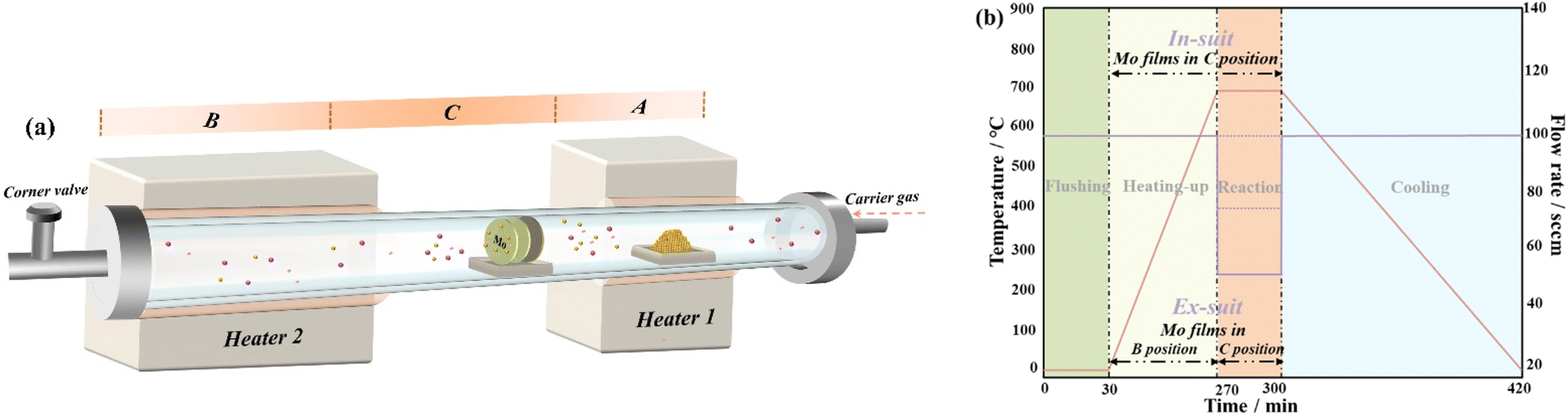 | ||
| Fig. 1 Schematic diagram of TVS method for growing MoS2 films. | ||
| In situ heating method | Ex situ heating method | |||||
|---|---|---|---|---|---|---|
| Time/min | Carrier gas (Ar, H2)/sccm | Heater 2 position | Time/min | Carrier gas/sccm | Heater 2 position | |
| Flushing | 30 | 80, 20 | B | 30 | 80, 20 | B |
| Heating-up | 240 | 80, 20 | C | 240 | 80, 20 | B |
| Reaction | 30 | 10, 2.5 | C | 30 | 10, 2.5 | C |
| Cooling | 120 | 80, 20 | B | 120 | 80, 20 | B |
2.2. Films characterization
The thickness of the Mo films was measured using a variable angle spectroscopic ellipsometer (J.A. Woollam Co., Inc., M-2000U). The structure of the MoS2 films was analyzed with X-ray diffraction (XRD) using Cu Kα radiation (λ = 0.154 nm) at a 1° glancing angle (PANalytical B.V. Empyrean, NL). The chemical structure of the MoS2 films was studied with a laser confocal micro-Raman spectrometer with a 532 nm excitation wavelength (Renishaw in Via, UK). The morphology of the MoS2 films was examined using high-precision optical microscopy (Nikon, MM-400LU) and atomic force microscopy (AFM) (Bruker Dimension ICON).2.3. Device and electrical measurements
The MoS2 films were patterned into a channel for a field-effect transistor (FET) using a UV lithography system (SUSS, MA/BA6 Gen4). Ion beam etching equipment (AVP Technology, RF350) was then used to remove the unwanted portions of the MoS2 films. A magnetron sputtering technique was employed to deposit a Ti/Au/Ti multilayer film (20 nm/150 nm/15 nm), which served as the source, drain, and top-gate electrodes. Additionally, a 20 nm thick SiO2 film was fabricated to function as the dielectric layer for the top-drain.3. Results and discussion
The TVS method, which incorporates both in situ and ex situ heating processes, was utilized to fabricate the large-scale few-layered MoS2 films. The samples derived from the sulfidation of molybdenum metal films, subjected to durations of 10 s, 60 s, 120 s, 240 s, and 480 s, were labeled correspondingly as S1, S2, S3, S4, S5, respectively. Fig. 2 and 3 present the XRD and Raman spectra of in situ sulfurized Mo films under various carrier gas conditions, respectively. In Fig. 2(a), a weak and broad peak corresponding to the amorphous structure is observed in the XRD spectra of the S1 sample, which demonstrate no discernible peaks in the Raman spectra shown in Fig. 3(a). For samples S2, S3, S4, and S5, only the characteristic peaks of MoO2 are detected in the Raman spectra.19 The prominent peaks observed in Fig. 2(a) are associated with the MoO2 phase, consistent with the literature (JCPDS No. 32-0671).20,21 The formation of MoO2 phase is probably attributable to a minimal quantity of S vapor adsorbed on the surface of Mo films and residual oxygen within the quartz tube. To facilitate the reaction between enough S vapor and the Mo films, the carrier gas flow rate was increased to 75 sccm (60 sccm Ar and 15 sccm H2) and 100 sccm (80 sccm Ar and 20 sccm H2). Despite the process adjustments, the phase composition remains only minor alterations, as shown in Fig. 2(b), (c), 3(b) and (c). Most of the diffraction peaks in Fig. 2(b and c) are attributed to the MoO2 phase. Among the samples, the XRD spectra of the S5 sample exhibited a peak corresponding to the MoS2 phase at 49.5° under the carrier gas flow rate of 100 sccm.22 The results were consistent with the Raman spectra. There are two possible explanations for the formation of the mixed phase. First, according to the Mo–O phase diagram, metallic Mo transitions into MoO2 at approximately 500 °C in the presence of a small amount of oxygen. Therefore, we assume that metallic Mo was already converted into the MoO2 phase by heating up to ∼500 °C in situ. However, the issue lies in the insufficient amount of sulfur available for the sulfurization of MoO2. Additionally, the natural oxidation of sputtered Mo films in atmospheric conditions leads to the formation of MoO3. A small fraction of MoS2 may be produced by sulfurizing a mixed phase containing both Mo and MoO3. However, as the reaction time increases, MoS2 may react with MoO3 to form MoO2, as shown in the chemical reaction.22| MoS2 + 6MoO3 = 7MoO2 + SO2 |
 | ||
| Fig. 2 The XRD spectra of in situ sulfurized Mo films under different carrier gas conditions, (a) 40 sccm of Ar and 10 of sccm H2; (b) 60 of sccm Ar and 10 of sccm H2; (c) 80 of sccm Ar and 20 of sccm H2. | ||
 | ||
| Fig. 3 The Raman spectra of in situ sulfurized Mo films under different carrier gas conditions, (a) 40 of sccm Ar and 10 of sccm H2; (b) 60 of sccm Ar and 10 of sccm H2; (c) 80 of sccm Ar and 20 of sccm H2. | ||
To prevent the formation of the MoO2 phase during sulfidation, an ex situ heating method was developed to produce single-phase MoS2 films. The detailed experimental process is illustrated in Fig. 1. In this process, Heater 2 occupies the vacant space (position B) upon heating, and subsequently relocates to the sample position (position C) during the reaction. Fig. 4 presents the phase and crystallinity evaluation of MoS2 films prepared using the ex situ heating method. The XRD spectra obtained after the ex situ treatment are shown in Fig. 4(a). The diffraction peaks observed at 2θ values of 33.35°, 40.65°, and 58.85° correspond to the (101), (103), and (110) lattice planes of the hexagonal MoS2 phase (ICDD 00-002-0132),23,24 respectively, while the peak from the impurity phase has disappeared.
 | ||
| Fig. 4 Structural analysis of ex situ sulfurized Mo films (a) XRD spectra, (b) Raman spectra, (c) PL spectra. | ||
In the Raman spectra, two characteristic peaks associated with MoS2 are exclusively observed in Fig. 4(b), which correspond to the A1g (in-plane vibrational) and E12g (out-of-plane vibrational) modes, respectively.5 It is well known that the thickness of MoS2 films can be accurately assessed by measuring the wavenumber difference between the A1g and E12g peak. Specifically, a wavenumber difference (Δω) of approximately ∼25 cm−1 suggests that the synthesized MoS2 films are in the bulk phase. Conversely, a wavenumber difference below ∼25 cm−1 indicates a two-dimensional structure.7,25 The characteristic peaks of the S2, S3, S4, and S5 samples located at ∼383.3 cm−1 and ∼408.9 cm−1. The wavenumber difference between two typical peaks exceeds 25 cm−1, indicating that the prepared MoS2 films (S2, S3, S4, S5) have a bulk phase structure. In Fig. 4(a), the E12g peak for the S1 sample is observed at 383.3 cm−1, while the A1g peak appears at 406.3 cm−1. The wavenumber difference between these two peaks is 23.0 cm−1, which confirms the presence of a trilayer MoS2 structure.8 Moreover, the intensity ratio of the A1g peak to the E12g peak demonstrates a direct correlation with the thickness of the films. The results obtained from Raman spectra align with the XRD data, thereby confirming the successful synthesis of single-phase MoS2 films via the ex situ heating method.
Generally, the electronic structures of MoS2 have been characterized using photoluminescence (PL) measurements. The electronic properties of MoS2 are closely related to the number of layers. For monolayer MoS2, a strong photoluminescence peak at approximately 652 nm (1.9 eV) corresponds to direct excitonic transition energies.26 As the number of MoS2 layers increases, there is a significant reduction in the energy of direct excitonic states and an elevation in the energy of indirect excitonic transitions. This will manifest as a significant decrease in PL peaks in the bulk phase. In few-layer MoS2, multiple emission peaks are observed, attributed to A and B excitations at the K point of the Brillouin zone. The A peak position corresponds to the emission peak of monolayer MoS2, while the B excitation energy is approximately 150 meV higher than that of peak A. With increasing layer number, these peaks experience a redshift and broadening.21 Fig. 4(c) displays the PL spectra of MoS2 films prepared on sapphire using the ex situ heating method, showing A and B exciton peaks at 655 nm and 624 nm, respectively. Additionally, a peak at 695 nm is attributed to the sapphire substrate.27 In the S1 sample, the photoluminescence (PL) peak intensity is on the order of 10−3, with the A and B exciton peaks observed to redshift. For the S2 sample, the PL peak intensity significantly decreases, and the peak widths increase. In the S3, S4, and S5 samples, only a weak A exciton peak at 655 nm is detected, with no B exciton peak observed.
The surface topography and height profile of samples, prepared by ex situ sulfurizing Mo films with varying sputtering times, were characterized using AFM and shown in Fig. 5. To achieve distinct step features, the images obtained in tapping mode over a 10 μm × 10 μm area were analyzed by protecting part of the Si/SiO2 substrate with vacuum heat-resistant tape. The film thicknesses were determined by fitting the surface height profile curves with a step function. The MoS2 samples, corresponding to sputtering times of S1, S2, S3, S4, and S5, were found to have thicknesses of 2.0 nm, 10.0 nm, 17.0 nm, 40.0 nm, and 70.0 nm, respectively. The thickness of a monolayer MoS2 is approximately 0.65 nm.28 Therefore, the S1 sample corresponds to approximately a trilayer, which aligns with the Raman analysis results. The cross-sectional height of 10.0 nm for the S2 sample suggests it has roughly 15 layers. For the S3, S4, and S5 samples, the film thickness exceeds 20 layers. The crystalline structure, as confirmed by Raman, PL, and AFM results, is consistent with the bulk phase for these three samples.
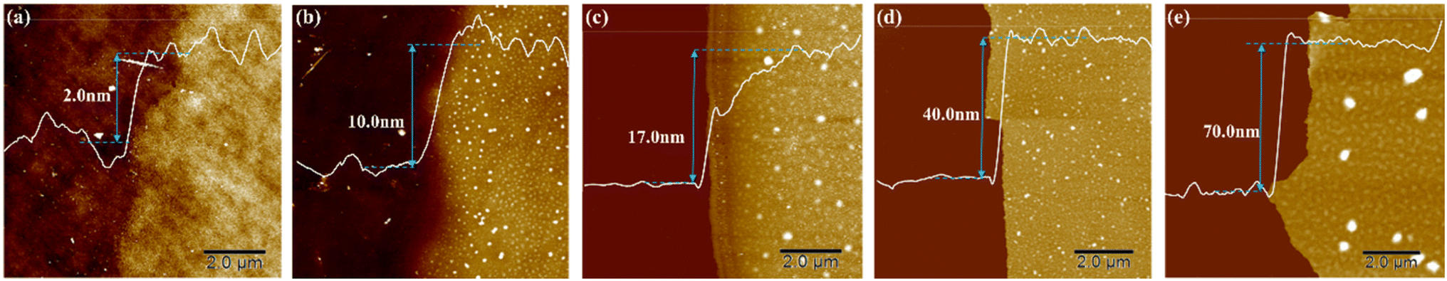 | ||
| Fig. 5 The surface topography and height profile of ex situ sulfurized Mo films (a) S1 sample, (b) S2 sample, (c) S3 sample, (d) S4 sample, (e) S5 sample. | ||
The cross-sectional images and crystalline structure of the S1 sample were analyzed using high-resolution transmission electron microscopy (HRTEM). In Fig. 6(a), continuous MoS2 films with 3–4 stacked layers are presented. The inset image of Fig. 6(a) shows a film thickness of 2.07 nm (with a monolayer thickness of approximately 0.69 nm), highlighting the structure and formation of a trilayer MoS2. These results are consistent with the AFM height analysis and Raman spectra findings. The crystalline structure of the S1 sample is depicted in Fig. 6(b), where the d-spacing of the 2H-MoS2 phase in the inset image is 0.27 nm, corresponding to the (100) plane. The selected area electron diffraction pattern in Fig. 6(b) includes the diffraction rings of the (100), (103), and (110) facets, indicating a polycrystalline structure for the S1 sample. Consequently, the crystalline structure of the film is characterized by the presence of grain boundaries and S vacancy defects.
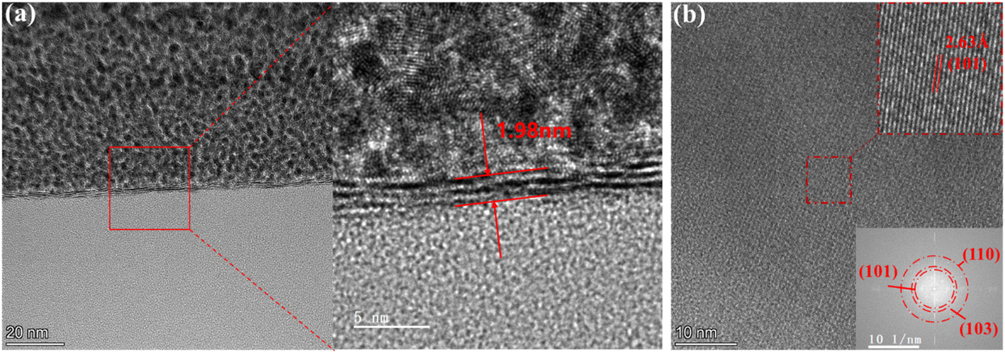 | ||
| Fig. 6 (a) Cross-sectional TEM images and (b) crystalline structure of S1 sample. | ||
To characterize the electrical transport properties of the ex situ sulfurized Mo film (S1), top-gated thin-film transistor (TFT) devices were fabricated using standard photolithography and etching processes, as illustrated in Fig. 7(a). As described in the experimental section, the trilayer MoS2 film grown on a 2-inch sapphire wafer was used as the semiconductor active layer for the top-gated TFT devices. The channel lengths (L) and widths (W) of the MoS2-based TFT devices are 10 μm and 20 μm, respectively. Ti/Au/Ti multilayers were employed for the source, drain, and gate electrodes, while a SiO2 layer served as the dielectric gate. Fig. 7(b) shows photographs of the FET array devices on a 2-inch sapphire wafer, including an amplified optical microscope image of a single TFT device. Although some devices in the marginal regions (the area within 2 mm of the wafer's edge) were non-functional, the majority in the middle region exhibited a well-defined structure, as depicted in Fig. 7(d).
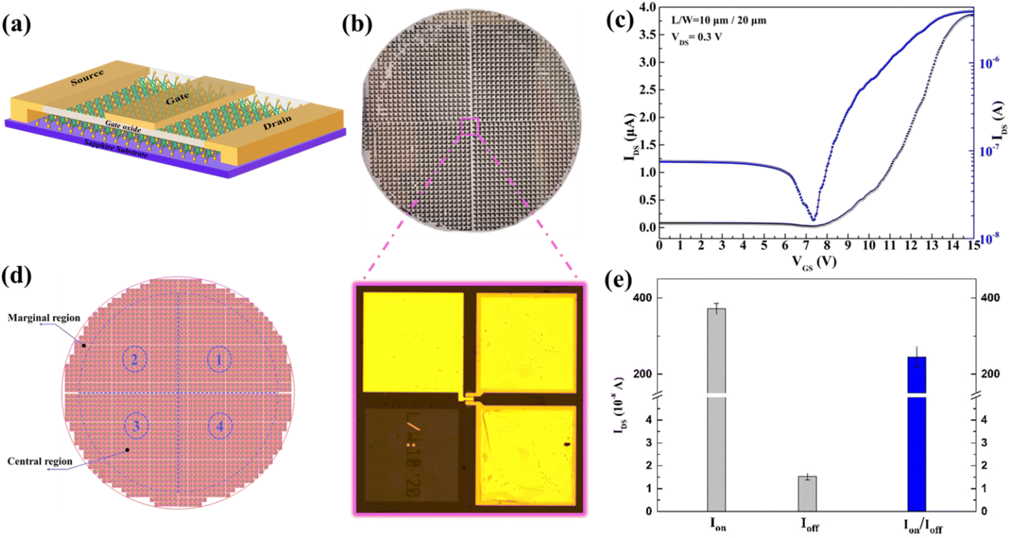 | ||
| Fig. 7 (a) Schematic diagram of the top-gated MoS2 TFT device; (b) the photographs of the TFT array devices integrated on a 2-inch sapphire wafer, and amplified optical microscope image of the single TFT device; (c) the typical transfer curves (IDS–VGS) of the trilayer MoS2-based TFT device; (d) schematic diagram of wafer device array; (e) statistical plot for the performances of 100 test devices. | ||
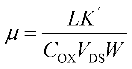
Fig. 7(c) shows the transfer curves of the MoS2-based TFT devices measured at a source-drain voltage of 0.3 V. The transfer curve shows that the trilayer MoS2 is a n-type semiconductor. The drain current (IDS) is shown by the blue curve, which is plotted on a logarithmic scale with respect to the gate voltage (VGS). At a VGS of 7.5 V, the MoS2 TFT channel exhibits an OFF-state current of approximately 1.6 × 10⁻⁸ A and an ON-state current of approximately 3.8 × 10⁻⁶ A at VGS of 14 V. The Ion/Ioff ratio of the TFT devices is about 2.3 × 10². The field effect mobility can be evaluated using the following formula:29
In total, 1768 thin-film transistors were fabricated on a 2-inch wafer. For the purposes of evaluation, 25 devices were selected at random from each central region, resulting in a total of 100 devices being tested. During the fabrication process, 27 devices were rendered inoperative due to the dislodgement of source, drain, or gate electrodes. Consequently, these devices were not suitable for standard electrical characterisation. Nevertheless, the remaining devices exhibited commendable TFT characteristics in their transfer attributes. However, the switching current was noticeably low, suggesting a need for further optimisation of the process to enhance device performance. The mean and standard deviation values of Ion, Ioff, and the ratio Ion/Ioff for the tested devices are depicted in Fig. 7(e).
The device performance of MoS2 TFT are influenced by several factors, including the intrinsic material properties, scattering effects, device architecture, and fabrication processes. Under controlled processing and testing conditions, however, the predominant factors affecting the electrical performance of these devices are the inherent material properties, such as crystal defects, impurities, layer count, and mechanical strain.4 The MoS2 used in these devices is typically polycrystalline, with well-defined grain boundaries and vacancies present within the thin film. These grain boundaries act as scattering centers for charge carriers, significantly impeding carrier mobility. Furthermore, the grain boundaries themselves can introduce localized electronic states that trap charge carriers, thereby reducing the material's overall conductivity. Sulfur vacancies within the lattice can also generate localized electronic states in the bandgap, which trap charge carriers and further degrade carrier mobility.15 Consequently, these factors contribute to a reduction in the electrical conductivity and overall performance of the transistor devices.
4. Conclusion
In conclusion, the TVS technique was employed both in situ and ex situ to synthesize wafer-scale 2D-MoS2 films. During the in situ heat treatment process, metal Mo films are oxidized to form the MoO2 phase, with only a minimal production of the MoS2 phase. In contrast, ex situ methods effectively inhibit the formation of the MoO2 phase, resulting in the pure polycrystalline MoS2 phase. Upon chemical and physical property characterization of the thin film post ex situ sulfidation, it was noted that the films can grow uniformly and continuously on a 2-inch wafer surface. By adjusting the thickness of the Mo film, a controlled transition from the bulk phase to few-layer MoS2 can be achieved. Electrical transfer measurements of the top-gate TFT devices reveal typical n-type semiconductor behavior for the trilayer MoS2, with a field effect mobility of 9.2 cm2 V−1 s−1 and an Ion/Ioff ratio of 2.3 × 10². These results show that the ex situ treatment approach can effectively produce high-quality 2-inch wafer-level 2D-MoS2, making it suitable for microelectromechanical fabrication processes and indicating a promising future for microelectronic devices based on 2D-MoS2 films.Data availability
The authors will supply the relevant data in response to reasonable requests.Conflicts of interest
There are no conflicts to declare.Acknowledgements
The authors acknowledge the financial support of this research by the Outstanding Youth Fund of Gansu Academy of Sciences 2024YQ-09, Longyuan Youth Innovation and Entrepreneurship Talent Project, Gansu province, Natural Science Foundation of Gansu Province (24JRRA1133, 24JRRA735), and the Youth Science and Technology Foundation of Gansu (22JR11RA206).References
- Y. Ren, Y. Niu, J. Jia, X. Cao and G. Zhang, Design and tribological performance of CrN/Mo2N/MoSx composite coating in wide temperature range inspired by oxidation kinetics principle, Tribol. Int., 2023, 180, 108299, DOI:10.1016/j.triboint.2023.108229.
- G. Anushya, M. Benjamin, R. Sarika, J. C. Pravin, R. Sridevi and D. Nirmal, A review on applications of molybdenum disulfide material: Recent developments, Micro Nanostruct., 2024, 186, 21, DOI:10.1016/j.micrna.2023.207742.
- Z. Ye, C. Tan, X. Huang, Y. Ouyang, L. Yang, Z. Wang and M. Dong, Emerging MoS2 Wafer-Scale Technique for Integrated Circuits, Nano-Micro Lett., 2023, 15(1), 38, DOI:10.1007/s40820-022-01010-4.
- C. Wang, Y. Song and H. Huang, Evolution Application of Two-Dimensional MoS2-Based Field-Effect Transistors, Nanomaterials, 2022, 12(18), 3233, DOI:10.3390/nano12183233.
- X. Liu, J. Chen, Y. Hu, Q. Pan, X. Du, H. Zhong, T. Zhang, C. Jiang, B. Ma and J. Chen, CVD growth of the centimeter-scale continuous 2D MoS2 film by modulating the release of Mo vapor with adjusting the particle size of Al2O3 microsphere, Chem. Phys. Lett., 2023, 813, 140292, DOI:10.1016/j.cplett.2022.140292.
- X. Xu, C. Zhang, M. K. Hota, Z. Liu, X. Zhang and H. N. Alshareef, Enhanced Quality of Wafer-Scale MoS2 Films by a Capping Layer Annealing Process, Adv. Funct. Mater., 2020, 30(11), 1908040, DOI:10.1002/adfm.201908040.
- D. Gupta, V. Chauhan and R. Kumar, Sputter deposition of 2D MoS2 thin films -A critical review from a surface and structural perspective, Inorg. Chem. Commun., 2022, 144, 109848, DOI:10.1016/j.inoche.2022.109848.
- Q. Wu, C. Wang, Q. Xu, X. Zhang, Z. Cai, L. Lin, X. Gu, K. Ostrikov, H. Nan and S. Xiao, Centimeter-level MoS2 films with controllable number of layers by face-to-face chemical vapor deposition strategy, Vacuum, 2023, 216, 112489, DOI:10.1016/j.vacuum.2023.112489.
- D. Tian, L. Kang, Z. Zhang, L. Meng, X.-a. Li and W. Yan, Controlled synthesis of continuous MoS2 films via space-confined vapor deposition, Chem. Phys., 2023, 571, 111923, DOI:10.1016/j.chemphys.2023.111923.
- M. S. Sirat, M. H. Johari, A. R. Mohmad, M. A. S. M. Haniff, M. H. Ani, M. I. Syono and M. A. Mohamed, Uniform growth of MoS2 films using ultra-low MoO3 precursor in one-step heating chemical vapor deposition, Thin Solid Films, 2022, 744, 139092, DOI:10.1016/j.tsf.2022.139092.
- D. Pradhan, S. P. Ghosh, A. Gartia, K. K. Sahoo, G. Bose and J. P. Kar, Modulation of microstructural and electrical properties of rapid thermally synthesized MoS2 thin films by the flow of H2 gas, Superlattices Microstruct., 2020, 145, 106598, DOI:10.1016/j.spmi.2020.106598.
- A. Shaji, K. Vegso, M. Sojkova, M. Hulman, P. Nadazdy, Y. Halahovets, L. Pribusova Slusna, T. Vojtekova, J. Hrda and M. Jergel, et al., Stepwise sulfurization of MoO3 to MoS2 thin films studied by real-time X-ray scattering, Appl. Surf. Sci., 2022, 606, 154772, DOI:10.1016/j.apsusc.2022.154772.
- T. Wang, J. Guo, Y. Zhang, W. Yang, X. Feng, J. Li and P. Yang, Synthesis of High-Quality Monolayer MoS2 via a CVD Upstream Deposition Strategy for Charge Capture and Collection, Cryst. Growth Des., 2024, 24(7), 2755–2763, DOI:10.1021/acs.cgd.3c01369.
- K. Hayashi, M. Kataoka, H. Jippo, J. Yamaguchi, M. Ohfuchi and S. Sato, Highly Sensitive NO2 Detection by TVS-Grown Multilayer MoS2 Films, ACS Omega, 2022, 7(2), 1851–1860, DOI:10.1021/acsomega.1c05113.
- R. Mathew and J. Ajayan, Material processing, performance and reliability of MoS2 field effect transistor (FET) technology- A critical review, Mater. Sci. Semicond. Process., 2023, 160, 107397, DOI:10.1016/j.mssp.2023.107397.
- A. Singh, M. Sharma and R. Singh, NaCl-Assisted CVD Growth of Large-Area High-Quality Trilayer MoS2 and the Role of the Concentration Boundary Layer, Cryst. Growth Des., 2021, 21(9), 4940–4946, DOI:10.1021/acs.cgd.1c00390.
- N. Choudhary, J. Park, J. Y. Hwang and W. Choi, Growth of Large Scale and Thickness-Modulated MoS2 Nanosheets, ACS Appl. Mater. Interfaces, 2014, 6, 21215–21222, DOI:10.1021/am506198b.
- J. Wei, F. Wang, B. Zhang, X. Shan, X. Di, Y. Li, Y. Feng and K. Zhang, High-performance FET arrays enabled by improved uniformity of wafer-scale MoS2 synthesized via thermal vapor sulfurization, Appl. Surf. Sci., 2019, 483, 1136–1141, DOI:10.1016/j.apsusc.2019.04.016.
- D. Mouloua, N. S. Rajput, J. F. Blach, M. Lejeune, M. El Marssi, M. A. El Khakani and M. Jouiad, Fabrication control of MoS2/MoO2 nanocomposite via chemical vapor deposition for optoelectronic applications, Mater. Sci. Eng., B, 2022, 286, 116035, DOI:10.1016/j.mseb.2022.116035.
- S. Feng, D. Li, H. Dong, S. Xie, Y. Miao, X. Zhang, B. Gao, P. K. Chu and X. Peng, Tailoring the Mo-N/Mo-O configuration in MoO2/Mo2N heterostructure for ampere-level current density hydrogen production, Appl. Catal., B, 2024, 342, 123451, DOI:10.1016/j.apcatb.2023.123451.
- A. Karataş and M. Yılmaz, Molybdenum disulfide thin films fabrication from multi-phase molybdenum oxide using magnetron sputtering and CVD systems together, Superlattices Microstruct., 2020, 143, 106555, DOI:10.1016/j.spmi.2020.106555.
- L. Wang, C.-Y. Bu, G.-H. Zhang, T. Jiang and K.-C. Chou, Preparation of MoO2 by the Solid State Reaction Between MoS2 and MoO3, Jom, 2015, 68(3), 1031–1036, DOI:10.1007/s11837-015-1681-4.
- H. Wang, J. Liu, Z. Wei, G. Hu, Z. Cui, Z. Zhao, Y. Zhang, F. Li, F. Gong and S. Wei, Engineering of Au nanoparticles over hollow MoS2/C nanoreactor for enhanced TEA sensing at low temperature, Vacuum, 2024, 224, 113114, DOI:10.1016/j.vacuum.2024.113114.
- M. Pramanik, B. Jana, A. Ghatak and K. Das, Improvement in efficiency of MoS2 nanoflower based ethylene gas sensor on transition metal doping: An experimental and theoretical investigation, Mater. Chem. Phys., 2024, 314, 128892, DOI:10.1016/j.matchemphys.2024.128892.
- J.-H. Choi, S.-W. Lee, H.-B. Kim and J.-H. Ahn, Effects of plasma conditions on sulfurization of MoO3 thin films and surface evolution for formation of MoS2 at low temperatures, Appl. Surf. Sci., 2020, 532, 147462, DOI:10.1016/j.apsusc.2020.147462.
- A. Hötger, W. Männer, T. Amit, D. Hernangómez-Pérez, T. Taniguchi, K. Watanabe, U. Wurstbauer, J. J. Finley, S. Refaely-Abramson, C. Kastl and A. W. Holleitner, Photovoltage and Photocurrent Absorption Spectra of Sulfur Vacancies Locally Patterned in Monolayer MoS2, Nano Lett., 2023, 23(24), 11655–11661, DOI:10.1021/acs.nanolett.3c03517.
- P. Yang, F. Liu, X. Li, J. Hu, F. Zhou, L. Zhu, Q. Chen, P. Gao and Y. Zhang, Highly Reproducible Epitaxial Growth of Wafer-Scale Single-Crystal Monolayer MoS2 on Sapphire, Small Methods, 2023, 7(7), 2300165, DOI:10.1002/smtd.202300165.
- Y. Jung, H. Ryu, H. Kim, D. Moon, J. Joo, S. C. Hong, J. Kim and G.-H. Lee, Nucleation and Growth of Monolayer MoS2 at Multisteps of MoO2 Crystals by Sulfurization, ACS Nano, 2023, 17(8), 7865–7871, DOI:10.1021/acsnano.3c01150.
- P. Yang, J. Zha, G. Gao, L. Zheng, H. Huang, Y. Xia, S. Xu, T. Xiong, Z. Zhang and Z. Yang, Growth of Tellurium Nanobelts on h-BN for p-type Transistors with Ultrahigh Hole Mobility, Nano-Micro Lett., 2022, 14, 11655–11661, DOI:10.1007/s40820-022-00852-2.
| This journal is © The Royal Society of Chemistry 2025 |