
 Open Access Article
 This Open Access Article is licensed under a
 Creative Commons Attribution 3.0 Unported Licence
Thermotransmittance spectroscopy of layered crystals using lab on fiber†
K.
Ciesiołkiewicz
 *,
J.
Kopaczek
and
R.
Kudrawiec
*
*,
J.
Kopaczek
and
R.
Kudrawiec
*
Department of Semiconductor Materials Engineering, Wroclaw University of Science and Technology, Wybrzeże Wyspiańskiego 27, 50-370 Wrocław, Poland. E-mail: karolina.ciesiolkiewicz@pwr.edu.pl; robert.kudrawiec@pwr.edu.pl
First published on 2nd July 2025
Abstract
Transition metal dichalcogenides are extensively studied for their unique optical properties, with emission and reflectance techniques commonly used to probe optical transitions. In this context, a thermotransmittance technique is introduced as a novel method to investigate the transmission and absorption properties of thin TMDC crystals transferred onto the core of multimode optical fibers. Using transmission and photomodulated transmission techniques, significant changes in the amount of transmitted light, reaching almost 60%, were detected. These changes, evoked by laser heating and subsequent heat accumulation, correspond to excitonic transitions. The obtained results indicate significant red shifts and changes in absorption coefficients around optical transitions, highlighting the materials’ sensitivity to temperature variations. As the laser illumination of the sample causes either an energy shift of optical transition or a change in the amount of transmitted light, these findings demonstrate that the TMDC-coated optical fibers could be utilized as light modulators or temperature sensors.
Introduction
The discovery of graphene in 2004 by scientists Andre Geim and Konstantin Novoselov at the University of Manchester1 marked the beginning of a new era in materials science and nanotechnology.2–4 Following the discovery of graphene, interest in other 2D materials soared, leading to the investigation of various materials with unique electronic,5 optical,6 and mechanical7 properties. Among layered materials, transition metal dichalcogenides (TMDCs) have emerged as up-and-coming candidates for a wide range of optoelectronic applications.8,9 Notable examples include molybdenum (Mo) and tungsten (W) combined with sulfur (S) or selenium (Se), which exhibit intriguing properties that make them attractive for technological advancements. TMDCs are characterized by strong covalent bonds within the layer and weak van der Waals bonds between adjoining layers, which makes them, like graphene, easy to isolate as monolayers through mechanical exfoliation.10 One of the most important features of TMDCs is their ability to transition from an indirect to a direct bandgap semiconductor when thinned down to monolayer form,11,12 while still strongly interacting with light.11 This transition has significant implications for their optoelectronic properties and potential applications.8,13,14 In particular, the spectral range for these materials typically falls between 1.55 to 2.00 eV,15 rendering them suitable for various optoelectronic devices.8,14 Furthermore, TMDCs exhibit compatibility with silicon substrates, facilitating their integration into existing semiconductor technologies.9,16 The mentioned properties, combined with their ease of manipulation and unique electronic structure,17 position TMDCs as promising candidates for the development of optoelectronic devices.18,19Another commonly used platform that is highly compatible with TMDC materials is optical fibers. These two scientific areas are increasingly being integrated.20 Optical fibers, renowned for their proficiency in light propagation, have limited use in applications such as photodetectors and sensors due to their material properties. However, integrating TMDC materials can overcome these limitations and enable new functionalities in optoelectronics.8,20 Moreover, fiber optics provide an excellent platform for light–matter coupling and, when integrated with 2D materials, allow the fabrication of compact and flexible optoelectronic devices.8,20–22 The popular ones are optical modulators,23,24 photodetectors25,26 and sensors.23,27,28
On the other hand, fiber optics, with their numerous advantages, can also be valuable for material characterization. One group of techniques widely used to study the optical properties of semiconductors is modulation spectroscopy, which, due to its differential nature, provides precise information about the optical transitions of the studied materials.29 Modulation spectroscopy, in its traditional approach, can be performed in both transmission and reflection modes,30 where internal parameters such as built-in electric field,31 strain,32 or temperature33 are slightly perturbed to obtain differential-like spectra with so-called resonances corresponding to optical transitions. Moreover, modulation techniques, alongside other commonly used optical methods such as PL, reflectance, or Raman spectroscopy, can be equally well employed to study material properties under the influence of various external factors, such as strain,34 temperature,35 and pressure,15,36 as well as magnetic fields,37,38 with each parameter varied across a broad range. These techniques provide detailed insights into the optical response of semiconductors and other materials. As mentioned, a commonly used approach to obtain modulation spectra is temperature perturbation (thermoreflectance), where the material is typically heated using a Peltier element39 or resistive heater.40 In addition, it has been shown that lasers can also be used to induce both significant and subtle changes in material properties.41–43
In this work, we propose a novel approach to lab-on-fiber measurements. Here, one of the methods that could benefit from combining it with optical fibers is optical transmission, based on which it is possible to estimate the absorption characteristics of studied materials.44 Furthermore, photomodulated transmission, a differential technique that allows obtaining information about direct optical transitions over a broad spectral range,45 could also be coupled with fibers. So far, these techniques have primarily been used to determine the fundamental band gap of semiconducting materials, as it is challenging to obtain a sample thin enough to allow light with energy higher than the band gap to transmit through due to stronger absorption.30 As mentioned, this phenomenon is related to the energy dependence of the absorption coefficient. Namely, a large increase in absorption is observed just above the bandgap and at higher energies, significantly reducing the initial intensity of light to a non-measurable level. Thinning down materials like van der Waals (vdW) crystals allows higher energy light to pass through and, therefore, to observe the transmission signal for this spectral range. In such a case, when analyzing the absorption spectra, optical transitions A and B (and even C) in TMDC crystals can be clearly observed, as shown in our studies. One of the approaches to the problems discussed above is the use of optical fibers in transmission measurements. Optical fiber, when light is introduced into its core, provides an attractive platform for creating micro-laboratories, known as lab-on-fiber (LOF).21,46 In our study, the standard surface of a flat optical fiber tip is 125 μm in diameter, and the core itself is 50 μm. Generally, obtaining a thin sample of these dimensions is not challenging. By covering the entire surface of the core with a thin layer of vdW crystals, the absorption of the light transmitted through it can be easily measured across a broad spectral range. Moreover, this approach allows for the measurement from a few layers down to even monolayers. Additionally, using fibers in optical measurements can simplify the experimental setup and enable the decoupling of the measurement zone from the sample location. So far, this approach, i.e., placing TMDCs on fiber, has been utilized once in optical measurements of WSe2 monolayer in a magnetic field.47 However, modulation spectroscopy techniques in such an experimental configuration have not been studied and reported.
Furthermore and most importantly, we demonstrate the use of an illuminating laser beam in transmission measurements to induce reversible changes in absorption spectra through controlled heating, thereby providing insight into the effects of temperature changes in the studied sample. All the measurements were conducted on the four most commonly studied TMD crystals, namely, MoS2, MoSe2, WS2, and WSe2, allowing us to focus on the thermal effects evoked by laser heating, as their optical properties are already well known. Each sample was measured at room temperature, with the power of the backlighting laser varying from 0 to 40 mW. The changes in the optical response, in terms of light absorbed by the studied material and induced by laser heating, were measured using a portable spectrometer. Moreover, modulation measurements, in which the laser light was periodically blocked and unblocked using a mechanical chopper, were employed. This approach subsequently allowed us to directly measure the effect of temperature variations on the intensity of transmitted light using the lock-in technique. We, therefore, propose a new thermotransmittance method that involves directly heating the sample using only a laser, eliminating the need for an additional heater. This approach allows precise local temperature control and uniquely enables these measurements to be performed in transmission mode using optical fibers.
Sample preparation and experimental setup
In this study, we employed a widely utilized multimode optical fiber characterized by a core dimension of 50 μm and a cladding of 125 μm, the selected for this study optical fibers operate in the spectral range of 400–2400 nm. To prepare the crystals for measurements, the mechanical exfoliation method was used, as it is known for its efficiency in obtaining thin layers of vdW materials.12 Through this method, it was possible to achieve the desired reduction in sample thickness in order to make them semitransparent for light. Following the preparation stage, samples with optimal dimensions to align with the core diameter of the fiber and reduced thickness, enabling light to transmit through the crystals and still be detectable, were selected. Once the appropriate samples were identified on PDMS, a transfer process was carried out under the microscope. In this case, we relied on the well-known deterministic transfer method, commonly used for placing crystals on desired substrates such as e.g., Si/SiO2.48 Establishing this approach in the context of optical fibers yields good results and demonstrates new possibilities. The materials were positioned onto the cleaved end-face of the optical fiber, a task that required precision to ensure proper alignment and adherence. The final alignment procedure was performed using a stage equipped with x–y–z adjustments controlled by micrometer screws.The optical fiber with the sample placed on it using the methodology described above was integrated into a transmission setup (Fig. 1). In this setup, a quartz tungsten halogen (QTH) lamp was used as the source of the probe beam, and the light transmitted through the sample was directly detected by a portable CCD spectrometer. On the other hand, conducting a modulated experiment requires adding the elements enclosed in the blue dotted frame to the setup. The continuous wave (CW) laser operating at 532 nm was used to induce changes in the internal parameters of the studied materials, thereby causing modulation of the transmitted light. Moreover, the lock-in technique was utilized to collect mentioned changes in the transmission spectra, which correspond to optical transitions. Both the light from the laser and the QTH lamp were precisely focused onto the end face of the optical fiber, with the sample on it, using a 20× micro-objective lens. The size of the laser spot focused on the sample is 10 μm in diameter (this value is above the diffraction limit and is attributed to the underfilling effect49,50). To ensure that the laser did not disturb the spectral range of interest, a 550 nm long-pass filter was implemented. The use of optical fiber in the experimental setup offered several significant advantages, including improved signal quality and flexibility in positioning the sample zone. Additionally, it allowed us to eliminate numerous optical components, such as mirrors and lenses, which are typically necessary to direct light in conventional setups without optical fibers. This simplified experimental arrangement and also reduced potential sources of alignment errors. Consequently, the optical fiber facilitated the direct guidance of the signal from the sample to the detector, thereby enhancing the efficiency of our measurements.
 | ||
| Fig. 1 (a) Schematic of the experimental setup for transmission measurements using an integrated optical fiber. Blue elements in dashed frames correspond to the configuration of the setup for modulated transmission. (b) Detailed view of the end face of the optical fiber, showing the measured sample. The bright orange circle represents the light transmitted through the sample. (c) Close-up schematic of the fiber tip, illustrating how the thin samples of the measured materials are positioned to cover the core of the optical fiber. The green and yellow cones represent the laser (pump beam, inducing changes in the transmitted light) and the light emitted from the halogen lamp (probe beam), respectively. | ||
Rapid optical transmission determination and thermal effects in TMDCs integrated with optical fiber
Firstly, transmission measurements on several well-known TMDC crystals using a spectrometer configuration (Fig. 1a) were conducted. The materials investigated included thin film (10–100 nm) of MoS2, MoSe2, WS2, and WSe2, which are semitransparent for light. In the absorption spectra shown in Fig. 2, we observed distinct excitonic transitions, exciton AK and exciton BK for MoS2 and MoSe2, and exciton AK for WS2 and WSe2. Observing these features indicates strong excitonic absorption within the studied materials and provides insight into their optical properties. For MoS2Fig. 2a, in the room temperature absorption spectra, the two measured features corresponding to the AK and BK excitonic transitions are located at approximately 1.843 eV and 2.003 eV, respectively. Similarly, MoSe2 exhibited A and B excitonic transitions but at lower energies, around 1.543 eV and 1.803 eV, Fig. 2b. All these transitions are characterized by a significant increase in absorption coefficient, highlighting the presence of strong excitonic absorption. The absorption spectra calculated from transmission measurements of WS2 and WSe2 (Fig. 2c and d) showed a single excitonic transition, the A exciton, at 1.958 eV for WS2 and 1.632 eV for WSe2. The absence of the B transition for tungsten-based crystals is related to a lower sensitivity of the experimental setup in this spectral range. All the energies of the excitonic transitions estimated from room temperature absorption spectra are summarized in Table 1. | ||
| Fig. 2 Absorption spectra of the MoS2 (a), MoSe2 (b), WS2 (c), and WSe2 (d) obtained with the increasing power of the backlight laser beam. The dependence of energy of excitonic transitions and the absorption coefficient at these energies on applied laser power is shown in the panel: (e) for MoS2, (f) for MoSe2, (g) for WS2, and (h) for WSe2. | ||
| Sample | Transition | E 0 (eV) | α (10−4 eV K−1) (ref. 51) | β (10−3 eV mW−1) | γ (K mW−1) |
|---|---|---|---|---|---|
| MoS2 | AK | 1.843 | 4.8 | 3.7 | 7.8 |
| BK | 2.003 | 6.2 | 3.8 | 6.1 | |
| MoSe2 | AK | 1.543 | 4.4 | 2.1 | 4.8 |
| BK | 1.803 | 5.7 | 3.1 | 5.4 | |
| WS2 | AK | 1.958 | 4.5 | 2.5 | 5.5 |
| WSe2 | AK | 1.632 | 4.4 | 3.4 | 7.7 |
To induce and study changes in optical response, specifically in the absorption coefficient, a laser beam was employed with incremental power steps tailored to each material: a 2 mW step for MoS2, WSe2, and WS2, and a finer 0.25 mW step for MoSe2. The laser beam illuminated the sample while transmission spectra were collected using a portable spectrometer, allowing the entire spectrum to be obtained at once after a set accumulation time. Throughout these measurements, a redshift in the energy of excitonic transitions for all studied materials was consistently observed, as shown in Fig. 2e–h. This redshift was attributed to the heating of the samples that were located at the tip of the optical fiber. In this case, the focused laser beam induces localized heating, leading to observed changes in the optical properties of the materials, referred to later in the text as the thermal effect. Despite the redshift of exciton energies with temperatures, a decrease in absorption coefficient at these energies was observed and is shown quantitatively in the bottom part of Fig. 2e–h. The changes in both energy and amplitude induced by heating the studied crystals were accompanied by spectral broadening of the optical transitions. To investigate this effect further, the linewidth of a selected TMDC sample (WSe2) was analyzed at different laser powers corresponding to increasingly higher temperatures. For example, at 0 mW, the linewidth was calculated to be 84 meV. At 10 mW, it increased to 107 meV, reaching a maximum value of 153 meV at 40 mW (which corresponds to ∼607 K). Fig. S2 of the ESI† presents the excitonic transitions with increasing broadening.
The mentioned thermal effect was observed because (i) the studied thin TMDC materials have a low heat capacity, resulting from the small volume of the crystals due to their low thickness, and (ii) poor thermal conductivity between the crystal and the optical fiber. In such a situation, when a laser illuminates material, the absorbed energy causes rapid and high temperature variations. This occurs since, as mentioned, limited thickness restricts heat conduction away from the spot where the laser illuminates the material. Moreover, the small area of the sample, which is only slightly larger than the diameter of the core of the optical fiber and laser beam, further limits lateral heat dissipation. These spatial constraints, specifically the small sample volume, result in high heat accumulation, significantly increasing the local temperature. Additionally, the optical fiber on which the TMDC thin layer is placed is made of glass, which has low thermal conductivity. This makes it less effective at drawing heat away from the vdW crystal. Consequently, the heat generated by the laser also remains within the TMDC layer rather than being conducted away through the glass substrate. In this case, the glass substrate acts more like an insulator, hindering the transfer of heat away from the material (a more detailed discussion on thermal effect is added in the ESI†). The maximum laser power reached in this study was 40 mW, corresponding to a temperature of 607 K, as estimated based on the energy shift of optical transitions and their temperature coefficients reported in previous studies.51 Above this threshold, sample degradation or thinning was observed. Importantly, within the 0–40 mW range, no damage is expected. Moreover, the observed degradation at 40 mW (∼607 K) is consistent with other studies reporting that temperatures exceeding 600 K are required to induce sample thinning.52 For these reasons, it can be concluded that the observed energy shift of excitonic transitions is primarily related to thermal effects.
For the purpose of quantifying the thermal effect on the exciton energy redshift shown in Fig. 2, a linear fit was used for each dependency. Table 1 shows the β coefficients representing the energy shift per 1 mW of laser power obtained from the linear fit for each optical transition and material. For example, for MoS2, the energy shift, i.e., β coefficient, is equal to 3.72 meV mW−1 for transition Ak and 3.8 meV mW−1 for transition Bk. These values highlight the pronounced responsiveness of the studied materials to changes in laser power. On the other hand, the temperature coefficient α, which describes the energy shift in TMDC materials with temperature, was determined in our previous studies.51 This allowed us to establish a direct relationship between laser power and the induced temperature changes, represented by the γ coefficient in Table 1. The performed analysis indicated that MoS2 is highly sensitive to both laser power and, at the same time, temperature fluctuations, as evidenced by the largest energy shift. Additionally, we observed that for MoS2 and WSe2, the changes in absorption spectra were most prominent, with optical features corresponding to excitonic transitions completely diminishing at the highest laser power.
The findings described above show that an optical fiber with a TMDC crystal placed on its tip could serve as either a light modulator or a sensor. For light modulation, it was demonstrated that the amount of transmitted light can be significantly reduced by simply illuminating the material with a laser. On the other hand, tracking the energy position could possibly allow for temperature determination. However, regardless of the application, it is crucial to calibrate such a device, as its optical response can vary slightly based on material composition or thickness.
Modulated transmission for optical transition analysis in TMDC crystals
Modulated transmission is one of the methods used to measure optical transitions of semiconductors. These transitions are represented in spectra by features that correspond to changes in absorption coefficient.45,53,54 Moreover, the mentioned changes are obtained with respect to the amount of light transmitted when the sample is not illuminated by the laser, i.e., the unperturbed absorption coefficient shown by the thick blue lines in Fig. 2a–d. The modulated measurements were performed at room temperature using the experimental system configuration, incorporating elements from the blue-dashed frame shown in Fig. 1. In this case, the spectrometer was replaced by a monochromator (Triax 320), to which an optical fiber was coupled. The dispersed signal from the monochromator was detected subsequently by a Si diode in the point-by-point mode. Furthermore, the signal, representing a change in the intensity of light transmitted through the sample, was measured using the lock-in technique with a reference signal from a mechanical chopper. Finally, the obtained results were compared with their simulated spectra obtained using (T − T0)/T formula, where T and T0 are transmission spectra collected with and without the backlight 532 nm laser beam, respectively. Notably, both T and T0 were collected across the entire spectral range at once using the portable spectrometer.Moreover, it is important to note that the shape of the spectra collected using the two approaches mentioned above will, in general, differ (compare, e.g., Fig. 3avs.3b). In the case of the method based on a portable spectrometer, the rapidly determined ΔT/T spectrum is also influenced by background signals across the entire energy range, which is not fully eliminated by normalization to a reference spectrum. In contrast, modulated transmission measurements rely on lock-in detection, where only the signal modulated at the chopper frequency (280 Hz in this case) is recorded. Furthermore, changes in the transmission spectrum appear only at energies corresponding to optical transitions. As a result, the background signal is suppressed, and the resonance appears centered around zero on the signal (y) axis, leading to a different spectral shape.
 | ||
| Fig. 3 Modulation spectra of four different transition metal dichalcogenides: MoS2 (a), MoSe2 (b), WS2 (c), and WSe2 (d) collected at different laser powers, and results of simulated modulation experiments performed for the MoS2 (e), MoSe2 (f), WS2 (g), and WSe2 (h) with the use of a spectrometer. The gray rectangular area represents the energy position of the A and B excitonic transitions obtained with low laser power. | ||
The results of the modulated experiment conducted with different laser powers for each of the studied crystals are shown in Fig. 3. As previously mentioned, the observed changes in the intensity of transmitted light in the spectra correspond to direct optical transitions. Here, these are the A and B excitonic transitions for Mo-based TMDCs and the A transition for W-based crystals. The energies of observed transitions agree well with the absorption spectra (Fig. 2) derived from measurements obtained using the first experimental configuration with a CCD spectrometer. It is also worth noting that the amplitude of the optical features/resonances is significant. Changes in the transmitted light for MoS2 are the largest, reaching up to 60% with a laser beam power of 40 mW, and even at 4 mW, they are around 20% at the energy of the A transitions. This was also observed in Fig. 2 for MoS2, where the reduction of the absorption coefficient at higher laser power was significant. In the modulation experiment, that change, i.e., between the amount of light transmitted at, e.g., 0 and 40 mW, was directly measured. Additionally, each optical transition is redshifted due to the increased laser power and stronger heating. These results demonstrate the high efficiency of the modulation method in directly determining changes in the intensity of transmitted light and observing optical transitions. Furthermore, the measurements revealed that, in addition to built-in electric field modulation, thermomodulation is the dominant factor in inducing changes in the transmission spectra (this aspect is discussed in the following section).
When comparing the two experimental methods, namely, modulation measurements and their simulated counterparts, it was concluded that the results and observed effects were highly consistent. However, for a quick assessment and determination of any changes in the material properties, the simulated approach using a spectrometer takes much less time, completing measurements within milliseconds. The only requirement is that the measured changes are at least on the order of around 0.3%. On the other hand, the modulation method, which utilizes the lock-in technique, is very sensitive, as modulated reflectance, detecting changes at the level of 10−5 to 10−6. However, collecting each spectrum requires more time, ranging from minutes to hours. Lastly and most importantly, the evoked changes are reversible within the applied laser power range, allowing for re-measurement and re-use of the fiber with the sample on it.
Effect of temperature and built-in electric field modulation on absorption
In order to separate the influences of internal electric field modulation and thermal effects induced by laser heating, comprehensive experiments were devised. This is because illuminating the studied crystal with a laser induces not only temperature changes but also modulates the internal built-in electric field in the semiconductor crystal. The presence of the built-in field arises from the difference in the Fermi level position at the surface compared to its energy location within the sample caused by surface states.55 As a result, when the laser shines on the sample and excites the electron–hole pairs, they are separated spatially by the internal electric field, causing a reduction in the strength of that built-in field. This is the basic principle of photoreflectance spectroscopy.30 Here, in the first experiment, two laser beams were directed onto the MoSe2 sample simultaneously: one with 1 mW power modulated by a mechanical chopper for direct determination of absorption changes using the lock-in technique and the second unmodulated backlight beam but with incrementally increased power for each separate measurement (from 0 to 16 mW with steps of 4 mW). The results of this experiment are presented in Fig. 4a, with the quantitative analysis included in Fig. 4d. It was revealed that the additional backlight (not modulated) beam is causing a redshift of optical transitions due to the laser heating. At higher backlight beam power (e.g., 16 mW), the amplitude of both transitions decreases because the energy provided by the modulated beam (1 mW), which induces changes in transmission, no longer causes significant temperature modulation compared to the constant temperature increase from the backlight beam. Furthermore, due to the photovoltaic effect, the reduction of the internal electric field would also lead to a smaller amplitude of optical transitions. However, such a large energy shift, as observed in Fig. 4d, is not expected in this case, suggesting that temperature modulation plays a more dominant role in evoking absorption changes. | ||
| Fig. 4 (a) Modulation spectra of MoSe2 crystal obtained in the configuration with an additional heating (backlight) laser beam. (b) Dependence of the spectra on the laser power of one modulated laser beam. (c) Modulation spectra obtained at different frequencies in the one-beam experiment. (d), (e) and (f) present the results of the analysis for the spectra included in panels (a), (b), and (c), respectively. | ||
Results of the second experiment, where only one beam, modulated by a mechanical chopper, was used to illuminate the sample, are shown in Fig. 4b. The presented spectra were collected with laser power steps of 3 mW. It can be seen that changes in the amount of transmitted light increase with the power of the laser beam, reaching around 12% for 30 mW. These changes occur at the energy of optical transitions, which redshift as a result of the thermal effect, as shown in the top panel of Fig. 4e. Moreover, the amplitude of these changes increases and then starts to saturate at around 15 mW (Fig. 4e, bottom panel). At this power, the rate of energy redshift also decreases. Such behavior may indicate that the maximum temperature variation is reached at a power of around 15 mW. Remarkably, even at relatively low powers, like 100 μW, significant changes are observed in the spectrum, including the amount of transmitted light and the redshift of the corresponding optical transitions. The observed changes in transmitted light at the energy of the optical transition in the experiment with 100 μW laser power reached approximately 3% (Fig. S5 in the ESI†). This proves the high sensitivity of the studied system, which consists of a TMDC crystal placed on top of the fiber tip. Furthermore, the applied range of low laser powers ensures the safety of the sample from potential damage due to overheating, making it invaluable for experimental and practical applications. It is also important to note that all of the observed changes were reversible.
Further studies focused on measurements with varying modulation frequencies in the one-beam experiment, the results of which are included in Fig. 4c and f. The spectra were collected with frequencies in the range of 80 to 480 Hz, while the power of the laser was set to 4 mW. It was shown that the observed changes in transmission do not shift spectrally, and the energy of the optical transitions remains nearly constant. This indicates that the average temperature of the sample is independent of the modulation frequencies, as shown schematically in Fig. S1 in the ESI.† Although the energy of the transitions remained constant, the signal amplitude started to decrease at 280 Hz following initial saturation (Fig. 4f, bottom panel). The decrease in signal amplitude can be caused by the decrease in the modulation amplitude of temperature and/or the modulation amplitude of the built-in electric field. In general, it can be expected that thermal processes are slower than electrical processes, which in this case are determined by the dynamics of occupation of defect states at the crystal surface/interface. To check this, photoreflectance measurements were performed for various frequencies for bulk MoSe2 crystals. In this experiment, the studied samples were millimeter-sized and placed on a copper holder using silver paint to minimize thermal effects. Similarly, the results obtained for the bulk crystal showed decreased signal intensity with frequency (Fig. S2†). Since temperature modulation can be excluded, the reduction in signal is attributed to changes in the modulation amplitude of the built-in electric field. This occurs because when the excited electron–hole pair is spatially separated by the internal electric field, causing its simultaneous reduction, one of the carriers moves toward the surface, where a trap state captures it. However, at higher frequencies, this trap state may not empty before the next laser pulse illuminates the sample due to time constraints, reducing signal intensity.56 That observation indicates that in addition to temperature modulation, internal electric field perturbation contributes to the measured changes in the intensity of transmitted light. The contributions of both effects cannot be easily quantified; nonetheless, it is expected that temperature modulation will become increasingly dominant at higher laser power. For these reasons – i.e., the unknown relative contributions of temperature modulation (the dominant component) versus built-in electric field modulation – it is difficult to predict the maximum modulation frequency at which the signal will remain detectable. This is especially true given that other factors, such as the quality of the interface between the fiber and the studied crystal or the volume of the crystal, can affect temperature modulation. However, based on the conducted experiment, it can be estimated that for a thin MoSe2 crystal, the maximum frequency at which it is still possible to distinguish the signal corresponding to optical transitions from background noise could reach around 800 Hz.
Line shape of thermotransmittance
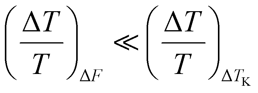
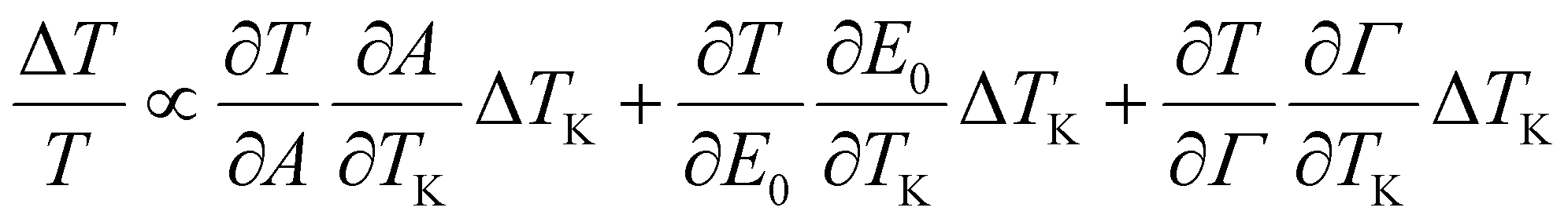
As discussed in the previous section, the influence of both the modulation of the internal electric field and the thermal effect induced by the laser are observed in the transmission spectra. The thermal effect resulting from localized heating of the material leads to changes in the absorption coefficients and other optical properties. These effects have a significantly stronger impact on the transmission spectrum compared to electric field modulation. As the laser power increases, the heat generated by the absorbed laser energy becomes the dominant factor driving changes in the optical characteristics of the studied materials, making the electric field modulation irrelevant at higher powers. The total contribution to the changes in the transmission spectrum can be described by the following equation: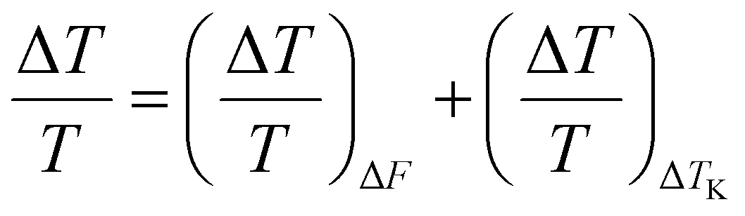 | (1) |
 | (2) |
The resonance profile (related to optical transition) follows a Lorentzian shape, characterized by three key parameters: the center energy E0 (corresponding to the energy measured without the laser), the resonance broadening Γ (peak half-width, FWHM), and the resonance strength A (oscillator strength)57,58(3):
 | (3) |
All these three parameters change due to the temperature variation induced by illuminating the studied sample with the laser beam. While Gaussian functions may better describe material inhomogeneities in some cases, Lorentzian fitting is commonly employed due to its simpler mathematical structure, which enables more efficient computation and faster convergence of fitting algorithms. For van der Waals crystals, which under ideal conditions exhibit high structural uniformity, Lorentzian fitting provides sufficiently accurate results while allowing effective analysis of experimental data.58 In the results, relative changes in transmission can also be described by the following equation:
 | (4) |
Below, in Fig. 5, the A optical transition measured for WS2 is presented. This excitonic transition was obtained from transmission measurements with a laser beam of 0 mW and 20 mW power illuminating the studied sample. The graph clearly shows how the spectrum shifts towards lower energies, broadens, and decreases in intensity as the laser power increases according to the expectation. Both of the obtained transitions were fitted with the Lorentzian function to quantify the changes induced by heating. The fitting highlights the gradual broadening of the resonance peak and the reduction in peak intensity, consistent with the expected thermal effects induced by laser heating. Differential signal has the resonance shape, which is approximated by the Aspnes formula:57
 | (5) |
 | ||
| Fig. 5 The optical transition of WS2 obtained from transmission measurements conducted with laser powers of 0 mW and 20 mW. The spectra exhibit a shift towards lower energies, broadening, and a decrease in amplitude with increasing laser power. The overlaid Lorentzian fitting (dashed lines) was applied to illustrate the changes in the transition shape. | ||
Summary
This study introduces a novel measurement technique, i.e., thermotransmittance spectroscopy of layered crystals, using a lab-on-fiber approach. Thin, semitransparent samples of MoS2, MoSe2, WS2, and WSe2 were prepared using mechanical exfoliation and deterministically transferred onto the fiber end-face. Subsequently, rapid transmission measurements, performed using a portable spectrometer, allowed for the extraction of absorption spectra while the studied samples were illuminated with increasingly higher laser power. Due to the low heat capacity of thin TMDC materials and poor thermal dissipation to glass optical fibers, the laser caused localized heating, leading to a significant temperature increase. This thermal effect resulted in the redshift of A and B excitonic transitions and a decrease in the absorption coefficient (reaching almost 60%) at energies corresponding to these transitions.The laser-induced changes in transmitted light were also directly measured using modulated transmission spectroscopy, employing different configurations and varying laser powers. The obtained results were compared with their simulated counterparts, both of which demonstrated significant changes in light transmission at energies corresponding to optical transitions. Furthermore, the laser power strongly affected the spectral position of these transitions, with the shift associated with thermal effects. Additionally, changes in transmitted light were primarily driven by temperature modulation, with a negligible contribution from internal electric field modulation, which is why the applied method is referred to as thermotransmittance. Moreover, in the studied material system, the sensitivity of the spectrometer measurements enabled the rapid determination of spectral shifts or changes in transmitted light intensity.
Overall, our comprehensive study demonstrated that TMDC crystals positioned on the core of an optical fiber tip could serve as temperature sensors or optical modulators. In the future, this system holds potential for further development in various applications, including measurements under external electric and magnetic fields, where the interaction between the magnetic field and excitonic transitions as a function of temperature could be explored. Lastly, it can expand the range of experimental conditions available for the study of TMDC materials.
Data availability
The data supporting this article are included in the ESI.† This includes a diagram illustrating temperature variations over time at two different modulation frequencies, as well as a figure presenting the photoreflectance spectra of MoSe2 obtained in the one-beam experiment.Conflicts of interest
The authors declare no conflicts of interest.Acknowledgements
This work was supported by project No. 2020/39/B/ST3/02704 (OPUS20) from the National Science Centre in Poland.References
- A. K. Geim and K. S. Novoselov, Nat. Mater., 2007, 6, 183–191 CrossRef CAS PubMed.
- R. Mas-Ballesté, C. Gómez-Navarro, J. Gómez-Herrero and F. Zamora, Nanoscale, 2011, 3, 20–30 RSC.
- S. Z. Butler, S. M. Hollen, L. Cao, Y. Cui, J. A. Gupta, H. R. Gutiérrez, T. F. Heinz, S. S. Hong, J. Huang, A. F. Ismach, E. Johnston-Halperin, M. Kuno, V. V. Plashnitsa, R. D. Robinson, R. S. Ruoff, S. Salahuddin, J. Shan, L. Shi, M. G. Spencer, M. Terrones, W. Windl and J. E. Goldberger, ACS Nano, 2013, 7, 2898–2926 CrossRef CAS PubMed.
- F. H. L. Koppens, T. Mueller, Ph. Avouris, A. C. Ferrari, M. S. Vitiello and M. Polini, Nat. Nanotechnol., 2014, 9, 780–793 CrossRef CAS PubMed.
- T. Dutta, N. Yadav, Y. Wu, G. J. Cheng, X. Liang, S. Ramakrishna, A. Sbai, R. Gupta, A. Mondal, Z. Hongyu and A. Yadav, Nano Mater. Sci., 2024, 6(1), 1–23 CrossRef CAS.
- G. Wang, A. Chernikov, M. M. Glazov, T. F. Heinz, X. Marie, T. Amand and B. Urbaszek, Rev. Mod. Phys., 2018, 90, 021001 CrossRef CAS.
- J. H. Kim, J. H. Jeong, N. Kim, R. Joshi and G.-H. Lee, J. Phys. D: Appl. Phys., 2019, 52, 083001 CrossRef.
- S. Yu, X. Wu, Y. Wang, X. Guo and L. Tong, Adv. Mater., 2017, 29, 1606128 CrossRef PubMed.
- J. Y. Lee, J.-H. Shin, G.-H. Lee and C.-H. Lee, Nanomaterials, 2016, 6, 193 CrossRef PubMed.
- R. Bian, C. Li, Q. Liu, G. Cao, Q. Fu, P. Meng, J. Zhou, F. Liu and Z. Liu, Natl. Sci. Rev., 2022, 9, nwab164 CrossRef CAS PubMed.
- E. M. Vogel and J. A. Robinson, MRS Bull., 2015, 40, 558–563 CrossRef CAS.
- M. Tamulewicz-Szwajkowska, S. J. Zelewski, J. Serafińczuk and R. Kudrawiec, AIP Adv., 2022, 12, 025328 Search PubMed.
- K. Thakar and S. Lodha, Mater. Res. Express, 2020, 7, 014002 CrossRef CAS.
- Electronics and optoelectronics of two-dimensional transition metal dichalcogenides | Nature Nanotechnology, https://www.nature.com/articles/nnano.2012.193, (accessed July 10, 2024).
- F. Dybała, M. P. Polak, J. Kopaczek, P. Scharoch, K. Wu, S. Tongay and R. Kudrawiec, Sci. Rep., 2016, 6, 26663 CrossRef PubMed.
- N. Youngblood and M. Li, Nanophotonics, 2017, 6, 1205–1218 CAS.
- A. Castellanos-Gomez, X. Duan, Z. Fei, H. R. Gutierrez, Y. Huang, X. Huang, J. Quereda, Q. Qian, E. Sutter and P. Sutter, Nat. Rev. Methods Primers, 2022, 2, 1–19 CrossRef.
- B. Sun, J. Xu, M. Zhang, L. He, H. Zhu, L. Chen, Q. Sun and D. W. Zhang, Crystals, 2018, 8, 252 CrossRef.
- H.-L. Liu, T. Yang, J.-H. Chen, H.-W. Chen, H. Guo, R. Saito, M.-Y. Li and L.-J. Li, Sci. Rep., 2020, 10, 15282 CrossRef CAS PubMed.
- Silica optical fiber integrated with two-dimensional materials: towards opto-electro-mechanical technology | Light: Science & Applications, https://www.nature.com/articles/s41377-021-00520-x, (accessed December 3, 2023).
- Y. Xiong and F. Xu, Adv. Photonics, 2020, 2, 064001 CAS.
- G. Kostovski, P. R. Stoddart and A. Mitchell, Adv. Mater., 2014, 26, 3798–3820 CrossRef CAS PubMed.
- H. Ahmad, H. S. Lim, M. Z. MatJafri, Y. Q. Ge, H. Zhang and Z. C. Tiu, Infrared Phys. Technol., 2019, 102, 103002 CrossRef CAS.
- J. Du, Q. Wang, G. Jiang, C. Xu, C. Zhao, Y. J. Xiang, Y. Chen and S. Wen, Sci. Rep., 2014, 4, 6346 CrossRef CAS PubMed.
- Y.-F. Xiong, J.-H. Chen, Y.-Q. Lu and F. Xu, Adv. Electron. Mater., 2019, 5, 1800562 CrossRef.
- J. Chen, Z. Liang, L. Yuan, C. Li, M. Chen, Y. Xia, X. Zhang, F. Xu and Y. Lu, Nanoscale, 2017, 9, 3424–3428 RSC.
- Y. Dogan and I. Erdogan, Opt. Quantum Electron., 2023, 55, 1066 CrossRef CAS.
- D. Hlushchenko, J. Olszewski, T. Martynkien, M. Łukomski, K. Gemza, P. Karasiński, M. Zięba, T. Baraniecki, Ł. Duda, A. Bachmatiuk, M. Guzik and R. Kudrawiec, ACS Appl. Mater. Interfaces, 2024, 16, 28874–28885 CrossRef CAS PubMed.
- M. Cardona, in Advances in Solid State Physics, ed. O. Madelung, Pergamon, 1970, pp. 125–173 Search PubMed.
- R. Kudrawiec and W. Walukiewicz, J. Appl. Phys., 2019, 126, 141102 CrossRef.
- J. Misiewicz and R. Kudrawiec, Opto-Electron. Rev., 2012, 20, 101–119 CAS.
- J. Kopaczek, R. Bartoszewicz, K. Ciesiołkiewicz, A. P. Herman, V. Mazánek, I. Plutnarova, Z. Sofer and R. Kudrawiec, ACS Appl. Electron. Mater., 2024, 6, 7857–7864 CrossRef CAS.
- C. H. Ho, S. L. Lin and C. C. Wu, Phys. Rev. B: Condens. Matter Mater. Phys., 2005, 72, 125313 CrossRef.
- Z. Li, Y. Lv, L. Ren, J. Li, L. Kong, Y. Zeng, Q. Tao, R. Wu, H. Ma, B. Zhao, D. Wang, W. Dang, K. Chen, L. Liao, X. Duan, X. Duan and Y. Liu, Nat. Commun., 2020, 11, 1151 CrossRef CAS PubMed.
- J. Kopaczek, M. K. Rajpalke, W. M. Linhart, T. S. Jones, M. J. Ashwin, R. Kudrawiec and T. D. Veal, Appl. Phys. Lett., 2014, 105, 112102 CrossRef.
- R. Oliva, M. Laurien, F. Dybala, J. Kopaczek, Y. Qin, S. Tongay, O. Rubel and R. Kudrawiec, npj 2D Mater. Appl., 2019, 3, 1–8 CrossRef CAS.
- A. A. Mitioglu, P. Plochocka, Á. Granados del Aguila, P. C. M. Christianen, G. Deligeorgis, S. Anghel, L. Kulyuk and D. K. Maude, Nano Lett., 2015, 15, 4387–4392 CrossRef CAS PubMed.
- K. Posmyk, N. Zawadzka, M. Dyksik, A. Surrente, D. Maude, T. Kazimierczuk, A. Babiński, M. Molas, W. Paritmongkol, M. Maczka, W. Tisdale, P. Plochocka and M. Baranowski, J. Phys. Chem. Lett., 2022, 13, 4463–4469 CrossRef CAS PubMed.
- D. Pierścińska, J. Phys. D: Appl. Phys., 2017, 51, 013001 CrossRef.
- A. M. Ślusarz, K. Komorowska, T. Baraniecki, S. J. Zelewski and R. Kudrawiec, ACS Sustainable Chem. Eng., 2022, 10, 8196–8205 CrossRef.
- Anisotropic Thermal Conductivity of Crystalline Layered SnSe2 | Nano Letters, https://pubs.acs.org/doi/10.1021/acs.nanolett.1c03018, (accessed November 18, 2024).
- J. Judek, A. P. Gertych, M. Świniarski, A. Łapińska, A. Dużyńska and M. Zdrojek, Sci. Rep., 2015, 5, 12422 CrossRef CAS PubMed.
- Temperature-Dependent Thermal Boundary Conductance of Monolayer MoS2 by Raman Thermometry | ACS Applied Materials & Interfaces, https://pubs.acs.org/doi/10.1021/acsami.7b11641, (accessed January 8, 2025).
- J. Kopaczek, F. Dybała, S. J. Zelewski, N. Sokołowski, W. Żuraw, K. M. McNicholas, R. H. El-Jaroudi, R. C. White, S. R. Bank and R. Kudrawiec, J. Phys. D: Appl. Phys., 2021, 55, 015107 CrossRef.
- F. Iikawa, A. A. Bernussi, A. G. Soares, F. O. Plentz, P. Motisuke and M. A. Sacilotti, J. Appl. Phys., 1994, 75, 3071–3074 CrossRef CAS.
- P. Vaiano, B. Carotenuto, M. Pisco, A. Ricciardi, G. Quero, M. Consales, A. Crescitelli, E. Esposito and A. Cusano, Laser Photonics Rev., 2016, 10, 922–961 CrossRef CAS.
- A. V. Stier, N. P. Wilson, G. Clark, X. Xu and S. A. Crooker, Nano Lett., 2016, 16, 7054–7060 CrossRef CAS PubMed.
- A. Castellanos-Gomez, M. Buscema, R. Molenaar, V. Singh, L. Janssen, H. S. J. van der Zant and G. A. Steele, 2D Mater., 2014, 1, 011002 CrossRef CAS.
- F. Helmchen and W. Denk, Nat. Methods, 2005, 2, 932–940 CrossRef CAS PubMed.
- L. Wawrezinieck, P.-F. Lenne, D. Marguet and H. Rigneault, in Biophotonics Micro- and Nano-Imaging, SPIE, 2004, vol. 5462, pp. 92–102 Search PubMed.
- J. Kopaczek, S. Zelewski, K. Yumigeta, R. Sailus, S. Tongay and R. Kudrawiec, J. Phys. Chem. C, 2022, 126, 5665–5674 CrossRef CAS PubMed.
- L. Hu, X. Shan, Y. Wu, J. Zhao and X. Lu, Sci. Rep., 2017, 7, 15538 CrossRef PubMed.
- K. Zelazna, M. Gladysiewicz, M. P. Polak, S. Almosni, A. Létoublon, C. Cornet, O. Durand, W. Walukiewicz and R. Kudrawiec, Sci. Rep., 2017, 7, 15703 CrossRef CAS PubMed.
- V. Karpus, B. Čechavičius, S. Tumėnas, S. Stanionytė, R. Butkute, M. Skapas and T. Paulauskas, J. Phys. D: Appl. Phys., 2021, 54, 504001 CrossRef CAS.
- M. Gladysiewicz, R. Kudrawiec, J. Misiewicz, G. Cywinski, M. Siekacz, P. Wolny and C. Skierbiszewski, Appl. Phys. Lett., 2011, 98, 231902 CrossRef.
- H. Shen, Z. Hang, S. H. Pan, F. H. Pollak and J. M. Woodall, Appl. Phys. Lett., 1988, 52, 2058–2060 CrossRef CAS.
- D. E. Aspnes, Surf. Sci., 1973, 37, 418–442 CrossRef CAS.
- J. N. Hilfiker and T. Tiwald, in Spectroscopic Ellipsometry for Photovoltaics: Volume 1: Fundamental Principles and Solar Cell Characterization, ed. H. Fujiwara and R. W. Collins, Springer International Publishing, Cham, 2018, pp. 115–153 Search PubMed.
Footnote |
| † Electronic supplementary information (ESI) available. See DOI: https://doi.org/10.1039/d5nr00301f |
| This journal is © The Royal Society of Chemistry 2025 |