
 Open Access Article
 This Open Access Article is licensed under a
 Creative Commons Attribution 3.0 Unported Licence
First principles investigation of hydrogen passivation for selective atomic layer deposition of Pt, Cu, and Au metals†
Giorgia
Barile
a,
Federico
Ravera
 *a,
Yuri
Ardesi
a,
Fabrizio
Mo
a,
Gianluca
Piccinini
a and
Mariagrazia
Graziano
b
*a,
Yuri
Ardesi
a,
Fabrizio
Mo
a,
Gianluca
Piccinini
a and
Mariagrazia
Graziano
b
aDept. of Electronics and Telecommunications, Politecnico di Torino, Corso Duca degli Abruzzi 24, Torino, Italy. E-mail: federico.ravera@polito.it
bDept. of Applied Science and Technology, Politecnico di Torino, Corso Duca degli Abruzzi 24, Torino, Italy
First published on 21st May 2025
Abstract
Atomic layer deposition (ALD) is a critical technique in nanofabrication, enabling precise thin-film deposition at the atomic scale. As devices become increasingly smaller and more complex, there is a critical need for deposition techniques that offer atomic-scale precision and spatial selectivity to design intricate patterns and structures. This study investigates the effects of hydrogen passivation on the deposition behaviour of platinum (Pt), copper (Cu), and gold (Au) using first-principles simulations. The density functional theory-based nudge elastic band method was employed to evaluate the energy barriers associated with the initial adsorption reactions of precursors on hydrogen-passivated and bare silicon substrates. Additionally, vibrational frequency calculations were performed to assess the thermodynamics of the reactions analyzed. Results showed that hydrogen passivation significantly increased the energy barriers for Pt, Cu, and Au, effectively hindering the deposition process on passivated surfaces. This passivation acts as a selective masking layer, suggesting favoured deposition on hydrogen-free regions. Gold exhibited the highest potential barrier difference among the metals studied, while platinum demonstrated the most controlled reaction pathways. Overall, the findings highlight the potential of hydrogen passivation in achieving selective ALD for advanced nanoscale device manufacturing.
1. Introduction & background
Atomic layer deposition (ALD) is a thin-film deposition technique that achieves atomic-level precision through self-limiting surface reactions by cyclically exposing the substrate to gaseous precursors. ALD has been successfully applied to deposit a wide variety of materials, resulting in precise, conformal thin films with excellent control over thickness and composition.1,2 Highly conformal oxides and semiconductors have been analyzed,3 and, although technologically challenging, conformal metal deposition is being studied as it is critical for electronic devices. Aluminium and palladium have been successfully deposited, with palladium being applied on substrates such as alumina, iridium, tungsten, and even polymers.4–8 Given the wide range of materials successfully deposited, ALD plays a vital role in semiconductor manufacturing,9–12 where precision and defect distribution directly influence the performance and functionality of electronic devices.One of the most recent applications of ALD is Area Selective ALD (AS-ALD),13 which was introduced to improve the selectivity and precision of the process, advancing nanofabrication and enabling precise atomic deposition.13,14 A key feature of AS-ALD is its selectivity, which allows thin films to be deposited only on specific surfaces or materials while preventing deposition on others. This selective capability is crucial for creating precise nanoscale patterns and features, particularly in electronic applications.15,16 AS-ALD achieves this by exploiting the chemical reactivity of chosen precursors with targeted surface regions, enabling deposition only on the desired areas of the substrate. AS-ALD has been applied in advanced semiconductor devices17 such as DRAMs18 and FinFET transistor gates14 and has been proposed to address novel nanoscale devices in the context of molecular Field-Coupled Nanocomputing technology.19,20 Beyond semiconductors, it addresses challenges like defect passivation and edge placement errors.21,22
Various approaches have been explored to achieve deposition selectivity in AS-ALD. Among these, self-assembled monolayers have been widely used to modify the chemical affinity between the substrate surface and the precursor. For example, n-alkyl-disulfides on gold surfaces enable precise surface patterning and manipulation,23 while octadecylphosphonic acid (ODPA) SAMs facilitate selective deposition on Cu, Co, W, and Ru.24 Plasma treatments have also been employed to enhance surface energy, improving precursor adhesion to polymeric surfaces.25 Selective nucleation techniques promote growth in specific areas of the substrate,26,27 and oxidized zones have been used to influence precursor adhesion, as seen in AS-ALD on functionalized graphene.28 Small molecule inhibitors have also been investigated to modify the chemical affinity between the substrate and the precursor.29 Other methods include altering substrate surface terminations with functional groups such as amino (NH2), phosphine (PH2), hydroxyl (OH), thiol (SH),30 or hydrogen,31 which act as masking agents. These alterations enable precise pattern formation by hindering deposition on specific areas.32 Hydrogen de-passivation has emerged as a promising technique to enhance the selectivity of ALD processes.31,33 By passivating the substrate with hydrogen and selectively removing it from specific areas of a silicon surface, the surface chemistry can be altered to favour selective deposition on hydrogen-free regions.34–36 This approach proved efficient for the selective deposition of HfO2,37 TiO2, and Al2O3,31,38,39 as confirmed either through experimental analysis or simulations.
Hydrogen de-passivation has the potential to enhance AS-ALD processes, which could significantly impact applications such as interconnections, contacts, and the development of new technological paradigms.20 However, the underlying mechanisms through which hydrogen de-passivation affects deposition behaviour, particularly for key industrial metals, remain poorly understood. Investigating these effects at the atomic scale is essential for optimizing ALD processes and unlocking their full potential in advanced applications. This study aims to bridge this gap by examining the thermodynamic and kinetic impacts of hydrogen passivation on metal deposition through first-principles simulations. More precisely, this research investigates its effects on the deposition of metals widely used in electronic applications:40–42
• Platinum (Pt) is widely used in electronic devices, offering reliable ALD deposition rates of approximately 0.45 Å per cycle at temperatures as low as 100 °C, with low impurity levels and roughness of 0.7 nm for a film thickness of 27 nm.43–45
• Copper (Cu), essential for metallization in the electronic industry, improves performance by reducing resistance and RC delay losses.46,47
• Gold (Au), with increasing attention in ALD,48–50 is used in various innovative applications, including sensors, photonics, and MEMS.51–53
This research employs nudge elastic band (NEB) calculations54 to investigate the deposition behaviour by evaluating the energy barriers of precursor reactions for Pt, Cu, and Au on both hydrogen-passivated and bare Si(100) substrates. Simulations provide insights into the reaction pathways of Pt, Cu, and Au precursors on both substrates. In particular, the focus is on the first adsorption step of the first precursor in the ALD cycle. The chosen precursors are trimethyl(methylcyclopentadienyl)platinum(IV) (MeCpPtMe3),44,45 copper(II) acetylacetonate (Cu(acac)2),55 and gold trimethyl(trimethylphosphine) (Me3AuPMe3).48 MeCpPtMe3 is widely adopted in ALD and has been used in various applications, including focused ion beam56 and sequential electron beam induced deposition (EBID).57,58 Cu(acac)2 is known for its stability and volatility, with deposited films exhibiting desirable characteristics, such as roughness of 10–20 nm on a 200 nm film deposited on Si substrates.59 Me3AuPMe3 has been successfully synthesized, and its deposition features have been studied, particularly on gold substrates.48,51,52,60 The results show an increase in potential barriers with the presence of the hydrogen passivation layer, indicating that passivation makes the first adsorption reaction in the initial cycle of the ALD process less energetically favourable. Therefore, these findings highlight the potential of hydrogen passivation as a masking layer to enable selective metal ALD, paving the way for further investigations into the complete ALD cycle.
2. Methodology
2.1 Computational methods
This work uses density functional theory (DFT)-level simulation within the ORCA61 framework62,63 to evaluate substrate selectivity. In particular, the analysis of the precursor reaction with the substrate is divided into two steps: geometry optimization (GO) to evaluate the stable geometries of involved compounds and nudge elastic band (NEB) simulations54 to investigate the reaction pathways.The GO and energy calculation parameters involve the Perdew–Burke–Ernzerhof (PBE)64 exchange–correlation functional and DEF2-TZVP as a basis set.65 Lastly, the D366,67 dispersion correction and GCP(DFT/TZ)68 counterpoise corrections were introduced to take into account van der Waals interactions and basis set superposition error.69–71
2.2 Simulated structure
Geometry optimizations were performed on the isolated precursors, the 2 × 4 Si(100)/H–Si(100) substrate clusters, and the initial and final states selected for the NEB calculations. The bottom layer of the simulated cluster is fixed and passivated with hydrogen to mimic bulk properties, while the reactive upper layer is left unconstrained for surface interactions. This choice guarantees consistent and comparable results among the simulations and optimizes computational resources. The geometry optimization provides the minimum energy of the initial state, whose value works as a reference for evaluating the energy pathways in the NEB simulations. The cluster model provides a well-established compromise between computational cost and accuracy for preliminary screening of surface reactivity in ALD contexts.72–74 Moreover, the cluster model can be adopted for comparative and qualitative analysis for AS-ALD, as previous works show.75–80 Future work will incorporate periodic slabs to validate current trends and better model the complete ALD process.2.3 Analysis of chemical reactions
The energy of the initial system, comprising the substrate and precursor, defines the reference energy state. From this state, the reaction pathway to the final state is determined through NEB simulations for all substrate−precursor combinations. Additionally, the adsorption energy for each combination is defined according to eqn (1):| Eads = Etot − Esub − Eprec | (1) |
The chemical reactions involved were selected based on the results of the literature, each justified in its respective section. The NEB calculations investigate the energetic transition state for the reactions involved. Comparing the transition state energies permits preliminary evaluations of the selectivity of the ALD process achieved through H terminations.
To complement our analysis, we computed the projected density of states (PDOS) and electron density distributions before and after adsorption on Si(100) and H–Si(100) surfaces. Although the finite cluster model lacks the full periodicity of a bulk substrate, it captures key local precursor–surface interactions and offers initial insights into the electronic interaction mechanisms underlying the early ALD steps, thus providing a basis for more detailed investigations. Additionally, we also calculated the Mulliken population in the initial and final states of each reaction to preliminarily evaluate charge transfer mechanisms. Calculations were performed with QuantumATK 2024.0981,82 using FHI pseudopotentials, the DZDP basis set, the PBE + D3 functional, a [4, 4, 4] Å−1k-point density, and a 100 Hartree mesh cutoff. PDOS was evaluated over −5 eV to +5 eV with 3001 points and a 12 × 12 Å−1 Monkhorst–Pack grid. Dirichlet boundaries and sufficient vacuum ensured proper electrostatic convergence.
2.4 Temperature effect evaluation
To further assess the process selectivity and the reaction spontaneity under analysis, we also present the Gibbs free energy difference results, calculated using eqn (2):| ΔG = ΔH − ΔTS | (2) |
In the Gibbs free energy analysis, three different temperatures were considered to provide a reference temperature range for future experimental validations. Specifically, this work studies the temperatures 273.15 K, 298.15 K, and 373.15 K. This approach yields insights into the stability and selectivity of the first adsorption in the chosen ALD processes for Pt, Cu, and Au on various substrate configurations and the effectiveness of passivation.
3. Results
This section presents the reaction pathways explored in this study. We analyzed two configurations for the three metals: bare silicon and hydrogen-terminated silicon. Additionally, we investigate a supplementary case for Au deposition on the passivated substrate by constructing two distinct reaction pathways. The investigation focuses on evaluating the reaction energy curves to assess the effectiveness of the passivation process by comparing the energy barriers associated with each reaction. The results are organized by metal type, with adsorption reactions analyzed for each metal and the extracted data scrutinized for insights. Finally, we comprehensively compare the results to determine which metal exhibits the highest susceptibility to passivation.3.1 Reaction pathway analysis of Pt deposition
Two reaction pathways were examined to describe Pt deposition: one involving the hydrogen-terminated substrate and one associated with the dangling bond (DB) configuration. Eqn (3), also referred to as reaction A, states the reaction between the Si(100) and MeCpPtMe3.44,45| Si + MeCpPtMe3 → Si–MeCpPtMe2–CH3 | (3) |
Conversely, eqn (4), hereafter labelled reaction B, displays the H–Si(100)-MeCpPtMe3 reaction.
| (Si–H) + MeCpPtMe3 → (Si–H)–MeCpPtMe2 + CH4 | (4) |
In both cases, a ligand-exchange reaction between the precursor and the substrate surface is considered.1Fig. 1(a) shows the Si(100)-MeCpPtMe3 reaction. In the final configuration, the precursor binds to the substrate by breaking one of its Me3–Pt bonds. Fig. 1(c) instead portrays the reaction pathway from the initial to the final configurations, highlighting the transition state (TS) found during the simulation. The initial configuration is very stable, and the reaction presents a potential barrier of 0.45 eV. However, the reaction pathway curve significantly drops at reaction coordinate 7, indicating slight reactivity issues in the configuration counteracted by the presence of the potential barrier. Similarly, Fig. 1(b) shows the structures for the reaction on H–Si(100).
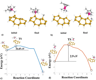 | ||
| Fig. 1 Geometrical structures for the platinum NEB simulations; (a) the initial and final configurations for reaction A. (b) The initial and final configurations for reaction B. (c) Reaction pathway obtained for reaction A. (d) Reaction pathway for reaction B, highlighting the respective TS configuration and location. | ||
A Me3–Pt bond breaks and gathers one H atom detached from the Si substrate, producing CH4 as a byproduct. Fig. 1(d) highlights the reaction pathway for the passivated substrate reaction. It conveys a higher energy barrier of 2.90 eV in the reaction pathway, indicating the effectiveness of the passivation as an inhibitor of the reaction. Fig. 2 shows the comparison in energy for each reaction coordinate in the two cases under analysis. Hydrogen passivation effectively increases the energy barrier, enhancing the selectivity of the Pt first adsorption.
 | ||
| Fig. 2 MeCpPtMe3 reaction pathways. Reaction A pathway is in blue, reaction B is in red; the difference in barrier height is relevant and suggests deposition selectivity of the process. | ||
Further calculations were computed to provide a more complete picture of the reactions. First, the adsorption energy is evaluated to give insight into the energetic state of the reactions. Reaction A has an adsorption energy of about −2.87 eV and reaction B of −1.86 eV. The lower adsorption energy in the Si(100)-MeCpPtMe3 case further entails that the MeCpPtMe3 is more likely to bind to the bare silicon, and the hydrogen passivation successfully hinders the adsorption reaction. Secondly, Fig. 1 in the ESI† shows the PDOS analysis. Panel (a) highlights the change in Pt d-orbitals between the initial and post-bonding stages of reaction A, with broadened and merged peaks and a reduced HOMO–LUMO gap, indicating orbital hybridization. After adsorption, the dxy and dxz orbitals show increased occupation below the Fermi level (EF) compared to the other contributions, thus suggesting a favoured direction of the Pt–Si bond. Similarly, panel (b) for reaction B indicates orbital hybridization and directional Pt–Si bond. We computed the Mulliken population to assess charge transfer during the reactions, with results presented in Table 2 in the ESI.† Reaction A shows a negligible initial charge transfer, indicating no significant interaction. In the final state, charge redistribution (+0.1053e and −0.1053e) confirms a precursor-to-substrate electron transfer. Similarly, reaction B also exhibits modest redistribution in the final state (+0.0131e and −0.0131e), suggesting weak precursor–substrate interaction, possibly limited by Si atom saturation with hydrogen. Future work will consider periodic bulk models that better represent the extended substrate to capture charge transfer mechanisms with more accuracy. Additionally, Fig. 2(a) and (b) in the ESI† display electron density plots, showing bond formation between Pt and the substrate for reactions A and B, respectively.
Finally, as per the temperature effect evaluation, calculations are provided to compute Gibbs Free energy variation. Concerning reaction A, the variation in entropy between the final and initial configurations at ambient temperature amounts to ΔTS = −0.5588 kcal mol−1, as per the enthalpy, ΔH = −54.6002 kcal mol−1, resulting in a Gibbs free energy variation of −54.0415 kcal mol−1. On the other hand, for reaction B, ΔTS = 3.5596 kcal mol−1 and ΔH = −34.2928 kcal mol−1, amounting to ΔG = −37.8523 kcal mol−1. Therefore, for reaction A, the Gibbs free energy is negative, with both entropy and enthalpy changes being negative. This indicates that the reaction is endothermic and spontaneous only at low temperatures. In contrast, reaction B, which has a positive entropy change, is spontaneous at all temperatures. However, at ambient temperature, reaction A exhibits a more negative Gibbs free energy compared to reaction B. These considerations further confirm that the adsorption reaction happens more easily with the DB substrate, endorsing the results and the considerations made for the portrayed energy pathways.
The Gibbs energy analysis is extended to include data evaluated at other temperatures, whose entropy, enthalpy, and Gibbs free energy differences results are reported in Table 1. For clarity, the last column in Table 1 states the spontaneity of the reaction at hand. Detailed intermediate data from the Gibbs analysis can be found in Table 1 of the ESI.†
| ΔTS [kcal mol−1] | ΔH [kcal mol−1] | ΔG = ΔH − ΔTS | |||
|---|---|---|---|---|---|
| MeCpPtMe3 273.15 K | A | −0.3573 | −54.6184 | −54.2612 | Spontaneous at low T |
| B | 2.1293 | −34.9837 | −37.1130 | Spontaneous at all T | |
| MeCpPtMe3 298.15 K | A | −0.5588 | −54.6002 | −54.0415 | Spontaneous at low T |
| B | 3.5596 | −34.2928 | −37.8523 | Spontaneous at all T | |
| MeCpPtMe3 273.15 K | A | −0.6992 | −54.8092 | −54.1100 | Spontaneous at low T |
| B | 2.8143 | −34.8312 | −37.6454 | Spontaneous at all T |
The additional simulations in Table 1 were conducted at 273.15 K and 373.15 K. The data confirm the conclusions drawn from the ambient temperature analysis and reveal that 373.15 K is not high enough to render reaction A non-spontaneous. As Pt ALD typically operates within this temperature range, the results indicate that reaction A remains spontaneous and is more favourable than reaction B under typical ALD conditions.
3.2 Reaction pathway analysis of Cu deposition
This section analyses copper deposition by using copper(II) acetylacetonate55 (Cu(acac)2) as the precursor. Similarly to Pt, the analysis includes its reaction with the DB and the H-terminated Si(100). The first reported reaction is shown in eqn (5), also referred to as reaction C. Fig. 3(a) shows the reaction between bare silicon and Cu(acac)2.| Si + Cu(acac)2 → Si–C5H8O2Cu(acac) | (5) |
 | ||
| Fig. 3 (a) Initial and final configurations for reaction C; (b) initial and final configurations for reaction D; (c) detailed pathway progression for reaction C; (d) reaction pathway for reaction D, both highlighting the TS and the respective potential barrier height. | ||
Specifically, a ligand exchange between one of the precursors Cu–O and a DB on the silicon substrate was assumed, permitting precursor adsorption.
Eqn (6) shows the H–Si(100)–Cu(acac)2 reaction, also labelled as reaction D, graphically depicted in Fig. 3(b). In this case, one of the Cu–O bonds breaks to gather one of the H atoms to achieve an acetylacetone-like configuration.
| (Si–H) + Cu(acac)2 → (Si–H)–(OH)C5H8OCu(acac) | (6) |
Fig. 3(c) illustrates the energy pathway for the Si(100) case. The curve shows a slight rise corresponding to the TS, located just before a significant energy drop. Moreover, the TS at reaction coordinate five is immediately followed by a steep energy decline beginning at reaction coordinate 7. The drastic drop indicates the instability of the TS configuration, and the curve shows a modest 0.03 eV potential barrier. Moreover, the final state being the most energetically stable, the reaction appears to be effectively unavoidable. Fig. 3(d) shows the energy curve for reaction D. The energy pathway presents a dome-like shape, with the final state being more energetically favourable than the initial state. Hydrogen passivation effectively increases the energy barrier to 1.22 eV, enhancing the selectivity of the copper deposition process. With respect to the system geometry at the transition state, in Fig. 3(c), the system at the TS shows the precursor hovering over the substrate, and the adsorption occurs after the drop in the reaction pathway. On the other hand, the system geometry at the TS in Fig. 3(d) shows a configuration with Cu(acac)2 already adsorbed onto the Si(100).
Finally, Fig. 4 shows the comparison between the geometrical structure of the initial and final configuration described above and the respective reaction pathway curves. The increase in the TS for reaction D is evident.
 | ||
| Fig. 4 Reaction pathways analyzed for the copper precursor deposition. The blue line represents the data obtained from the simulation of reaction C; the red curve refers to reaction D. The increase in barrier height and the dome-like shape assumed by the red line are evident. | ||
The computed Eads values are −2.15 eV for reaction C and −0.58 eV for reaction D. Therefore, the reaction with the bare Si(100) provides a more stable system configuration. The PDOS for the Cu precursor is shown in Fig. 1(c) and (d) in the ESI† for reactions C and D. The PDOS evolution is similar to the Pt case, with additional hybrid states near the Fermi level, though bonding with bare Si(100) is less directional. For H–Si(100), Cu d-orbitals show more Lorentzian-like features, indicating less hybridization.
PDOS evolution is similar to the Pt case, with additional hybrid states near the Fermi level, although bonding with bare Si(100) is less directional. For H–Si(100), Cu d-orbitals show more Lorentzian-like features, indicating less hybridization.
In reactions C and D, the final states exhibit a distinct charge transfer from the precursor to the substrate, as shown in Table 2 of the ESI,† indicating moderate electron redistribution upon adsorption. Fig. 2(c) and (d) of the ESI† show electron density visualizations, indicating bond formation in both reactions. The Gibbs free energies provide valuable insights into the thermodynamics of these reactions, and the results are summarized in Table 2. At ambient temperature, the calculated values of ΔTS = 1.0401 kcal mol−1 and ΔH = −39.5645 kcal mol−1 result in ΔG = −40.6046 kcal mol−1 for reaction C. The negative Gibbs free energy suggests that the reaction is endothermic and spontaneous at all temperatures. Moreover, reaction D shows ΔTS = 3.0650 kcal mol−1 and ΔH = 0.6275 kcal mol−1, which yield a barely negative ΔG = −2.4375 kcal mol−1. The positive value for enthalpy indicates that this reaction is spontaneous only at high T. Consequently, the surface passivation effectively prevents the initial adsorption required in the ALD process under consideration. The Gibbs free energy data for the other temperature consistently yield the same results: C is spontaneous at all temperatures and D is spontaneous at high temperatures. The increase in temperature does not drastically change the data. Therefore, considering reaction C Gibbs energy difference has a higher absolute value, the preferential adsorption previously highlighted still holds. Detailed and intermediate data for all reaction steps are provided in Table 1 of the ESI.†
| ΔTS [kcal mol−1] | ΔH [kcal mol−1] | ΔG = ΔH − ΔTS | |||
|---|---|---|---|---|---|
| Cu(acac)2 273.15 K | C | 0.9004 | −39.6493 | −40.5498 | Spontaneous at all T |
| D | 2.7841 | 0.5628 | −2.2213 | Spontaneous at high T | |
| Cu(acac)2 298.15 K | C | 1.0401 | −39.5645 | −40.6046 | Spontaneous at all T |
| D | 3.0650 | 0.6275 | −2.4375 | Spontaneous at high T | |
| Cu(acac)2 373.15 K | C | 1.4858 | −39.3246 | −40.8105 | Spontaneous at all T |
| D | 3.9264 | 0.8438 | −3.0826 | Spontaneous at high T |
3.3 Reaction pathway analysis of Au deposition
Three primary reaction pathways are examined for Au deposition: two involving the hydrogen-terminated substrate and one associated with the DB configuration. For the simulation, Me3AuPMe3 has been selected as the precursor, given its favourable chemical properties, stability, and consistent performance in Au-on-Au ALD processes.48 Experimentally, this precursor demonstrates a steady growth rate of (0.030 ± 0.002) nm per cycle on gold seed layers, high purity even at low deposition temperatures, and resistivity of 5.9 ± 0.3 μΩ cm, advantageous for conductive layer formation.51,52,60Eqn (7), hereafter referred to as reaction E, reports the reaction between the bare Si(100) and Me3AuPMe3. The precursor binds to the surface, losing a methyl group, which adsorbs on the Si(100) substrate. Fig. 5(a) graphically shows the analysed reaction.| Si + Me3AuPMe3 → Si–Me2AuPMe3–CH3 | (7) |
 | ||
| Fig. 5 Geometrical structures (images) output from the NEB simulations; (a) initial and final configurations for reaction E; (b) initial and final configurations for reaction F; (c) initial and final configurations for reaction G; (d) reaction pathway output for reaction E highlighting the lack of TS and potential barrier; (e) reaction pathway, potential barrier and TS for reaction F; (f) reaction pathway, barrier height and TS for reaction G. | ||
The reaction between the hydrogen-passivated substrate and Me3AuPMe3 was investigated in two different mechanisms. The first reported in Fig. 5(b), and described in eqn (8) (reaction F), involves CH3 detachment and CH4 formation as a byproduct. The methyl group binds with the H atom removed from the substrate surface, and the now-exposed Si atom subsequently binds with the Au atom of the precursor.
Fig. 5(c) and eqn (9) (reaction G) describe the second reaction mechanism considered. In this case, the precursor molecule unbinds Me3P, producing Me3PH (trimethylphosphine) as a byproduct. Thus, the precursor breaks apart, with the gold atom binding to the substrate, while the freed H atom bonds with phosphorus.
| (Si–H) + Me3AuPMe3 → (Si–H)–Me2AuPMe3 + CH4 | (8) |
| (Si–H) + Me3AuPMe3 → (Si–H)–Me3Au + PMe3–H | (9) |
Both configurations are of interest for this work. Indeed, it is typical for CH4 to be released as a byproduct in ALD reactions with precursors presenting methyl groups.83,84 As per reaction G, the formation of trimethyl phosphine is an assumed behaviour in light of the reaction found in the literature for Au-on-Au ALD.52
The reaction involving the stripped substrate shows significant reactivity issues since the precursor prematurely attaches to the substrate. Hence, during geometry optimization, it was necessary to constrain the precursor to manage the high reactivity of the molecule and provide a suitable and convergent result. The energy profile shown in Fig. 5(d) illustrates a lack of a potential barrier. In this case, the TS does not correspond to an energy maximum but rather aligns with a saddle point along the pathway. The adsorption itself occurs toward the end of the reaction. Although this instability typically poses challenges, it actually benefits this study. Indeed, the reaction proceeds unavoidably; any additional barrier would inhibit the process, thus suggesting the potential for atomic-scale pattern formation. Hydrogen passivation, in contrast, significantly raises the energy barrier. A detailed view of the isolated energy curves and their corresponding TS for reactions F and G can be found in Fig. 5(e) and (f), respectively. The passivation proves highly effective in preventing precursor adsorption. The energy profile for reaction F also shows a lower final energy, indicating a more stable configuration. Overall, the hydrogen-passivated substrate exhibits higher energy barriers than the un-passivated one, highlighting the potential masking effect of the hydrogen layer in the deposition process.
Fig. 6 shows the energy pathways for all the reactions considered. In detail, the yellow, blue, and red curves represent the energy pathways for the reactions E, F, and G, respectively. The comparison makes it possible to appreciate the increase in energy barrier for reactions F and G. More precisely, the increase in eV for reaction F amounts to 1.79 eV, and 1.58 eV for reaction G.
 | ||
| Fig. 6 Au reaction pathways highlighting the absence of a potential barrier for reaction E of Me3AuPMe3 with bare silicon, and the comparable barrier height increase of reactions G and F for the adsorption of Me3AuPMe3 onto the hydrogen passivated substrate. The yellow curve represents reaction E, the red curve represents reaction G, and the blue curve represents reaction F. | ||
As per the previously analyzed reactions, adsorption energy and Gibbs free energy variations were evaluated, with the adsorption energy values as follows: 5.15 eV for reaction E, 7.05 eV for reaction F, and 9.06 eV for reaction G, suggesting the reaction with the Si(100) dangling bonds is more stable and more probable. Reactions F and G show less spontaneity compared to the DB case, reinforcing the effectiveness of H passivation in achieving the necessary inhibition. Fig. 1(e) in the ESI† suggests a weak, nondirectional Au–Si(100) bond, with a minimal d-orbital contribution to chemical bonding. The Au d-orbital occupation changes little upon hydrogenation for both reactions F and G, showing limited hybridization (Fig. 1(f) and (g) in the ESI†). The absence of significant changes in the d-orbital populations indicates weak interactions and limited electronic coupling at the interface. The results of the Mulliken analysis are reported in Table 2 in the ESI† for reactions E, F, and G. The final states suggest electron transfer from the precursor to the substrate. Notably, reactions F and G exhibit relatively large charge variations despite minimal involvement of the Au d-orbitals. Future work should further validate these findings, ideally supported by experimental data. Furthermore, the electron density analysis in Fig. 2(e–g) in the ESI† suggests the presence of shared electrons between Au and Si for all the reactions. Table 3 reports the relevant data for Gibbs free energy calculation. Extended and intermediate data for all the steps of the reaction can be found in Table 1 in the ESI.† At ambient temperature, the calculation reveals for reaction E ΔG = −102.6577 kcal mol−1, ΔTS = 9.4926 kcal mol−1, and ΔH = −93.1651 kcal mol−1, making it endothermic and spontaneous at all temperatures. For reaction F, ΔG = −32.1031 kcal mol−1, ΔTS = 3.0557 kcal mol−1, and ΔH = −29.0474 kcal mol−1, indicating it as spontaneous at all temperatures but slower than reaction E. Reaction G, with ΔG = 14.3649 kcal mol−1, ΔTS = 1.2614 kcal mol−1, and ΔH = 15.6262 kcal mol−1, has a positive Gibbs free energy variation and enthalpy, making it spontaneous only at high temperature. The extended temperature analysis remains consistent with the findings at ambient temperature, as shown in Table 3. Interestingly, reaction G presents a positive ΔG, even in the 373.15 K case, indicating the need for even higher temperatures to reach a negative value and effective spontaneity. Thus, reaction G provides the stronger inhibition desired for this study.
| ΔTS [kcal mol−1] | ΔH [kcal mol−1] | ΔG = ΔH − ΔTS | |||
|---|---|---|---|---|---|
| Me3AuPMe3 273.15 K | E | 8.5008 | −93.5434 | −102.0443 | Spontaneous at all T |
| F | 2.8099 | −29.0910 | −31.9008 | Spontaneous at all T | |
| G | 1.1036 | 15.5596 | 14.4559 | Spontaneous at high T | |
| Me3AuPMe3 298.15 K | E | 9.4926 | −93.1651 | −102.6577 | Spontaneous at all T |
| F | 3.0557 | −29.0474 | −32.1031 | Spontaneous at all T | |
| G | 1.2614 | 15.6262 | 14.3649 | Spontaneous at high T | |
| Me3AuPMe3 373.15 K | E | 12.6331 | −92.0697 | −104.7028 | Spontaneous at all T |
| F | 3.7273 | −28.9776 | −32.7049 | Spontaneous at all T | |
| G | 1.6458 | 15.7423 | 14.0965 | Spontaneous at high T |
3.4 Result discussion
Table 4 provides a quantitative summary of the simulation results related to the adsorption energy evaluation. The table provides critical data for the tested metal precursors, including adsorption energies, final energies, and maximum energy barriers. The columns present information on precursor energy, substrate energy, adsorption energy, final energy, and TS for each configuration. This comprehensive overview enables direct comparison between the analyzed metals and substrates while highlighting additional quantities crucial for evaluating adsorption energies. Me3AuPMe3 reactions exhibit the highest adsorption energies given the precursor high energy state, explaining the absence of a potential barrier in reactions with Si(100). As anticipated, H–Si(100) substrates show consistently higher energy barriers, making deposition reactions less favorable. Table 4 further indicates that all reactions with passivated structures have increased barriers relative to their bare Si counterparts, suggesting a preference for deposition on stripped substrates. Overall, the results clearly illustrate the differences between the bare silicon and H-passivated reaction pathways. Specifically, the higher potential barriers for precursor interactions with the H-passivated substrate highlight the inhibition effect in the initial ALD adsorption process, underscoring the passivation effectiveness in hindering the reaction. The PDOS and electron density analyses across all metal precursors suggest varying degrees of interaction with Si(100) and H–Si(100) surfaces, ranging from strong orbital hybridization in the Pt and Cu cases to weaker interaction for Au, with favored bond directionality for Pt. Complementary Mulliken population analyses further indicate a partial charge transfer from the precursor to the substrate in all reactions, supporting the formation of an interaction driven by electron redistribution. Despite the qualitative nature of the results derived from the finite cluster model, they offer valuable insights into the early stages of ALD nucleation and guide further investigations, where periodic bulk structures should be considered to better capture the electronic configuration of the substrates.72 Based on the analysis of the spontaneity of the reactions, the variation in Gibbs free energy for all reactions involving Si(100) is higher in absolute terms than that of the corresponding passivated reactions. The difference is particularly notable in reactions D and G. These reactions exhibit a positive enthalpy variation, indicating that they can only be considered spontaneous at high temperatures. This study focuses on the initial step of the ALD reaction, specifically the first adsorption of the precursor onto the substrate. Future research will include additional simulations to examine subsequent reaction steps to achieve a comprehensive understanding of the entire ALD process. These efforts aim to improve our understanding of the overall deposition mechanism. A key step in this direction is investigating what happens after the initial adsorption of the precursor—such as additional ligand detachments, the behavior of by-products, and changes in the surface during the deposition cycle. These processes can significantly affect nucleation and surface reactivity. Since they evolve over time, molecular dynamics simulations are needed to capture their dynamics and gain insights into the progression of the deposition process.71,85 This approach will also allow us to better assess how hydrogen passivation influences nucleation delays. Ultimately, such investigations will contribute to optimizing the selective ALD process for a broad range of applications.| Precursor energy [eV] | Substrate energy [eV] | Adsorption energy [eV] | Final energy [eV] | Energy barrier-TS [eV] | ||
|---|---|---|---|---|---|---|
| MeCpPtMe3 | −1.28336 × 10⁴ | A | −2.36583 × 10⁵ | −2.87469 | −2.35911 | 0.45401 |
| B | −2.367196 × 10⁵ | −1.85522 | −1.59468 | 2.90059 | ||
| Cu(acac)2 | −6.34082 × 10⁴ | C | −2.36583 × 10⁵ | −2.15192 | −1.78641 | 0.032205 |
| D | −2.367196 × 10⁵ | −0.58852 | −0.12181 | 1.21874 | ||
| Me3AuPMe3 | E | −2.36584 × 10⁵ | 5.15126 | −4.121196 | 0 | |
| −1.949678 × 10⁴ | F | −2.367196 × 10⁵ | 7.05992 | −1.360598 | 1.79424 | |
| G | −2.367196 × 10⁵ | 9.06169 | 0.64118 | 1.58263 |
Conclusions
This study provides an in-depth analysis of the role of hydrogen passivation in selective atomic layer deposition processes for platinum, copper, and gold on Si(100) substrates. The results, derived from DFT simulations, highlight that hydrogen passivation significantly raises the energy barriers for the first adsorption step of ALD, effectively inhibiting deposition in the passivated regions. The findings reveal that MeCpPtMe3, Cu(acac)2, and Me3AuPMe3 exhibit strong preferential deposition on hydrogen-free Si(100), with Me3AuPMe3 showing the highest energy barrier, indicating a greater sensitivity to passivation. As a whole, the results highlight the energy barriers for different metal depositions on Si(100) substrates, pointing to the potential for hydrogen passivation as a masking layer for precise metal deposition. Further research should aim to refine simulation techniques and explore broader applications, enhancing the computational capabilities to enable more accurate and comprehensive analyses. Precisely, future work should focus on the full ALD cycle and explore the broader impact of hydrogen passivation across multiple cycles, offering insights into optimizing material deposition for advanced applications in nanoscale manufacturing. These dynamic processes are better captured by molecular dynamics simulations, which offer deeper insight into surface reactivity and selectivity over time. This study used hydrogen passivation for its high uniformity, coverage, and compatibility with silicon surfaces, effectively suppressing precursor adsorption. However, alternative strategies—such as small molecule inhibitors or chemical functionalization with groups like amino, phosphine, hydroxyl, or thiol—offer promising routes for tuning surface reactivity and achieving selective masking.29,72 Furthermore, substrate choice must be driven by the final application. While we focused on Si(100), exploring alternative substrates—ranging from metals such as gold, platinum, and copper to dielectrics like silicon dioxide, aluminum oxide, and hafnium oxide—could further broaden the applicability of these strategies for selective metal-ALD in next-generation device architectures.20,72 Overall, a careful application-driven selection of substrate and passivation methods is essential for optimizing selective metal-ALD processes and advancing nanomanufacturing technologies.Author contributions
G. B. and F. R. contributed to the design and execution of the simulations as well as to the drafting of the manuscript. Y. A. participated in the conceptualization and writing of the manuscript. F. M. contributed to the execution of the simulations as well as to the writing of the revised manuscript. G. P. and M. G. supervised the entire process, including the generation of results and the preparation of the manuscript.Data availability
The data supporting this article have been included as part of the ESI.† All simulation results are presented in the tables within the manuscript, and detailed outcomes for the proposed calculations are provided in the ESI.† Simulation files and MATLAB codes used for calculating and analyzing the properties discussed in the manuscript can be made available in specific repositories upon request from the reviewers.Conflicts of interest
The authors do not have any conflict of interest to declare.Acknowledgements
The authors would like to thank Prof. Sean Barry from Carleton University, Jolien Dendooven from Ghent University, and Simon Elliott from Schrödinger for their valuable insights and thoughtful contributions, which have significantly enhanced the quality and impact of this work.References
- N. E. Richey, C. De Paula and S. F. Bent, J. Chem. Phys., 2020, 152, 040902 CrossRef CAS PubMed.
- J. A. Oke and T.-C. Jen, J. Mater. Res. Technol., 2022, 21, 2481–2514 CrossRef CAS.
- X. Liu, S. Ramanathan, A. Longdergan, A. Srivastava, E. Lee, T. E. Seidel, J. T. Barton, D. Pang and R. G. Gordon, J. Electrochem. Soc., 2005, 152, G213 CrossRef CAS.
- Z. Golrokhi, P. A. Marshall, S. Romani, S. Rushworth, P. R. Chalker and R. J. Potter, Appl. Surf. Sci., 2017, 399, 123–131 CrossRef CAS.
- J.-Y. Feng, M. M. Minjauw, R. K. Ramachandran, M. Van Daele, H. Poelman, T. Sajavaara, J. Dendooven and C. Detavernier, Phys. Chem. Chem. Phys., 2020, 22, 9124–9136 RSC.
- J. Elam, A. Zinovev, C. Han, H. Wang, U. Welp, J. Hryn and M. Pellin, Thin Solid Films, 2006, 515, 1664–1673 CrossRef CAS.
- Y.-S. Kim, J. Shin, J.-H. Cho, G. A. Ten Eyck, D.-L. Liu, S. Pimanpang, T.-M. Lu, J. J. Senkevich and H.-S. Shin, Surf. Coat. Technol., 2006, 200, 5760–5766 CrossRef CAS.
- G. A. Ten Eyck, S. Pimanpang, J. S. Juneja, H. Bakhru, T.-M. Lu and G.-C. Wang, Chem. Vap. Deposition, 2007, 13, 307–311 CrossRef CAS.
- S. E. Kim, J. Y. Sung, Y. Yun, B. Jeon, S. M. Moon, H. B. Lee, C. H. Lee, H. J. Jung, J.-U. Lee and S. W. Lee, Curr. Appl. Phys., 2024, 8–15 CrossRef.
- R. W. Johnson, A. Hultqvist and S. F. Bent, Mater. Today, 2014, 17, 236–246 CrossRef CAS.
- R. Chen, Y.-C. Li, J.-M. Cai and K. Cao, et al. , Int. J. Extreme Manuf., 2020, 2, 022002 CrossRef CAS.
- V. Zardetto, B. Williams, A. Perrotta, F. Di Giacomo, M. Ver-heijen, R. Andriessen, W. Kessels and M. Creatore, Sustainable Energy Fuels, 2017, 1, 30–55 RSC.
- A. Mackus, A. Bol and W. Kessels, Nanoscale, 2014, 6, 10941–10960 RSC.
- M. Fang and J. C. Ho, ACS Nano, 2015, 9, 8651–8654 CrossRef CAS PubMed.
- I. Zyulkov, M. Krishtab, S. De Gendt and S. Armini, ACS Appl. Mater. Interfaces, 2017, 9, 31031–31041 CrossRef CAS PubMed.
- S. Balasubramanyam, M. J. Merkx, M. A. Verheijen, W. M. Kessels, A. J. Mackus and A. A. Bol, ACS Mater. Lett., 2020, 2, 511–518 CrossRef CAS PubMed.
- J. Pitters, J. Croshaw, R. Achal, L. Livadaru, S. Ng, R. Lupoiu, T. Chutora, T. Huff, K. Walus and R. A. Wolkow, ACS Nano, 2024 DOI:10.1021/acsnano.3c10412.
- U. Schroeder, S. Jakschik, E. Erben, A. Avellan, S. P. Kudelka, M. Kerber, A. Link and A. Kersch, ECS Trans., 2006, 1, 125 CrossRef CAS.
- F. Ravera, G. Beretta, Y. Ardesi, M. Krzywiecki, M. Graziano and G. Piccinini, IEEE Nanotechnol. Mater. Devices Conf., 2023, 212–213 Search PubMed.
- F. Ravera, Y. Ardesi, G. Piccinini and M. Graziano, IEEE Trans. Nanotechnol., 2024, 23, 521–528 CAS.
- A. J. Mackus, M. J. Merkx and W. M. Kessels, Chem. Mater., 2018, 31, 2–12 CrossRef PubMed.
- K. Cao, J. Cai and R. Chen, Chem. Mater., 2020, 32, 2195–2207 CrossRef CAS.
- R. Smith, P. Lewis and P. Weiss, Prog. Surf. Sci., 2004, 75, 1–68 CrossRef CAS.
- D. Bobb-Semple, K. L. Nardi, N. Draeger, D. M. Hausmann and S. F. Bent, Chem. Mater., 2019, 31, 1635–1645 CrossRef CAS.
- R. Wolf and A. C. Sparavigna, Engineering, 2010, 02, 397–402 CrossRef CAS.
- S. K. Song, Area Selective Deposition of Dielectric and Metal Thin Films by Controlled Nucleation During Atomic Layer Deposition and Etching, North Carolina State University, 2021 Search PubMed.
- Y. Wen, Y. Lan, H. Li, Y. Li, K. Cao, F. Wu, R. Chen and B. Shan, J. Phys. Chem. C, 2024, 128, 9915–9925 CrossRef CAS.
- K. K. Mentel, A. V. Emelianov, A. Philip, A. Johansson, M. Karppinen and M. Pettersson, Adv. Mater. Interfaces, 2022, 9, 2201110 CrossRef CAS.
- J. Yarbrough, A. B. Shearer and S. F. Bent, J. Vac. Sci. Technol., A, 2021, 39, 021002 CrossRef CAS.
- W. Zhang, A. Sadollahkhani, Y. Li, V. Leandri, J. M. Gardner and L. Kloo, ACS Appl. Energy Mater., 2019, 2, 2723–2733 CrossRef CAS.
- J. B. Ballard, J. H. G. Owen, W. Owen, J. R. Alexander, E. Fuchs, J. N. Randall, J. R. Von Ehr, S. McDonnell, D. D. Dick and R. M. Wallace, et al. , J. Vac. Sci. Technol. B, 2014, 32, 041804 CrossRef.
- R. Chen, H. Kim, P. C. McIntyre, D. W. Porter and S. F. Bent, Appl. Phys. Lett., 2005, 86, 191910 CrossRef.
- J. B. Ballard, J. H. G. Owen, J. D. Alexander, W. R. Owen, E. Fuchs, J. N. Randall, R. C. Longo and K. Cho, J. Vac. Sci. Technol. B, 2014, 32, 021805 CrossRef.
- D. Adams, T. Mayer and B. Swartzentruber, Appl. Phys. Lett., 1996, 68, 2210–2212 CrossRef CAS.
- N. Pavliček, Z. Majzik, G. Meyer and L. Gross, Appl. Phys. Lett., 2017, 111, 053104 CrossRef.
- M. Kolmer and C. Joachim, On-Surface Atomic Wires and Logic Gates, Springer, 2017 Search PubMed.
- R. D. Fenno, M. D. Halls and K. Raghavachari, J. Phys. Chem. B, 2005, 109, 4969–4976 CrossRef CAS PubMed.
- R. C. Longo, S. McDonnell, D. Dick, R. M. Wallace, Y. J. Chabal, J. H. G. Owen, J. B. Ballard, J. N. Randall and K. Cho, J. Vac. Sci. Technol. B, 2014, 32, 03D112 CrossRef.
- S. McDonnell, R. C. Longo, O. Seitz, J. B. Ballard, G. Mordi, D. Dick, J. H. Owen, J. N. Randall, J. Kim and Y. J. Chabal, et al. , J. Phys. Chem. C, 2013, 117, 20250–20259 CrossRef CAS.
- W.-M. Li, Chem. Vap. Deposition, 2013, 19, 82–103 CrossRef CAS.
- Y.-C. Lin, V. P. Chung, S. Santhanam, T. Mukherjee and G. K. Fedder, J. Microelectromech. Syst., 2020, 29, 978–983 CAS.
- A. Joi, K. Venkatraman, K.-C. Tso, D. Dictus, Y. Dordi, P.-W. Wu, C.-W. Pao and R. Akolkar, ECS J. Solid State Sci. Technol., 2019, 8, P516 CrossRef CAS.
- J. Dendooven, R. K. Ramachandran, K. Devloo-Casier, G. Rampelberg, M. Filez, H. Poelman, G. B. Marin, E. Fonda and C. Detavernier, J. Phys. Chem. C, 2013, 117, 20557–20561 CrossRef CAS.
- A. J. Mackus, D. Garcia-Alonso, H. C. Knoops, A. A. Bol and W. M. Kessels, Chem. Mater., 2013, 25, 769–1774 Search PubMed.
- H. Knoops, A. Mackus, M. Donders, M. Van De Sanden, P. Not-ten and W. Kessels, Electrochem. Solid-State Lett., 2009, 12, G34 CrossRef CAS.
- T. Wächtler, Thin films of copper oxide and copper grown by atomic layer deposition for applications in metallization systems of microelectronic devices, Thomas Waechtler, 2010 Search PubMed.
- R. Rosenberg, D. Edelstein, C.-K. Hu and K. Rodbell, Annu. Rev. Mater. Sci., 2000, 30, 229–262 CrossRef CAS.
- M. B. Griffiths, P. J. Pallister, D. J. Mandia and S. T. Barry, Chem. Mater., 2016, 28, 44–46 CrossRef CAS.
- M. Makela, T. Hatanpaa, K. Mizohata, J. Raisanen, M. Ritala and M. Leskela, Chem. Mater., 2017, 29, 6130–6136 CrossRef CAS.
- A. Vihervaara, T. Hatanpaä, H.-E. Nieminen, K. Mizohata;, M. Chundak and M. Ritala, ACS Mater. Au, 2023, 3, 206–214 CrossRef CAS PubMed.
- M. Van Daele, M. B. Griffiths, A. Raza, M. M. Minjauw, E. Solano, J.-Y. Feng, R. K. Ramachandran, S. Clemmen, R. Baets and S. T. Barry, et al. , ACS Appl. Mater. Interfaces, 2019, 11, 37229–37238 CrossRef CAS PubMed.
- M. Van Daele, M. B. Griffiths, M. M. Minjauw, S. T. Barry, C. Detavernier and J. Dendooven, Phys. Chem. Chem. Phys., 2020, 22, 11903–11914 RSC.
- M. Ijaz, M. Aftab, S. Afsheen and T. Iqbal, Appl. Nanosci., 2020, 10, 4029–4036 CrossRef CAS.
- V. Ásgeirsson, B. O. Birgisson, R. Bjornsson, U. Becker, F. Neese, C. Riplinger and H. Jónsson, J. Chem. Theory Comput., 2021, 17, 4929–4945 CrossRef PubMed.
- M. E. Alnes, E. Monakhov, H. Fjellvåg and O. Nilsen, Chem. Vap. Deposition, 2012, 18, 173–178 CrossRef CAS.
- E. Gacka, B. Pruchnik, M. Tamulewicz-Szwajkowska, D. Badura, I. W. Rangelow and T. Gotszalk, Measurement, 2024, 234, 114815 CrossRef.
- S. Mehendale, J. Mulders and P. Trompenaars, Nanotechnology, 2013, 24, 145303 CrossRef CAS PubMed.
- E. Villamor, F. Casanova, P. Trompenaars and J. Mulders, Nanotechnology, 2015, 26, 095303 CrossRef CAS PubMed.
- L. Magagnin, R. Maboudian and C. Carraro, Electrochem. Solid-State Lett., 2000, 4, C5 CrossRef.
- R. N. Wasalathanthri, Y. Gong, M. M. Biener, A. N. Ivanovskaya, N. A. Dudukovic and R. Akolkar, J. Electrochem. Soc., 2021, 168, 112505 CrossRef CAS.
- F. Neese, WIRES Comput. Mol. Sci., 2012, 2, 73–78 CrossRef CAS.
- W. Kohn, A. D. Becke and R. G. Parr, J. Phys. Chem., 1996, 100, 12974–12980 CrossRef CAS.
- W. Koch and M. C. Holthausen, A chemist's guide to density functional theory, John Wiley & Sons, 2015 Search PubMed.
- J. P. Perdew, K. Burke and M. Ernzerhof, Phys. Rev. Lett., 1996, 77, 3865 CrossRef CAS PubMed.
- F. Weigend and R. Ahlrichs, Phys. Chem. Chem. Phys., 2005, 7, 3297–3305 RSC.
- S. Grimme, J. Antony, S. Ehrlich and H. Krieg, J. Chem. Phys., 2010, 132, 154104 CrossRef PubMed.
- S. Grimme, S. Ehrlich and L. Goerigk, J. Comput. Chem., 2011, 32, 1456–1465 CrossRef CAS PubMed.
- H. Kruse and S. Grimme, J. Chem. Phys., 2012, 136, 154101 CrossRef PubMed.
- S. Grimme, J. Comput. Chem., 2004, 25, 1463–1473 CrossRef CAS PubMed.
- J. G. Brandenburg, M. Alessio, B. Civalleri, M. F. Peintinger, T. Bredow and S. Grimme, J. Phys. Chem. A, 2013, 117, 9282–9292 CrossRef CAS PubMed.
- S. D. Elliott, G. Dey, Y. Maimaiti, H. Ablat, E. A. Filatova and G. N. Fomengia, Adv. Mater., 2016, 28, 5367–5380 CrossRef CAS PubMed.
- F. Pieck and R. Tonner-Zech, Chem. Mater., 2025, 37, 2979–3021 CrossRef CAS.
- S. F. Bent, J. S. Kachian, J. C. F. Rodríguez-Reyes and A. V. Teplyakov, Proc. Natl. Acad. Sci. U. S. A., 2011, 108, 956–960 CrossRef CAS PubMed.
- J. Kim, C. Yeon, D.-H. Cho, J. Jung and B. Shong, Adv. Electron. Mater., 2024, 10, 2300722 CrossRef CAS.
- H.-M. Kim, J.-H. Lee, S.-H. Lee, R. Harada, T. Shigetomi, S. Lee, T. Tsugawa, B. Shong and J.-S. Park, Chem. Mater., 2021, 33, 4353–4361 CrossRef CAS.
- T. Parke, D. Silva-Quinones, G. T. Wang and A. V. Teplyakov, ChemPhysChem, 2023, 24, e202200724 CrossRef CAS PubMed.
- Y. Lee, S. Seo, A. B. Shearer, A. Werbrouck, H. Kim and S. F. Bent, Chem. Mater., 2024, 36, 4303–4314 CrossRef CAS.
- J. H. Han, G. Gao, Y. Widjaja, E. Garfunkel and C. B. Mus-grave, Surf. Sci., 2004, 550, 199–212 CrossRef CAS.
- F. Tian, D. F. Taber and A. V. Teplyakov, J. Am. Chem. Soc., 2011, 133, 20769–20777 CrossRef CAS PubMed.
- J.-M. Lee, J. Lee, H. Oh, J. Kim, B. Shong, T. J. Park and W.-H. Kim, Appl. Surf. Sci., 2022, 589, 152939 CrossRef CAS.
- S. Smidstrup, T. Markussen, P. Vancraeyveld, J. Wellen-dorff, J. Schneider, T. Gunst, B. Verstichel, D. Stradi, P. A. Khomyakov and U. G. Vej-Hansen, et al. , J. Phys.: Condens. Matter, 2019, 32, 015901 CrossRef PubMed.
- S. Smidstrup, D. Stradi, J. Wellendorff, P. A. Khomyakov, U. G. Vej-Hansen, M.-E. Lee, T. Ghosh, E. Jónsson, H. Jónsson and K. Stokbro, Phys. Rev. B, 2017, 96, 195309 CrossRef.
- E. Langereis, M. Bouman, J. Keijmel, S. Heil, M. Van de Sanden and W. Kessels, ECS Trans., 2008, 16, 247 CrossRef CAS.
- D. Pan, D. Guan, T.-C. Jen and C. Yuan, J. Manuf. Sci. Eng., 2016, 138, 101010 CrossRef.
- D. Sibanda, S. T. Oyinbo and T.-C. Jen, Nanotechnol. Rev., 2022, 11, 1332–1363 CrossRef CAS.
Footnote |
| † Electronic supplementary information (ESI) available. See DOI: https://doi.org/10.1039/d4nr05370b |
| This journal is © The Royal Society of Chemistry 2025 |