
A ferroelectrically modulated ultrasensitive two-dimensional perovskite phototransistor with zero-gate-bias†
Junyi
She
a,
Hanlin
Cen
 b,
Zhiheng
Shen
a,
Jianyu
Wang
a,
Xin
Liu
a,
Jun
Xi
b,
Yonghong
Cheng
a and
Guodong
Meng
*a
b,
Zhiheng
Shen
a,
Jianyu
Wang
a,
Xin
Liu
a,
Jun
Xi
b,
Yonghong
Cheng
a and
Guodong
Meng
*a
aState Key Laboratory of Electrical Insulation and Power Equipment, Xi'an Jiaotong University, Xi'an, 710049, China. E-mail: gdmengxjtu@xjtu.edu.cn
bSchool of Electronic Science and Engineering, Xi'an Jiaotong University, Xi'an, 710049, China
First published on 14th January 2025
Abstract
Two-dimensional (2D) organic–inorganic halide perovskites are promising sensitive materials for optoelectronic applications due to their strong light–matter interactions, layered structure, long carrier lifetime and diffusion length. However, a high gate bias is indispensable for perovskite-based phototransistors to optimize detection performances, since ion migration seriously screens the gate electric field and the deposition process introduces intrinsic defects, which induces severe leakages and large power dissipation. In this work, an ultrasensitive phototransistor based on the (PEA)2SnI4 perovskite and the Al:HfO2 ferroelectric layer is meticulously studied, working without an external gate voltage. The nonvolatile remanent polarization provides a stable floating gate to locally define the potential profile, regulate barrier contact, and modulate carrier transport properties and charge redistributions, which facilitates an ultralow level of dark current and accurate photocurrent extraction at zero gate bias. Consequently, the fabricated phototransistor exhibits an outstanding responsivity and detectivity of 4918 A W−1 and 2.15 × 10¹⁵ Jones, respectively. The developed phototransistor contributes to advancements in optoelectronic applications including large-scale intelligent sensor arrays, light-wave communications and integrated circuits.
 Guodong Meng | Guodong Meng is currently an associate professor at the State Key Laboratory of Electrical Engineering and Power Equipment in Xi'an Jiaotong University. He completed his Ph.D. in electrical engineering at Xi'an Jiaotong University. After graduation, he worked as a postdoctoral researcher at Massachusetts Institute of Technology, and then carried out research into two-dimensional materials and devices at the University of Oxford. His research interests include low-dimensional intelligent micro-sensors, state monitoring and diagnosis of power equipment, micro/nano discharge and plasma catalytic conversion. |
Introduction
Two-dimensional (2D) layered perovskites with alternating organic and inorganic sheets such as (C6H5C2H4NH3)2SnI4 ((PEA)2SnI4) have triggered significant attention for the exploration of high-performing optoelectronic devices such as photodetectors, solar cells and light emitting diodes, due to their appealing advantages of a high light absorption coefficient, direct bandgap, long exciton diffusion and carrier lifetime.1–8 Furthermore, since the large organic spacing layer enables effectively depressing out-of-plane migration, 2D perovskites exhibit inhibited carrier scattering, efficient horizontal charge transport and improved ambient stability, which have great potential in promoting photodetection performances.However, perovskite-based phototransistors require high-capacity gating since ion migration would screen the gate electric field. Several approaches have been attempted to enhance the gate modulation efficiency, such as introducing less-volatile inorganic cations, reducing the working temperature and decreasing the thickness of active materials.9–13 Besides, solution treatment methods in the manufacturing process of perovskites result in structural disorder of grain boundaries, which impedes carrier transport and induces nonradiative recombination loss and a large dark current.8,14–20 Consequently, most of the phototransistors based on 2D perovskites are inevitably operating with a high gate bias to improve sensitivity at the cost of severe leakages and large power dissipation. Zhu et al. proposed a (PEA)2SnI4/semi-CNT hybrid phototransistor with an ultrahigh detectivity of 1.12 × 10¹⁷ Jones, which relied on a significant gate bias of 40 V to extract photocurrent.21 Moreover, since the quantum barrier depth and thickness are dependent on the organic spacing layer, the realization of stable localized potential control still remains to be addressed. Further improvements have been demonstrated through interface engineering, adjusting the stoichiometric composition and introducing passivators to reduce defects in perovskites. However, it is still challenging to suppress the dark current while preserving decent responsivity and low power dissipation.
The use of ferroelectrics with switchable and nonvolatile remanent polarization, which are expected to serve as floating gates, locally defining the potential profile in semiconductors to modulate channel transport properties at zero gate bias, is a promising strategy.9,22–29 Ferroelectric modulation provides benefits over other techniques for multipurpose photoelectric devices, namely accurate photocurrent extraction, inhibited power dissipation and tunable response wavelength. It has been reported that the ferroelectric-gated 2D phototransistor presented outstanding weak light detection ability under an illumination of 1.6 nW cm−2 (ref. 22) and extended response range from visible to near infrared (0.85–1.55 μm).23 The method of ferroelectric local field modulation holds substantial potential in improving the detection efficiency and sensitivity.
In this work, we develop a gate-bias-free phototransistor based on the (PEA)2SnI4 perovskite and Al:HfO2 ferroelectric film. The 2D perovskite layer is deposited for highly efficient light absorption, enhanced carrier transport, and optimized water and oxygen tolerance to promote the responsivity. The bottom ferroelectric layer is introduced to provide a localized electrostatic field improving gate control. Furthermore, the oriented ferroelectric domains enable charge redistributions, which could be used as a floating gate to regulate carrier transport properties, tune contact barriers, and depress dark current as well as ion migration without requiring a constant gate bias. The ferroelectric-gated phototransistor would break the trade-off between high detectivity and low noise power in a single system. At the same time, nonvolatile localized ferroelectric-gating could replace an external gate voltage, which significantly inhibits power consumption and heat loss.
Results and discussion
Structure and morphology
The preparation process of the proposed ferroelectric-gated phototransistor is shown in Fig. 1. The blade-coating method is used to synthesize the (PEA)2SnI4 perovskite on an Al:HfO2 nanofilm, which is prepared by atomic layer deposition (ALD). The details of the device fabrication process are provided in the Experimental section. Optical microscopy is conducted to examine the morphology and surface properties of the proposed device. As shown in Fig. 2b, the resulted film is flat with satisfactory crystallinity. Furthermore, cross-sectional transmission electron microscopy (TEM) and energy-dispersive spectrometry (EDS) elemental mapping analysis are used to provide deeper insights into the good quality of the developed device. The sharp boundary contrast can be distinctly identified as shown in Fig. 2c, which demonstrates the clear and well-distributed presence of each functional layer. And the thickness of the Al:HfO2/(PEA)2SnI4 layered structure is measured as 11.1/12.6 nm, respectively. Besides, the crystal structure of the prepared 2D perovskite is characterized through X-ray diffraction (XRD) as shown in Fig. 2d, where all patterns demonstrate typical regular peaks at 2θ = 5.59°, 10.95°, 16.38°, 21.88°, 27.39°, 33.04° and 38.66°, respectively, which are assigned to the (00l) (l = 2, 4, 6, 8, 10, 12 and 14) plane diffractions. The fabricated perovskite is confirmed to be oriented with the plane of alternating PEA+ and (SnI4)2− sheets parallel to the substrate surface, revealing the layered structure, which is promising in horizontal charge transport.13,14 Furthermore, the optical properties of the deposited perovskite could be investigated using photoluminescence (PL) and ultraviolet-visible (UV-Vis) absorption spectra. The developed perovskite demonstrates a PL emission peak located at 632 nm with a narrow full width at half-maximum of 40 nm, which corresponds to the excitonic emission. Moreover, as shown in Fig. 2f, the prepared (PEA)2SnI4 film exhibits typical absorption peaks at 426, 522 and 612 nm. The characteristic peak at 426 nm corresponds to high exciton transition energy levels. The peak at 522 nm results from the charge transfer transition between organic and inorganic layers. And the latter narrow peak at 612 nm is attributed to intrinsic exciton absorption.7,30 In addition, the ferroelectric characteristics of the Al:HfO2 nanofilm are assessed from the hysteresis loop as shown in Fig. 2g. The coercive voltage and remanent polarization strength reach approximately 6.8 V and 21.4 μC cm−2, respectively, which enable a reservable and nonvolatile localized field to modulate channel properties without requiring an external gate bias, indicating great potential in achieving low power dissipation and high level integration. | ||
| Fig. 1 Fabrication process of the proposed ferroelectric-gated 2D perovskite phototransistor. | ||
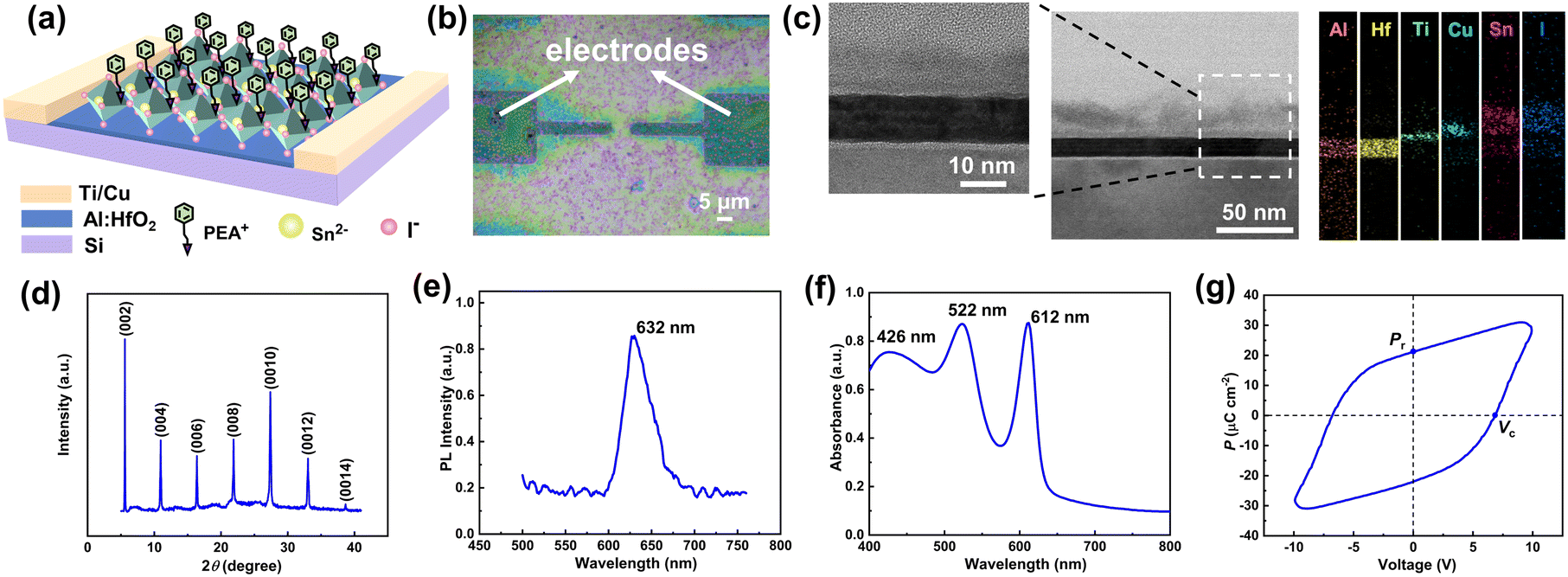 | ||
| Fig. 2 Characterization of the 2D perovskite phototransistor with ferroelectric-gating. (a) The schematic view of the device. (b) The optical microscopy of the as-fabricated phototransistor. (c) The cross-sectional transmission electron microscopy (TEM) image and energy-dispersive spectrometry (EDS) elemental mapping analysis of the developed phototransistor. (d) X-ray diffraction (XRD) pattern of the spin-coated perovskite. (e) Photoluminescence (PL) spectra of the 2D perovskite. (f) Ultraviolet–visible spectra of the deposited perovskite film. (g) Hysteresis loop of the fabricated Al:HfO2 ferroelectric nanofilm; Pr and Vc represent remanent polarization and coercive voltage, respectively. | ||
Polarizable and electrical modulation mechanisms of ferroelectric-gating
The polarizable and electrical modulation is implemented through a localized field induced by remanent polarization. Bipolar pluses with increasing amplitudes up to the coercive voltage of approximately 7 V at 1 kHz are applied at the gate electrode to enhance the coercive window, and then single pulses are triggered to strengthen the stability of polarization. Attributed to the thickness-dependent ferroelectricity, the Al:HfO2 nanofilm contains decent polarization properties at the cost of low breakdown strength with the thickness of 11.1 nm. Hence, the gate voltage is determined to sweep ranging from 20 V to −20 V, which fully enables the gate's switching behaviors. As a result, a nonvolatile and reversable electric field over 108 V m−1 is introduced to regulate transport and contact properties, exhibiting as a clockwise hysteresis loop with an on/off ratio exceeding 106 shown in Fig. 3a. Since the current for backward sweep is higher than that for forward sweep in the transfer curve (Ids–Vg), the ferroelectric polarization is confirmed to prevail the hysteretic mechanism rather than charge trapping. In addition, the voltage dependence of capacitance in the ferroelectric film is measured as shown in the inset of Fig. 3a. The permittivity of Al:HfO2 is calculated to range from 10.5 to 11.9. Based on the slope of the transfer curve and the permittivity of the dielectric layer, the maximum value of the hole field-effect mobility reaches 1.61 cm2 V−1 s−1, according to the following formula:31 | (1) |
 | ||
| Fig. 3 Polarization-related electrical characterization of the proposed phototransistor. (a) Transfer curve (Ids–Vg) of the fabricated device and the inset shows the voltage dependence of capacitance in Al:HfO2 film. (b) The output curves (Ids–Vds) of the ferroelectric-gated phototransistor under Fresh (without polarization), Pup (upward polarization) and Pdown (downward polarization) states. (c) The band diagrams of the perovskite and electrodes in Pup and Pdown states. EC, EF and EV represent the conduction band, Fermi level and valence band of the perovskite, respectively. | ||
To further investigate the effect of Al:HfO2 ferroelectric-gating on phototransistor performances, the output curves (Ids–Vd) under the upward-polarization state (Pup), downward-polarization state (Pdown) and without polarization state (Fresh) are obtained at zero gate voltage as shown in Fig. 3b. When the remanent polarization field is tuned to the Pup state, the electrons are fixed at the interface between the perovskite and Al:HfO2. And the channel transportation induced by dominated carriers of holes would be seriously disturbed by mobile cations. Simultaneously, the contact barrier between the perovskite and metal electrodes enlarges under the upward ferroelectric-gating, which significantly inhibits the conductance of the perovskite, leading to a depressed dark current down to the nanoampere range. Corresponding to the Kelvin probe force microscopy (KPFM) measurements, the surface potential of the perovskite on the ferroelectric film indicates an obvious decrease as the holes are depleted by the negative polarization charges on the top surface of Al:HfO2 shown in Fig. S2,† which is consistent with the suppressed drain current. In contrast, the mobile cations would be attracted by the downward-oriented ferroelectric domains and bounded at the interface, resulting in large and stable flowing currents to occupy the channel. As a result, the accumulation of holes leads to an increase of surface potential as presented in Fig. S2.† At the same time, the contact barrier would decrease attributed to the downward energy band bending of the perovskite, which enables efficient tunneling of holes through the barrier. The working mechanisms and energy band diagrams of the ferroelectric-gated phototransistor are shown in Fig. 3c and 4. Moreover, a SiO2-based phototransistor with the (PEA)2SnI4 channel is intentionally proposed to investigate the contribution of ferroelectric-gating. The transfer curve presents unhysteretic behavior and a restricted on/off ratio over 103, indicating a weak intrinsic switching effect on transport properties as shown in Fig. S3.† The significantly depressed off current for the Al:HfO2-based device reveals that the introduced ferroelectric-gating plays a decisive role in modulating charge dynamics and weakening the Fermi level pinning effect, which enables improved photocurrent extraction. And it is especially promising for application in weak light detection.
 | ||
| Fig. 4 The modulation mechanism of ferroelectric-gating for charge redistribution and ion mitigation in the perovskite phototransistor. | ||
Enhanced optoelectronic performances of the ferroelectric-gated 2D perovskite phototransistor
To better clarify the effect of ferroelectric-gating on improved optoelectronic performances, characterization of the proposed photodetector is performed in the Pup state without an external gate voltage. Under light illumination at 530 nm wavelength, the output curves illustrate a linear and symmetry tendency as shown in Fig. 5a, which indicates the formation of quasi-Ohmic contacts regulated by the ferroelectric-induced nonvolatile electric field. Since charges are attracted by the oriented ferroelectric domains and fixed at the interface, employing as the floating gate, the fabricated device enables ultrasensitive and efficient extraction of the photocurrent from the depressed dark current, which is demonstrated as an outstanding on/off ratio exceeding 107. To further evaluate the photoresponse properties of the ferroelectric-gated phototransistor, typical figures of merits such as responsivity (R) and detectivity (D*) are measured. The responsivity is decided by the photocurrent over illumination light power, reaching the highest value of 4918 A W−1, which is attributed to the high capacity gating. Besides, detectivity is calculated as D* = R(AΔf)1/2/(IS + IT), where A is the photosensitive area, Δf is the bandwidth, IS and IT represent shot noise and thermal noise, respectively.32,33 Owing to the high intrinsic carrier density and long carrier lifetime, the large dark current dominates the channel, which significantly weakens the photodetection capability, resulting in a suppressed detectivity of 8.8 × 10¹² Jones in the Fresh state, as shown in Fig. S4.† Since the 2D perovskite with intense light-harvesting ability serves as an optimized light absorber, along with a ferroelectric-induced electrostatic field employed as a floating gate to efficiently inhibit noise current, the incident light signal could be accurately distinguished, leading to a remarkable detectivity of 2.15 × 10¹⁵ Jones in the Pup state. As for the downward polarization state, the dark current is extremely improved to approximately microampere range and the photocurrent can be hardly extracted. Consequently, the detectivity is limited as 9.8 × 10¹¹ Jones. Moreover, monolayer inorganic sheets sandwiched between long-chain organic layers of the 2D perovskite are used as quantum wells to prolong the carrier lifetime. Meanwhile, the oxygen vacancies introduced in the orthorhombic phase transition process of Al:HfO2 would trap and deplete the generous charges of the perovskite at the interface through defect engineering, contributing to recirculation of photoexcited carriers tunneling from drain to source before recombination. As a result, the fabricated phototransistor exhibits a prominent photogain (G) of 2.1 × 10⁷ and an impressive external quantum efficiency (EQE) of 1.15 × 10⁶%, respectively. Compared with the SiO2-based device, the dark current is higher by orders of magnitude at a high gate voltage of 20 V, which introduces leakage paths and severe disorder. As a result, the ferroelectric-free phototransistor exhibits a poor detectivity of 2.3 × 10¹² Jones as shown in Fig. S3,† which is attributed to the inefficient gate control through an external bias. In addition to the appealing photosensitivity, the time-resolved photoresponse of the ferroelectric-gated device is investigated as shown in Fig. 5c. The rise (τrise) and decay (τdecay) times are estimated as 226.1 and 322.4 ms, respectively, due to the modulation of the long carrier lifetime that significantly boosts the photoelectric conversion efficiency via inhibited charge recombination at the cost of response speed. | ||
| Fig. 5 Optoelectronic properties of the 2D perovskite phototransistor with ferroelectric-gating under the Pup state without a constant gate bias. (a) The output curves of the fabricated device under varied illumination powers. (b) The incident light power dependence of responsivity (R) and detectivity (D*) at Vds = 1 V. (c) The rise and decay times of the device. (d) The comparison of photoresponse performances corresponding to responsivity and detectivity between the proposed device and previously reported perovskite-based phototransistors. QDs, quantum dots; PEDOT:PSS, poly-(3,4-ethylenedioxythiophene):poly(styrenesulfonate); DTTQ, dithienothiophenoquinoid. | ||
A comparison between the proposed ferroelectric-gated phototransistor and previously reported perovskite-based devices is made to benchmark the photoresponse performances as shown in Fig. 5d,4,5,7,8,16–18,20,34–39 which exhibits several characteristics: (i) An outstanding detectivity of up to 2.15 × 10¹⁵ Jones along with an impressive responsivity of 4918 A W−1 indicate superior overall optoelectronic performances compared with previous works, which demonstrates an accurate and highly efficient photocurrent extraction from the considerably depressed noise current, especially in weak light detection. (ii) High-capacity ferroelectric-gating induced by nonvolatile remanent polarization provides a reversible and stable localized electrostatic field to modulate channel transport properties, charge redistributions and band alignments without requiring an external gate voltage, which contributes a significant reduction of power consumption compared with that of the reported devices working under a high gate bias up to −70 V.8 (iii) An ultrathin dielectric layer at the sub-15 nm scale remarkably facilitates improved gating efficiency, high-levels of device integration and scalability as well as miniaturization.
Conclusions
In conclusion, we developed an ultrasensitive gate-bias-free phototransistor based on the highly photoactive 2D perovskite (PEA)2SnI4 and the functional ferroelectric nanofilm of Al:HfO2. The polarized ferroelectric domains induced a nonvolatile and reversible localized field of up to 108 V m−1 through the electrostatic effect, which served as a floating gate to depress ion migration, define charge redistributions and regulate the contact barrier. Besides, the layered structure of the proposed device introduced defect engineering and inhibited carrier scattering, which was attributed to additional quantum wells and oxygen vacancies, considerably facilitating efficient charge transport and high gating efficiency. As a result, a prominent responsivity of 4918 A W−1 and a detectivity of 2.15 × 10¹⁵ Jones have been achieved at zero gate voltage, which are appealing values compared with those of previously reported devices working under high gate bias. The device's high capacity for polarizable nonvolatile ferroelectric-gating, sensitive photodetection capabilities and high scalability contribute to advancements in applications such as large-scale sensor arrays, flexible optoelectronics, solar cells, light-wave communications and imaging technology.Experimental section
Material preparation
An Al:HfO2 ferroelectric nanofilm with 8 mol% Al dopant concentration was prepared by atomic layer deposition (ALD) at 280 °C/20 Pa, where liquid tetrakis (diethylamide) hafnium (TDMAH), trimethyl aluminum (TMA) and O2 plasma served as precursors for Hf, Al and oxygen, respectively. And then the films were processed through rapid thermal annealing (RTA) at 750 °C for 30 s to crystallize.Device fabrication
The patterned source/drain electrodes of Ti/Cu were defined by standard ultraviolet lithography and thermally deposited through the lift-off process. For the blade-coating process, 2-phenylethylammonium iodide (PEAI) and SnI2 were dissolved in dimethylacetamide (DMF) with a stoichiometric ratio of 2![[thin space (1/6-em)]](https://www.rsc.org/images/entities/char_2009.gif) :1 to prepare precursor solutions, whose concentration was set to 0.2 mol L−1. For film fabrication, 100 μL of the precursors was added dropwise onto Al:HfO2 substrates with deposited electrodes, which have been modified by ultraviolet ozone surface treatment, and then spin-coated at 4000 rpm for 30 s. Afterwards, the coated films were annealed at 100 °C for 10 min to rapidly crystallize. To improve the stability in ambient air, the fabricated devices were spin-coated with polymethyl methacrylate (PMMA) at 2000 rpm for 60 s. After baking at 100 °C for 10 min, the encapsulated phototransistor based on the 2D perovskite and ferroelectric-gating were obtained. The microscopy image of the as-fabricated device under illumination is shown in Fig. S1.†
:1 to prepare precursor solutions, whose concentration was set to 0.2 mol L−1. For film fabrication, 100 μL of the precursors was added dropwise onto Al:HfO2 substrates with deposited electrodes, which have been modified by ultraviolet ozone surface treatment, and then spin-coated at 4000 rpm for 30 s. Afterwards, the coated films were annealed at 100 °C for 10 min to rapidly crystallize. To improve the stability in ambient air, the fabricated devices were spin-coated with polymethyl methacrylate (PMMA) at 2000 rpm for 60 s. After baking at 100 °C for 10 min, the encapsulated phototransistor based on the 2D perovskite and ferroelectric-gating were obtained. The microscopy image of the as-fabricated device under illumination is shown in Fig. S1.†
Characterization and measurements
The characterization of the morphology and crystallinity was performed by optical microscopy (OM, Olympus BX51-P), X-ray diffraction (XRD, Bruker, New D8 Advance), ultraviolet–visible spectrophotometry (Agilent, Cary 5000 UV-Vis-NIR), and photoluminescence spectroscopy (PL, Renishaw inVia confocal Raman system). The electrical and optical measurements were carried out at room temperature in ambient air using a semiconductor parameter analyzer (Keithley, Semiconductor Characterization System 4200A-SCS) equipped with a 530 nm laser diode.Author contributions
G. M. and J. S. conceived the idea and designed the research. J. S. carried out most of the experimental work. X. L. helped with the deposition and dielectric measurements of Al:HfO2. H. C. and J. X. assisted with the preparation of the perovskite. G. M., J. S., Z. S., J. W. and Y. C. wrote the manuscript with input from all the other authors. All authors were involved in extensive discussions and data analyses.Data availability
Data for this article “A ferroelectrically modulated ultrasensitive two-dimensional perovskite phototransistor with zero-gate-bias”, including the ferroelectric properties of remanent polarization in Al:HfO2 nanofilm, such as the bipolar excitation method, field strength and switching persistence are available from ACS Publications at: https://pubs.acs.org/doi/full/10.1021/acsami.3c15533.Conflicts of interest
The authors declare no competing interests.Acknowledgements
The authors thank Pengcheng Zhang of Xi'an Jiaotong University for his assistance with FIB analyses. Meanwhile, the authors thank Chao Li at the Instrument Analysis Center of Xi'an Jiaotong University for technical assistance with TEM. Moreover, the authors thank associate professor Jun Zhou and Ming Wu of Xi'an Jiaotong University for their assistance with KPFM and the polarization method, respectively.References
- C. Li, Y. Ma, Y. Xiao, L. Shen and L. Ding, InfoMat, 2020, 2, 1247–1256 CrossRef CAS.
- Y. Zhang, Y. Ma, Y. Wang, X. Zhang, C. Zuo, L. Shen and L. Ding, Adv. Mater., 2021, 33, 2006691 CrossRef CAS PubMed.
- F. Cao and L. Li, Adv. Funct. Mater., 2021, 31, 2008275 CrossRef CAS.
- M. J. Loes, A. Lipatov, N. S. Vorobeva, H. Lu, J. Abourahma, D. S. Muratov, A. Gruverman and A. Sinitskii, ACS Appl. Electron. Mater., 2023, 5, 705–713 CrossRef CAS.
- J. Wu, Y. Miao, X. Qi, L. Yang, X. Wang, F. Zheng, F. Zhao, S. Shafique and Z. Hu, ACS Photonics, 2023, 10, 4437–4446 CrossRef CAS.
- C.-K. Liu, H.-L. Loi, J. Cao, G. Tang, F. Liu, Q. Huang, X. Liang and F. Yan, Small Struct., 2021, 2, 2000084 CrossRef CAS.
- K. Yun, T. Lee, S. Kim, J. Kim and T. Seong, Adv. Opt. Mater., 2023, 11, 2201974 CrossRef CAS.
- H. Loi, J. Cao, C. Liu, Y. Xu, M. G. Li and F. Yan, Small, 2023, 19, 2205976 CrossRef CAS PubMed.
- F. Wang, X. Zou, M. Xu, H. Wang, H. Wang, H. Guo, J. Guo, P. Wang, M. Peng, Z. Wang, Y. Wang, J. Miao, F. Chen, J. Wang, X. Chen, A. Pan, C. Shan, L. Liao and W. Hu, Adv. Sci., 2021, 8, 2100569 CrossRef CAS PubMed.
- Y. Wu, W. Chen, G. Chen, L. Liu, Z. He and R. Liu, Nanomaterials, 2018, 8, 356 CrossRef PubMed.
- G. Abiram, M. Thanihaichelvan, P. Ravirajan and D. Velauthapillai, Nanomaterials, 2022, 12, 2396 CrossRef CAS PubMed.
- S. Li, X. Liu, H. Yang, H. Zhu and X. Fang, Nat. Electron., 2024, 7, 216–224 CrossRef CAS.
- F. Zhang, Q. Zhang, X. Liu, L. Qin, Y. Hu, Z. Lou, Y. Hou and F. Teng, J. Mater. Chem. A, 2021, 9, 22842–22853 RSC.
- H. Zhu, A. Liu, T. Zou, H. Jung, S. Heo and Y.-Y. Noh, Mater. Today Energy, 2021, 21, 100722 CrossRef CAS.
- X. Huang, Q. Li, W. Shi, K. Liu, Y. Zhang, Y. Liu, X. Wei, Z. Zhao, Y. Guo and Y. Liu, Small, 2021, 17, 2102820 CrossRef CAS PubMed.
- C.-K. Liu, Q. Tai, N. Wang, G. Tang, Z. Hu and F. Yan, ACS Appl. Mater. Interfaces, 2020, 12, 18769–18776 CrossRef CAS PubMed.
- T. Chen, C. Wang, G. Yang, Q. Lou, Q. Lin, S. Zhang and H. Zhou, Adv. Mater. Technol., 2023, 8, 2200679 CrossRef CAS.
- M. He, Z. Xu, C. Zhao, Y. Gao, K. Ke, N. Liu, X. Yao, F. Kang, Y. Shen, L. Lin and G. Wei, Adv. Funct. Mater., 2023, 33, 2300282 CrossRef CAS.
- Y. Ju, X. Wu, S. Huang, G. Dai, T. Song and H. Zhong, Adv. Funct. Mater., 2022, 32, 2108296 CrossRef CAS.
- H. Jing, R. Peng, R.-M. Ma, J. He, Y. Zhou, Z. Yang, C.-Y. Li, Y. Liu, X. Guo, Y. Zhu, D. Wang, J. Su, C. Sun, W. Bao and M. Wang, Nano Lett., 2020, 20, 7144–7151 CrossRef CAS PubMed.
- H. Zhu, A. Liu, H. L. Luque, H. Sun, D. Ji and Y.-Y. Noh, ACS Nano, 2019, 13, 3971–3981 CrossRef CAS PubMed.
- T. Tong, Y. Gan, W. Li, W. Zhang, H. Song, H. Zhang, K. Liao, J. Deng, S. Li, Z. Xing, Y. Yu, Y. Tu, W. Wang, J. Chen, J. Zhou, X. Song, L. Zhang, X. Wang, S. Qin, Y. Shi, W. Huang and L. Wang, ACS Nano, 2023, 17, 530–538 CrossRef CAS PubMed.
- X. D. Wang, P. Wang, J. Wang, W. D. Hu, X. H. Zhou, N. Guo, H. Huang, S. Sun, H. Shen, T. Lin, M. H. Tang, L. Liao, A. Q. Jiang, J. L. Sun, X. J. Meng, X. S. Chen, W. Lu and J. H. Chu, Adv. Mater., 2015, 27, 6575–6581 CrossRef CAS PubMed.
- Q. Chen, D. Lai, L. He, Y. Yan, E. Li, Y. Liu, H. Zeng, H. Chen and T. Guo, ACS Appl. Mater. Interfaces, 2021, 13, 1035–1042 CrossRef CAS PubMed.
- B. Jeong, L. Veith, T. J. A. M. Smolders, M. J. Wolf and K. Asadi, Adv. Mater., 2021, 33, 2100486 CrossRef CAS PubMed.
- B. Jeong, P. Gkoupidenis and K. Asadi, Adv. Mater., 2021, 33, 2104034 CrossRef CAS PubMed.
- F. Cao, W. Tian, L. Meng, M. Wang and L. Li, Adv. Funct. Mater., 2019, 29, 1808415 CrossRef.
- F. Li, C. Ma, H. Wang, W. Hu, W. Yu, A. D. Sheikh and T. Wu, Nat. Commun., 2015, 6, 8238 CrossRef PubMed.
- J.-Y. Go, H. Zhu, Y. Reo, H. Kim, A. Liu and Y.-Y. Noh, ACS Appl. Mater. Interfaces, 2022, 14, 9363–9367 CrossRef CAS PubMed.
- R. Li, C. Yi, R. Ge, W. Zou, L. Cheng, N. Wang, J. Wang and W. Huang, Appl. Phys. Lett., 2016, 109, 151101 CrossRef.
- L. Q. Tu, R. Cao, X. D. Wang, Y. Chen, S. Q. Wu, F. Wang, Z. Wang, H. Shen, T. Lin, P. Zhou, X. J. Meng, W. D. Hu, Q. Liu, J. L. Wang, M. Liu and J. H. Chu, Nat. Commun., 2020, 11, 101 CrossRef CAS PubMed.
- Y. Chen, Y. Wang, Z. Wang, Y. Gu, Y. Ye, X. Chai, J. Ye, Y. Chen, R. Xie, Y. Zhou, Z. Hu, Q. Li, L. Zhang, F. Wang, P. Wang, J. Miao, J. Wang, X. Chen, W. Lu, P. Zhou and W. Hu, Nat. Electron., 2021, 4, 357–363 CrossRef CAS.
- C. R. Paul Inbaraj, R. J. Mathew, R. Sankar, H. Y. Lin, N.-X. Li, Y.-T. Chen and Y.-F. Chen, ACS Appl. Mater. Interfaces, 2023, 15, 19121–19128 CrossRef CAS PubMed.
- Y. Zou, T. Zou, C. Zhao, B. Wang, J. Xing, Z. Yu, J. Cheng, W. Xin, J. Yang, W. Yu, H. Dong and C. Guo, Small, 2020, 16, 2000733 CrossRef CAS PubMed.
- C. Fang, H. Wang, Z. Shen, H. Shen, S. Wang, J. Ma, J. Wang, H. Luo and D. Li, ACS Appl. Mater. Interfaces, 2019, 11, 8419–8427 CrossRef CAS PubMed.
- A. A. Hussain, A. K. Rana and M. Ranjan, Nanoscale, 2019, 11, 1217–1227 RSC.
- C. Liu, Q. Tai, N. Wang, G. Tang, H. Loi and F. Yan, Adv. Sci., 2019, 6, 1900751 CrossRef PubMed.
- S.-J. Jeong, S. Cho, B. Moon, J. A. Teku, M.-H. Jeong, S. Lee, Y. Kim and J.-S. Lee, ACS Appl. Mater. Interfaces, 2023, 15, 5432–5438 CrossRef CAS PubMed.
- S.-H. Hong, S. N. Afraj, P.-Y. Huang, Y.-Z. Yeh, S.-H. Tung, M.-C. Chen and C.-L. Liu, Nanoscale, 2021, 13, 20498–20507 RSC.
Footnote |
| † Electronic supplementary information (ESI) available. See DOI: https://doi.org/10.1039/d4nr04910a |
| This journal is © The Royal Society of Chemistry 2025 |