
 Open Access Article
 This Open Access Article is licensed under a Creative Commons Attribution-Non Commercial 3.0 Unported Licence
Small-rotation-angle moiré structures of 2H TaSe2 monolayers on Au(111)†
Lina
Liu
 *abc,
Dmitry Y.
Zemlyanov
c and
Yong P.
Chen
*abcd
*abc,
Dmitry Y.
Zemlyanov
c and
Yong P.
Chen
*abcd
aDepartment of Physics and Astronomy, Purdue University, West Lafayette, Indiana 47907, USA. E-mail: yongchen@purdue.edu; lina.liu@epfl.ch
bDepartment of Physics and Astronomy and Villum Center for Hybrid Quantum Materials and Devices, Aarhus University, 8000 Aarhus C, Denmark
cBirck Nanotechnology Center, Purdue University, West Lafayette, Indiana 47907, USA
dPurdue Quantum Science and Engineering Institute and School of Electrical and Computer Engineering, Purdue University, West Lafayette, Indiana 47907, USA
First published on 19th February 2025
Abstract
Direct synthesis of two-dimensional (2D) materials with moiré patterns can provide 2D moiré structures with a clean interface and be useful for future electronics applications. However, the synthesis of moiré structures with small rotation angles is challenging since such structures possess the tendency to untwist during high temperature synthesis. Here, we study the moiré structures formed by epitaxially grown 2H TaSe2 monolayers on Au(111). By resolving atomic configurations using scanning tunneling microscopy (STM), we reveal the as-grown TaSe2 monolayers demonstrate small rotation angles between 0° to 3° with respect to the underlying Au lattices. We demonstrate that the deposition sequence of Se and Ta during growth can make an important difference: first depositing Se on Au predominantly gives small rotation angles, while first depositing Ta on Au predominantly results in perfectly aligned lattices. Further, we unveil that defects, including hole and line defects, are closely related to the changing orientations of moiré superlattices. Our work provides important insights for the synthesis of small-twist-angle moiré structures and will facilitate future studies of TaSe2 and moiré physics and devices in general.
Moiré patterns are superlattice patterns, formed for example when a two-dimensional (2D) layer is stacked on another lattice with lattice mismatch or a twist angle. The large periodicity (compared to that of the original lattice) moiré potential not only affects atomic structures, but also changes electronic bands. Recently, a variety of fascinating quantum states and phenomena has been reported in 2D van der Waals (vdW) moiré structures, including for example unconventional superconductivity and Mott insulating states in magic-angle (special twist angles typically smaller than 2° in twisted multilayer graphene1) graphene superlattices,2,3 quantum trapped excitons4,5 and fractional topological states in twisted transition metal dichalcogenides (TMDCs) bilayers6–9 and moiré magnetism in twisted 2D magnets.10–12
Moiré patterns in 2D vdW structures can be prepared by artificially stacking the mechanically exfoliated 2D layer on another with a twist angle, which can be controlled by a tunable experimental transfer stage. With this approach, one can in principle produce any twist angles and thus fabricate different designed moiré superstructures. However, the interlayer contamination, as well as lack of mass production and twist angle precision of this method hinder further applications of 2D vdW moiré structures in future twistronics. Direct synthesis of moiré structures can produce a clean interface and hold the potential of scalable synthesis, thus overcoming the limitations of mechanical exfoliation. By lattice mismatch engineering, hetero-site nucleation or using pre-rotated substrates, twisted 2D TMDCs and bilayer graphene have been synthesized.13–17 However, controllable synthesis of moiré superlattices with small twist angles is difficult. The ability to achieve small twist angles is of special interest, for example, in magic-angle graphene systems and other twisted structures when a relatively large moiré periodicity is desired for electronic state engineering or device applications.2,10
Previous studies of 2D materials grown on single crystals have shown occasional growth of moiré superlattices with small rotation angles.18–20 Factors such as interaction strength, strain and interfacial adlayers have been widely discussed and demonstrated to play crucial roles in the final patterns and rotation angles.21–23 These results highlight the potential of growing 2D materials on single-crystalline lattices, for the achievement of controllable growth of small-rotation-angle moiré structures.
Here we explore the moiré structures formed by epitaxially grown 2H TaSe2 monolayers on Au(111). TaSe2 in its 2H phase is a well-known metallic layered/2D material with interesting physical properties ranging from charge density wave (CDW) to superconductivity.24–28 We resolve the topographic and atomic structures of the moiré patterns by scanning tunneling microscopy (STM) and confirm the 2H phase of as-grown TaSe2 by an ultrahigh vacuum (UHV) multiprobe surface analysis system, including STM, X-ray photoelectron spectroscopy (XPS) and high-resolution electron energy loss spectroscopy (HREELS). We reveal that the as-grown 2H TaSe2 flakes demonstrate a variety of small rotation angles spanning from 0° to 3°, which may result from thermal fluctuation induced by Se at the interface of TaSe2 and Au. Further analysis shows that defects are associated with changing moiré orientations. Changing the deposition sequence to first depositing Ta (instead of Se) on Au gives predominantly alighted lattices (instead of small twisting angles). Our work opens up an avenue for the synthesis of moiré patterns with small twist angles and may facilitate the future exploration of moiré physics and devices.
TaSe2 monolayer flakes were synthesized on Au(111) in an UHV environment. Se and Ta were deposited sequentially on a freshly cleaned Au surface by thermal and sputtering deposition, respectively. After annealing at 400 °C in protective Se flux, TaSe2 triangular islands were epitaxially grown on the Au surface (Fig. 1(a), see growth details in the ESI Fig. S1 and S2†). The samples were then characterized by STM at room temperature, at which one does not expect to observe CDW phases24–26 (typically occurring below 120 K) of 2H TaSe2. In the magnified STM topographic image, a big TaSe2 island (constructed by a few triangular TaSe2 flakes joined together) displays a hexagonal periodic pattern with a relatively large periodicity of 16.0 ± 0.3 Å (Fig. S3a,† where error is the standard deviation from different measurements at different positions). This large-periodicity hexagonal pattern, as discussed below, is the moiré pattern formed between TaSe2 monolayer and underlying Au (111). The height of the flake is ∼2.2 Å (Fig. S3b†), comparable with the height of monolayer TMDCs grown on Au(111).19 This height is smaller than the interlayer distance in bulk TaSe2 (∼6.1 Å),29 possibly due to the strong interaction between TaSe2 and Au(111) or a reduced tip–sample tunneling conductance.19 Further, atomic resolution STM was carried out to understand the moiré pattern. In Fig. 1(b), except for the large pattern, hexagonal atom arrays with the periodicity of 3.44 ± 0.14 Å were observed, consistent with the lattice constants of TaSe2.29 Meanwhile, it is clearly seen that the lattices of moiré and TaSe2 are not aligned perfectly, but with a rotation angle of φ = 6.0° ± 0.9° between them, which was also distinguished in the 2D fast Fourier transform (FFT) image (Fig. 1(c)). 2D FFT demonstrates two sets of hexagonal patterns, representing the reciprocal lattices of moiré and TaSe2. The angle between the two lattice vectors kmoiré and kTaSe2 is 5.8° ± 0.6°, close to the rotation angle observed in the real space STM image (Fig. 1(c), φ = 6.0 ± 0.9°). The epitaxial relation among the TaSe2 overlayer lattice, underlying Au(111) lattice and moiré superlattice can be demonstrated by the following equation of reciprocal lattice vectors: kmoiré = kTaSe2 − kAu(111) (inset of Fig. 1(c)). Since the magnitude of reciprocal space vector for a hexagonal lattice k is  (a is the lattice constant in real space), one can calculate the rotation angle θ = 1.0° ± 0.1° between the TaSe2 and underlying Au(111) by using measured amoiré = 16.0 ± 0.3 Å, aTaSe2 = 3.44 ± 0.14 Å and φ = 5.8° ± 0.6°. Note the lattice constant of Au(111) was not involved in the calculation for rotation angle θ. With the above method, we obtained a calculated lattice constant for Au of 2.84 ± 0.04 Å, in reasonable agreement with the known lattice constant of Au(111) of 2.88 Å.30
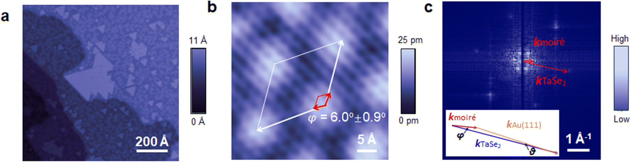 | ||
| Fig. 1 Epitaxially grown TaSe2 monolayer flakes on Au(111). (a and b) STM images of topographic and atomic structures of the as-grown TaSe2 monolayer flakes. The white and red rhombuses indicate the moiré and TaSe2 unit cells, respectively. The white and red arrows are the lattice vectors of moiré and TaSe2 lattices, respectively. The rotation angle between moiré and TaSe2 lattice vectors is φ. (c) A 2D FFT image of Fig. S4,† which is a bigger-area STM image taken on the same TaSe2 flake as that in (b). The red arrows represent reciprocal lattice vectors of moiré and TaSe2 lattices. Inset: the relation between reciprocal lattice vectors of moiré, TaSe2 and Au(111) lattices. φ and θ represent the rotation angle between lattices of moiré and TaSe2, and between TaSe2 and Au(111), respectively. STM measurement conditions: Vb = −0.5 V, It = 1.0 nA. | ||
Since TaSe2 can present both 2H and 1 T phases and they exhibit different atomic configurations,29 XPS and HREELS were further conducted to confirm the phase of the as-grown TaSe2. Core-levels of Ta measured by XPS show one set of peaks at the binding energies of 23.5 eV and 25.4 eV (Fig. 2(a)), corresponding to Ta 4f7/2 and 4f5/2 orbitals in 2H TaSe2, respectively31 (different from those of 1T TaSe2 at 22.6 eV and 24.4 eV32). Meanwhile, XPS spectra of Se 3d exhibit two sets of peaks. The peaks at lower binding energies of 53.7 eV and 54.6 eV (Fig. 2(b)) are close to those of 2H TaSe2 at 53.6 eV and 54.5 eV31 (different from those of 1T TaSe2 at 53.3 eV and 54.1 eV32). In addition, we also observed a minor set of Se components at the binding energies of 55.4 eV and 56.3 eV, close to those of elemental Se (55.6 eV and 56.5 eV).33 Interestingly, these components were absent when we switched the deposition sequence of Se and Ta during growth (i.e., depositing Ta before Se, detailed discussions of growth with different deposition sequences could be found in the following text). The minor set of Se peaks could be possibly attributed to elemental Se at the interface between TaSe2 and Au(111). Moreover, two electron energy loss signals were detected at 26 meV and 31 meV (Fig. 2(c)) by HREELS, in fair agreement with the characteristic E2g and A1g phonon modes34 (215 cm−1 and 233 cm−1, equal to ∼27 meV and ∼29 meV, respectively) of monolayer 2H TaSe2 previously measured by Raman spectroscopy and significantly different from those of 1T TaSe2 at ∼185 cm−1 (∼23 meV) and ∼105 cm−1 (∼13 meV),32 confirming the 2H phase of the as-grown TaSe2.
 | ||
| Fig. 2 XPS and HREELS spectra of the as-grown TaSe2 monolayers. (a and b) XPS core-level spectra of Ta and Se, respectively. Dark blue lines and black circles denote the fitted and raw data, respectively. Black lines are backgrounds. Purple peaks in (a) represent the fitted components for Ta. Yellow and green peaks in (b) represent the fitted components for Se. The light blue peak in (b) represents the Au 5p3/2 peak. Fitting details are shown in the ESI Table S1.† (c) HREELS spectra of the as-grown TaSe2 monolayers. Inset: a zoomed-in spectrum of (c) after background subtraction. | ||
To understand the moiré structures of 2H TaSe2 monolayers on Au(111), we analyzed 51 TaSe2 flakes based on three experimental batches and obtained the statistical distribution of the rotation angles between the as-grown TaSe2 and Au(111). It should be noted that, to ensure high quality STM images, typical sizes of the analyzed flakes are above ∼8 nm. Fig. 3(a)–(c) display three representative moiré patterns. Although they all present hexagonal moiré patterns, it can be seen that the orientations between the lattice of moiré and TaSe2 are different. Detailed analysis confirms that the rotation angles (θ) between TaSe2 and Au(111) in these three cases are 0.46° ± 0.04°, 1.3° ± 0.06° and 2.3° ± 0.09° (Fig. 3(a)–(c), respectively). All the analyzed angles are found to range from 0° to 3° and their distribution is shown in Fig. 3(d). TaSe2 flakes with rotation angles between 1.0° and 1.5° occupy the biggest population (∼32%), and ∼82% of the as-grown flakes exhibit rotations between 0.5° and 2.0°.
 | ||
| Fig. 3 Different moiré orientations of 2H TaSe2 monolayers on Au(111). (a–c) Atomic scale STM images of the moiré structures on three different TaSe2 flakes. Vb = −1.0 V, It = 1.0 nA. The angle between moiré and TaSe2 lattices is represented by φ. The rotation angle between TaSe2 and Au(111) lattices is represented by θ. The white and red rhombuses indicate the moiré and TaSe2 unit cells, respectively. Note the crystal orientations of Au(111) are different in (a–c) (indicated by the yellow arrows). It is because (a–c) are results from different experimental batches and the Au(111) crystal was remounted a few times during the experiment. (d) Distribution of the rotation angle θ based on the analyzed 51 TaSe2 flakes. | ||
Further, we investigated the origin of the small rotation angles. We observed that the overall lattice rotations of the as-grown TaSe2 exhibit strong dependence on the deposition sequence of Se and Ta in the growth. When Se was first deposited on Au, TaSe2 is likely to present various small rotation angles (schematically depicted in Fig. 4(a)) as discussed above. In contrast, when Ta was first deposited on Au, TaSe2 mostly demonstrates perfectly aligned lattices (schematically depicted in Fig. 4(b)). Topographic and atomic resolution moiré structures of TaSe2 grown by first depositing Ta on Au are shown in Fig. 4(c) and (d), respectively (more details in Fig. S5†). It can be seen that the orientations of moiré superlattice and TaSe2 lattice are perfectly aligned with each other, suggesting a 0° rotation relation between TaSe2 and underlying Au lattice. The periodicity of the moiré superlattice is 16.2 ± 0.1 Å. Further analysis (Fig. 4(e)) of 47 TaSe2 flakes shows that θ = 0° dominates the rotation angles, accounting for ∼88% of the analyzed flakes, dramatically different from the case when Se was deposited first on Au. We attribute this intriguing difference to the interfacial fluctuation induced by Se at the interface of TaSe2 and Au(111). Since it is known that interfacial intercalation can trigger twisting in 2D layers,35 when Se is first deposited on Au, it is possible that interfacial Se forms on Au(111) upon annealing,23,36 generating thermal fluctuations and resulting in the growth of TaSe2 with small rotation angles. In contrast, when Ta is first deposited on Au, no interfacial Se exists between TaSe2 and Au (Fig. 4(f), compared with Fig. 2(b), only Se XPS peaks corresponding to 2H TaSe2, at the binding energies of 53.7 eV and 54.6 eV, were observed). Therefore, TaSe2 prefers the perfectly aligned lattices on Au(111). To confirm the existence/lack of interfacial Se, further characterizations by other surface-sensitive and high-resolution techniques such as synchrotron XPS37,38 and X-ray standing wave (XSW)37,38 are worth considering in future studies.
 | ||
| Fig. 4 Moiré structures of 2H TaSe2 on Au with different deposition sequences. (a and b) Schematic illustrations of moiré structures of 2H TaSe2 on Au when changing the deposition sequence of Se and Ta, respectively. (c and d) Topographic and atomic structures images of the perfectly aligned TaSe2 lattices on Au, respectively. Vb = −1.0 V, It = 1.0 nA. The white and red rhombuses in (c) and (d) indicate the moiré and TaSe2 unit cells, respectively. The white and red arrows in (d) are the lattice vectors of moiré and TaSe2 lattices, respectively. (e) Distribution of the rotation angle θ based on the analyzed 47 TaSe2 flakes grown by depositing Ta first on Au in the growth. (f) Se 3d XPS spectra on a sample grown by depositing Ta first on Au(111). Black circles and dark blue curves represent raw and fitted curves, respectively. Yellow components are Se in TaSe2. The light blue component is the Au 5p3/2 peak. | ||
We also observed that changes in the orientations of moiré superlattices appeared along with defects formed during the growth. Fig. 5(a) shows the continuity of the moiré superlattice is disrupted by a hole defect in the TaSe2 flake. With the hole defect in the center, an area within ∼8 nm from the defect is obviously distorted. Moiré orientations could also be affected by line defects (e.g. edges and grain boundaries). The orientation of the moiré superlattice in Fig. 5(b) demonstrates a sudden rotation of 20° inside a single triangular flake, indicating two lattice orientations in this flake. This is unusual for a single synthesized triangular TMDC flake because it typically exhibits single crystallinity within the entire flake.39,40 The different lattice orientations could possibly be attributed to strain induced during growth from the edges.41 This phenomenon was also observed when two TaSe2 flakes are connected by a grain boundary. In Fig. 5(c), two moiré superlattices exhibit an angle of 9° between them, separated by a grain boundary that makes a change in the orientations of the two moiré superlattices.
 | ||
| Fig. 5 Moiré orientations near defects. (a) Moiré structures affected by a hole defect. The black dashed circle approximately outlines the area of moiré lattices that are disturbed. (b and c) Moiré orientations affected by line defects. The two black arrows in (b) point to the edges of the flake (and another flake at lower left). Dashed white lines in (b) and (c) are guides for eyes for the orientations of moiré superlattices. Black dashed lines in (b) and (c) approximately indicate the boundaries where moiré patterns change orientations. Vb = −0.5 V, It = 1.0 nA. | ||
It has been well-known that defects in 2D materials are actively involved in triggering local atomic reconstruction,42 creating novel atomic structures,43 inducing atomic movement and phase transitions.42,44 Here, defects may play a role in inducing local atomic migration and strain field,45,46 thus contributing to lattice rotations. To further clarify the role of defects in moiré formation, atomic-scale dynamic imaging approaches, such as transmission electron microscopy (TEM), could be conducted in future. With electron beam irradiation during imaging, real-time defect formation and its role in disturbing moiré patterns could be further studied.
Conclusions
In summary, we demonstrated the epitaxial growth of TaSe2 monolayers on Au(111) and the moiré structures formed by the two lattices. The 2H phase of the as-grown TaSe2 was confirmed by the observation of characteristic binding energies in XPS and phonon modes in HREELS spectra. Further, by resolving atomic structures characterized using STM, we observed different rotation angles between the as-grown TaSe2 lattices and the moiré superlattices. Statistical analysis showed that the TaSe2 lattices exhibited small rotation angles with respect to the underlying Au(111) lattices, ranging from 0° to 3°, with most rotation angles between 1.0° and 1.5°. More importantly, we illustrated that the small-rotation-angle moiré structures were likely to grow when Se was first deposited on Au. Depositing Ta first leads to the dominant growth of perfectly aligned TaSe2 lattices. This difference may result from interfacial Se which disturbs lattice alignment and weakens sample-substrate interaction during growth. An interesting comparison may be made with, for example, the role of a 2D material in remote epitaxy,47,48 where interfacial interactions are also weakened. Our approach and findings (such as the deposition order of different elements may lead to different alignments) may offer new insights to enhance the control of other methods of 2D materials growth (such as remote epitaxy), thereby facilitating the fabrication of advanced semiconductors and oxide films for future electronics. In addition, we demonstrated that defects, including hole and line defects, can be associated with changing orientations of moiré superlattices. Our work sheds new light on the understanding of synthesized moiré structures. Future studies, such as using a 2D single crystal substrate or proper interfacial engineering, can be conducted for the general synthesis of 2D moiré vdW structures particularly with small rotation angles, thus promoting both their fundamental studies and twistronic applications.Author contributions
L.L. conceived the idea and designed the experiments. L.L. and D.Y.Z. performed the experiments and data analysis, with advice from Y.P.C. All authors co-wrote the paper and gave approval of the final version.Data availability
Data related to this paper are available from the corresponding author upon reasonable request.Conflicts of interest
There are no conflicts to declare.Acknowledgements
This experimental work was supported by the U.S. Department of Energy (Office of Basic Energy Sciences) under Award No. DE-SC0019215 and Multidisciplinary University Research Initiatives (MURI) Program under Award No. FA9550-20-1-0322. We also acknowledge the Villum Investigator program (Grant No. 25931) for supporting the data analysis.References
- E. Khalaf, A. J. Kruchkov, G. Tarnopolsky and A. Vishwanath, Phys. Rev. B, 2019, 100, 085109 CrossRef CAS.
- Y. Cao, V. Fatemi, S. Fang, K. Watanabe, T. Taniguchi, E. Kaxiras and P. Jarillo-Herrero, Nature, 2018, 556, 43–50 CrossRef CAS PubMed.
- Y. Cao, V. Fatemi, A. Demir, S. Fang, S. L. Tomarken, J. Y. Luo, J. D. Sanchez-Yamagishi, K. Watanabe, T. Taniguchi, E. Kaxiras, R. C. Ashoori and P. Jarillo-Herrero, Nature, 2018, 556, 80–84 CrossRef CAS PubMed.
- K. Tran, G. Moody, F. Wu, X. Lu, J. Choi, K. Kim, A. Rai, D. A. Sanchez, J. Quan, A. Singh, J. Embley, A. Zepeda, M. Campbell, T. Autry, T. Taniguchi, K. Watanabe, N. Lu, S. K. Banerjee, K. L. Silverman, S. Kim, E. Tutuc, L. Yang, A. H. MacDonald and X. Li, Nature, 2019, 567, 71–75 CrossRef CAS PubMed.
- K. L. Seyler, P. Rivera, H. Yu, N. P. Wilson, E. L. Ray, D. G. Mandrus, J. Yan, W. Yao and X. Xu, Nature, 2019, 567, 66–70 CrossRef CAS PubMed.
- J. Cai, E. Anderson, C. Wang, X. Zhang, X. Liu, W. Holtzmann, Y. Zhang, F. Fan, T. Taniguchi, K. Watanabe, Y. Ran, T. Cao, L. Fu, D. Xiao, W. Yao and X. Xu, Nature, 2023, 622, 63–68 CrossRef CAS PubMed.
- H. Park, J. Cai, E. Anderson, Y. Zhang, J. Zhu, X. Liu, C. Wang, W. Holtzmann, C. Hu, Z. Liu, T. Taniguchi, K. Watanabe, J. H. Chu, T. Cao, L. Fu, W. Yao, C. Z. Chang, D. Cobden, D. Xiao and X. Xu, Nature, 2023, 622, 74–79 CrossRef CAS PubMed.
- F. Xu, Z. Sun, T. Jia, C. Liu, C. Xu, C. Li, Y. Gu, K. Watanabe, T. Taniguchi, B. Tong, J. Jia, Z. Shi, S. Jiang, Y. Zhang, X. Liu and T. Li, Phys. Rev. X, 2023, 13, 031037 CAS.
- Y. Zeng, Z. Xia, K. Kang, J. Zhu, P. Knuppel, C. Vaswani, K. Watanabe, T. Taniguchi, K. F. Mak and J. Shan, Nature, 2023, 622, 69–73 CrossRef CAS PubMed.
- G. H. Cheng, M. M. Rahman, A. L. Allcca, A. Rustagi, X. T. Liu, L. N. Liu, L. Fu, Y. L. Zhu, Z. Q. Mao, K. Watanabe, T. Taniguchi, P. Upadhyaya and Y. P. Chen, Nat. Electron., 2023, 6, 434–442 CrossRef CAS.
- Y. Xu, A. Ray, Y. T. Shao, S. Jiang, K. Lee, D. Weber, J. E. Goldberger, K. Watanabe, T. Taniguchi, D. A. Muller, K. F. Mak and J. Shan, Nat. Nanotechnol., 2022, 17, 143–147 Search PubMed.
- H. Xie, X. Luo, G. Ye, Z. Ye, H. Ge, S. H. Sung, E. Rennich, S. Yan, Y. Fu, S. Tian, H. Lei, R. Hovden, K. Sun, R. He and L. Zhao, Nat. Phys., 2021, 18, 30–36 Search PubMed.
- M. Fortin-Deschenes, K. Watanabe, T. Taniguchi and F. Xia, Nat. Mater., 2024, 23, 339–346 CrossRef CAS PubMed.
- W. M. Zhao, L. Zhu, Z. Nie, Q. Y. Li, Q. W. Wang, L. G. Dou, J. G. Hu, L. Xian, S. Meng and S. C. Li, Nat. Mater., 2022, 21, 284–289 CrossRef CAS PubMed.
- L. Sun, Z. Wang, Y. Wang, L. Zhao, Y. Li, B. Chen, S. Huang, S. Zhang, W. Wang, D. Pei, H. Fang, S. Zhong, H. Liu, J. Zhang, L. Tong, Y. Chen, Z. Li, M. H. Rummeli, K. S. Novoselov, H. Peng, L. Lin and Z. Liu, Nat. Commun., 2021, 12, 2391 CrossRef CAS PubMed.
- C. Liu, Z. Li, R. Qiao, Q. Wang, Z. Zhang, F. Liu, Z. Zhou, N. Shang, H. Fang, M. Wang, Z. Liu, Z. Feng, Y. Cheng, H. Wu, D. Gong, S. Liu, Z. Zhang, D. Zou, Y. Fu, J. He, H. Hong, M. Wu, P. Gao, P. H. Tan, X. Wang, D. Yu, E. Wang, Z. J. Wang and K. Liu, Nat. Mater., 2022, 21, 1263–1268 CrossRef CAS PubMed.
- R. He, T. F. Chung, C. Delaney, C. Keiser, L. A. Jauregui, P. M. Shand, C. C. Chancey, Y. Wang, J. Bao and Y. P. Chen, Nano Lett., 2013, 13, 3594–3601 CrossRef CAS PubMed.
- S. G. Sorensen, H. G. Fuchtbauer, A. K. Tuxen, A. S. Walton and J. V. Lauritsen, ACS Nano, 2014, 8, 6788–6796 CrossRef PubMed.
- F. Tumino, C. S. Casari, M. Passoni, V. Russo and A. L. Bassi, Nanoscale Adv., 2019, 1, 643–655 RSC.
- M. Gao, Y. Pan, L. Huang, H. Hu, L. Z. Zhang, H. M. Guo, S. X. Du and H. J. Gao, Appl. Phys. Lett., 2011, 98, 033101 CrossRef.
- P. Zeller and S. Günther, New J. Phys., 2014, 16, 083028 CrossRef.
- P. Merino, M. Svec, A. L. Pinardi, G. Otero and J. A. Martin-Gago, ACS Nano, 2011, 5, 5627–5634 CrossRef CAS PubMed.
- F. Cheng, Z. Hu, H. Xu, Y. Shao, J. Su, Z. Chen, W. Ji and K. P. Loh, ACS Nano, 2019, 13, 2316–2323 CAS.
- D. E. Moncton, J. D. Axe and F. J. DiSalvo, Phys. Rev. Lett., 1975, 34, 734–737 CrossRef CAS.
- R. M. Fleming, D. E. Moncton, D. B. McWhan and F. J. DiSalvo, Phys. Rev. Lett., 1980, 45, 576–579 CrossRef CAS.
- H. Ryu, Y. Chen, H. Kim, H. Z. Tsai, S. Tang, J. Jiang, F. Liou, S. Kahn, C. Jia, A. A. Omrani, J. H. Shim, Z. Hussain, Z. X. Shen, K. Kim, B. I. Min, C. Hwang, M. F. Crommie and S. K. Mo, Nano Lett., 2018, 18, 689–694 CrossRef CAS PubMed.
- K. Yokota, G. Kurata, T. Matsui and H. Fukuyama, Phys. B, 2000, 284–288, 551–552 CrossRef CAS.
- T. Kumakura, H. Tan, T. Handa, M. Morishita and H. Fukuyama, Czech. J. Phys., 1996, 46, 2611–2612 CrossRef CAS.
- J. A. Yan, M. A. D. Cruz, B. Cook and K. Varga, Sci. Rep., 2015, 5, 16646 CrossRef CAS PubMed.
- A. Maeland and T. B. Flanagan, Can. J. Phys., 1964, 42, 2364 CrossRef CAS.
- M. L. Adam, I. B. Garba, A. A. Bala, A. A. Suleiman, S. M. Gana and F. L. Adam, Phys. Rev. B, 2023, 107, 104510 CrossRef.
- H. Wang, Y. Chen, C. Zhu, X. Wang, H. Zhang, S. H. Tsang, H. Li, J. Lin, T. Yu, Z. Liu and E. H. T. Teo, Adv. Funct. Mater., 2020, 30, 2001903 CrossRef CAS.
- J. F. Moulder, W. F. Stickle, P. E. Sobol and K. D. Bomben, Handbook of X-ray Photoelectron Spectroscopy, Perkin-Elmer Corporation, Physical Electronics Division, Eden Prairie, Minnesota, USA, 1992 Search PubMed.
- P. Hajiyev, C. Cong, C. Qiu and T. Yu, Sci. Rep., 2013, 3, 2593 CrossRef PubMed.
- B. Li, J. Wei, C. Jin, K. Si, L. Meng, X. Wang, Y. Jia, Q. He, P. Zhang, J. Wang and Y. Gong, Nano Lett., 2023, 23, 5475–5481 CrossRef CAS PubMed.
- B. Liu, Y. Zhuang, Y. D. Que, C. Q. Xu and X. D. Xiao, Chin. Phys. B, 2020, 29, 056801 CrossRef CAS.
- C. C. Silva, D. Dombrowski, N. Atodiresei, W. Jolie, F. F. zum Hagen, J. Q. Cai, P. T. P. Ryan, P. K. Thakur, V. Caciuc, S. Blügel, D. A. Duncan, T. Michely, T. L. Lee and C. Busse, 2D Mater., 2022, 9, 025003 Search PubMed.
- C. C. Silva, D. Dombrowski, A. Samad, J. Q. Cai, W. Jolie, J. Hall, P. T. P. Ryan, P. K. Thakur, D. A. Duncan, T. L. Lee, U. Schwingenschlögl and C. Busse, Phys. Rev. B, 2021, 104, 205414 CrossRef CAS.
- L. Liu, H. Qiu, J. Wang, G. Xu and L. Jiao, Nanoscale, 2016, 8, 4486–4490 RSC.
- S. Zhou, L. Liu, S. Cui, X. Ping, D. Hu and L. Jiao, Nano Res., 2020, 14, 1659–1662 Search PubMed.
- S. E. Krasavin and V. A. Osipov, Sci. Rep., 2022, 12, 14553 CrossRef CAS PubMed.
- Y. C. Lin, D. O. Dumcenco, Y. S. Huang and K. Suenaga, Nat. Nanotechnol., 2014, 9, 391–396 CrossRef CAS PubMed.
- J. Kotakoski, A. V. Krasheninnikov, U. Kaiser and J. C. Meyer, Phys. Rev. Lett., 2011, 106, 105505 CrossRef CAS PubMed.
- S. Cho, S. Kim, J. H. Kim, J. Zhao, J. Seok, D. H. Keum, J. Baik, D. H. Choe, K. J. Chang, K. Suenaga, S. W. Kim, Y. H. Lee and H. Yang, Science, 2015, 349, 625–628 CrossRef CAS PubMed.
- K. Parto, S. I. Azzam, K. Banerjee and G. Moody, Nat. Commun., 2021, 12, 3585 CrossRef CAS PubMed.
- K. Burns, A. M. Z. Tan, H. Gordon, T. Y. Wang, A. Gabriel, L. Shao, R. G. Hennig and A. Aitkaliyeva, Phys. Rev. B, 2020, 102, 085421 CrossRef CAS.
- B. I. Park, J. Kim, K. Lu, X. Zhang, S. Lee, J. M. Suh, D. H. Kim, H. Kim and J. Kim, Nano Lett., 2024, 24, 2939–2952 CrossRef CAS PubMed.
- Y. Kim, S. S. Cruz, K. Lee, B. O. Alawode, C. Choi, Y. Song, J. M. Johnson, C. Heidelberger, W. Kong, S. Choi, K. Qiao, I. Almansouri, E. A. Fitzgerald, J. Kong, A. M. Kolpak, J. Hwang and J. Kim, Nature, 2017, 544, 340–343 CrossRef CAS PubMed.
Footnote |
| † Electronic supplementary information (ESI) available. See DOI: https://doi.org/10.1039/d4nr03398a |
| This journal is © The Royal Society of Chemistry 2025 |