
 Open Access Article
 This Open Access Article is licensed under a
 Creative Commons Attribution 3.0 Unported Licence
Ecofriendly fabrication of organic–inorganic fibers as a template for hollow titanium oxide structures via electrospinning and magnetron sputtering†
Anna
Liguori‡
 *a,
Luca
Lorenzetti‡
bd,
Giulia
Bianchi§
a,
Federico
Morini
c,
Chiara
Gualandi
ad,
Andrea
Zucchelli
b,
Massimiliano
Bestetti
ce,
Antonino
Pollicino
f,
Carla
Martini
bd and
Maria Letizia
Focarete
ag
*a,
Luca
Lorenzetti‡
bd,
Giulia
Bianchi§
a,
Federico
Morini
c,
Chiara
Gualandi
ad,
Andrea
Zucchelli
b,
Massimiliano
Bestetti
ce,
Antonino
Pollicino
f,
Carla
Martini
bd and
Maria Letizia
Focarete
ag
aDepartment of Chemistry “Giacomo Ciamician” and INSTM UdR of Bologna, University of Bologna, via Gobetti 85, Bologna, 40129, Italy. E-mail: anna.liguori@unibo.it
bDepartment of Industrial Engineering, University of Bologna, Viale Risorgimento 2, Bologna, 40136, Italy
cPolitecnico di Milano, Department of Chemistry, Materials and Engineering “Giulio Natta”, Milano, 20133, Italy
dInterdepartmental Center for Industrial Research on Advanced Applications in Mechanical Engineering and Materials Technology, CIRI-MAM, University of Bologna, Viale Risorgimento 2, Bologna, 40136, Italy
eTomsk Polytechnic University, The Winberg Research Center, 30 Lenin Ave., Tomsk, 634050, Russia
fDepartment of Civil Engineering and Architecture, University of Catania, via S. Sofia 64, Catania, 95125, Italy
gHealth Sciences & Technologies (HST) CIRI, University of Bologna, Via Tolara di Sopra 41/E, Ozzano Emilia, 40064, Italy
First published on 3rd April 2025
Abstract
A sustainable approach is proposed to prepare hollow titanium oxide nanostructures. Pullulan electrospinning is coupled with titanium magnetron sputtering to create organic–inorganic fibers. Through water solubilisation of the pullulan core, hollow titanium oxide nanostructures were obtained. The fibers were embedded in a thermoplastic matrix to form composites in which channels can be created.
Inorganic nano- and microfibers hold significant potential for applications in catalysis, electronics, photonics, sensing, and medicine.1,2 Electrospinning, an industrially scalable technique to prepare polymeric micro- and nanofibers,2,3 has become an advantageous method for producing continuous inorganic fibers through two main approaches. The first strategy, commonly employed for the production of ceramic structures,4–9 involves electrospinning an organic polymeric solution with an inorganic sol or precursor, followed by heat treatment to convert the precursors into a ceramic phase, while simultaneously removing the organic components.10–12 This method requires precise control over solution composition, rheology,13,14 and heat treatment conditions.15,16 The second approach uses electrospun polymeric fibers as sacrificial templates for deposition of inorganic materials, either metals or ceramics, through vapor phase deposition processes like atomic layer deposition (ALD) and magnetron sputtering from ceramic precursors and metal targets, respectively.17–20 The polymer template is then thermally removed to form hollow inorganic structures.
Among inorganic electrospun fibers, hollow titanium oxide (TiOx) fibers are particularly noteworthy due to their distinctive structural, chemical, and physical properties. Their hollow structure offers a substantially increased specific surface area, making them highly appealing for various advanced applications in catalysis, photocatalysis, and energy storage. Jafri et al. developed TiO2 hollow structures through electrospinning, starting from an 8 wt% polyacrylonitrile solution in dimethylformamide. The resulting fibers were dip-coated in a TiO2 sol–gel containing titanium(IV) isopropoxide, acetic acid, distilled water, and nitric acid. The composite was then dried at 90 °C and subsequently calcined at 400–600 °C for 4 h. The hollow structure formation depended on the calcination temperature, with no hollow structures observed below 500 °C.21 Kim proposed co-axial electrospinning using a shell solution of PVP and titanium(IV) butoxide in ethanol/acetic acid and a core solution of paraffin emulsion. The electrospun fibers were subsequently calcined at 550 °C for 1 h, yielding TiO2 fibers with mesoporous walls composed of anatase and rutile phases.22 Previous attempts to obtain pure anatase TiO2 microtubes also include the ALD process performed on polyvinyl acetate fibers23,24 using titanium(IV) isopropoxide and pure water as precursors, which were separately introduced into the ALD growth reactor maintained at 130 °C and 0.1 Torr. The conversion of the completely amorphous TiO2 coating into a pure crystalline phase was achieved through a calcination process at 500 °C, which also resulted in the removal of the sacrificial electrospun template.23,24 Compared to conventional sputtering methods, magnetron sputtering offers advantages such as higher deposition rates, the production of high-quality, uniform, thin film coatings on various substrates, and the deposition of materials at relatively low substrate temperatures, thereby preserving the properties of the underlying substrate. Although TiOx thin films have been previously deposited through magnetron sputtering on silicon and glass substrates,25,26 to the best of our knowledge, no studies have reported using this technique to prepare hollow TiOx-based electrospun fibers. To obtain fully inorganic hollow structures, the heat treatment for removing the polymeric template is energy-intensive, requiring prolonged high temperatures. To develop environmentally friendly hollow inorganic structures, selecting an appropriate polymeric template for inorganic thin film deposition is essential. Water-soluble polymers offer a promising alternative by allowing polymer removal through solubilization, eliminating the need for energy-intensive heat treatments. This approach aligns with the growing interest in sustainable materials and environmentally friendly processing methods.27,28
Here, we present a facile and environmentally friendly fabrication process to prepare hollow inorganic TiOx-based fibers using a template of continuous polymer nanofibers assembled in random networks produced by electrospinning. The free-standing polymer nanofiber networks are coated with a thin layer of Ti/TiOx using magnetron sputtering (Fig. 1).
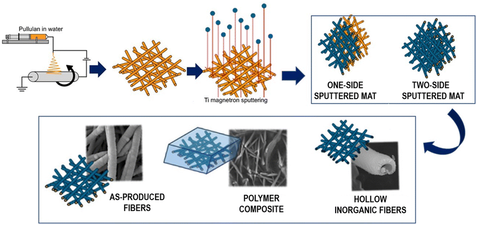 | ||
| Fig. 1 Schematic representation of pullulan electrospinning and Ti magnetron sputtering on the nanofibers for obtaining one-side and two-side sputtered mats. The as-produced fibers were embedded in a thermoplastic matrix for the development of polymer composites and also exploited for the development of hollow inorganic fibers. | ||
The deposition process was designed to coat only one or both faces of the nanofibrous mat and the resulting samples were labelled “one-side sputtered mats” and “two-side sputtered mats”, respectively. We demonstrate the feasibility of removing the polymer material through water solubilization to obtain hollow fibers and compare this process with a conventional thermal degradation protocol. We also demonstrate the possibility of embedding TiOx-based fibers in a thermoplastic polymer matrix to prepare an organic–inorganic composite, where the hollow fibers may create empty channels.
Pullulan was chosen in this work as a sacrificial fiber material since it is a commercially available natural polysaccharide highly soluble in water29 and easily electrospun with a scalable and environmentally friendly process. Moreover, water solubility can be exploited in the stage of polymer template removal, eliminating the need for energy-consuming processes, such as the thermal degradation of the polymer and the use of organic solvents.30 In addition to their biobased nature and water solubility, pullulan nanofibers have an extensive temperature range of applicability,31 as evidenced by a temperature of thermal degradation above 300 °C (Fig. S1†), significantly higher than the temperature reached by the substrate during the magnetron sputtering process, which is a few tens of degrees above room temperature. The as-spun electrospun nanofibers were characterized by a bead-free, regular, and smooth morphology, featuring a similar mean diameter for the upper face of the mat (0.54 ± 0.15 μm) and the lower face in contact with the grounded metal plate during electrospinning (0.45 ± 0.08 μm) (Fig. 2a).
 | ||
| Fig. 2 Macroscopic views and SEM-FEG imaging of the two mat faces (upper one on the left and lower one on the right) of the as-spun mat (a), one-side sputtered mat (b), and two-side sputtered mat (c). AFM characterization of the as-spun mat (scale bar 100 nm) (d) and the Ti-sputtered face of the one-side sputtered mat (scale bar 200 nm) (e). | ||
Following Ti sputtering, a significant change in the color (from white to dark grey) of the exposed face of the mat was observed, together with a notable increase in the diameter of fibers exposed to the Ti target in both one-side (Fig. 2b, fiber diameter: 1.53 ± 0.30 μm) and two-side (Fig. 2c, fiber diameter of the upper face: 1.35 ± 0.15 μm and fiber diameter of the lower face: 1.29 ± 0.7 μm) sputtered mats, highlighting the repeatability of the deposition process (see also fiber diameter distribution reported in Fig. S2†). Moreover, the mean diameter of the fibers on the non-sputtered face of the one-side sputtered mat (0.45 ± 0.10 μm) remained practically the same as the value obtained for the as-spun mats. The result demonstrated the incomplete penetration of Ti atoms through the entire thickness of the mat during one-side sputtering, as also confirmed by the white color of the non-sputtered face of the mat (Fig. 2b). A significant increase in the root mean square roughness of the surface of the fibers from 1.35 nm (Fig. 2d) to 25.70 nm (Fig. 2e) was also observed by AFM measurements after the sputtering processes. The results of EDS analysis, reported in Table S1,† agreed with the SEM-FEG results, confirming the absence of Ti atoms in the as-spun mat and on the non-sputtered surface of the one-side sputtered mat.
The presence of Ti atoms was evident on the coated faces of both the one-side and two-side sputtered mats, constituting approximately 60–70 atomic%, along with a notable decrease in atomic carbon concentration. The significant reduction in carbon concentration occurred alongside a less substantial decrease in oxygen atomic concentration, suggesting partial oxidation of the sputtered Ti. The presence of the inorganic component in one-side and two-side sputtered mats was also confirmed by TGA results (Fig. 3a). The analysis was performed in a N2 atmosphere to minimize oxidation of metal Ti atoms present in the sputtered coating, which would increase the residual weight. Nevertheless, a distinctly different trend was observed for the two-side sputtered mat compared to the other two samples in the temperature range of 430 °C–700 °C. Indeed, a slight increase in weight was detected for this sample, likely attributable to the occurrence of the nitriding of titanium during the measurement. Indeed, although generally performed at higher temperatures (i.e., 800 °C–1100 °C),32,33 the formation of titanium nitride (TiN) in pure nitrogen shows a highly negative standard free energy over a broad temperature range, and it has been demonstrated to occur through the chemisorption of nitrogen on the surface of Ti independently of the nitriding method.34 As expected, the morphology of the as-spun nanofibers was completely lost after the TGA analysis (Fig. 3b), while no significant differences can be observed between the one-side (Fig. 3c) and two-side sputtered mats (Fig. 3d), whose residues were mainly composed of nanotubes.
 | ||
| Fig. 3 (a) TGA curves of the as-spun mat, one-side sputtered mat, and two-side sputtered mat. SEM-FEG images of the residues of the pullulan mat (b), one-side sputtered mat (c) and two-side sputtered mat (d) after TGA in a N2 atmosphere. XPS analysis of the two-side sputtered mat (e–h): widescan spectrum collected at a take-off angle of 45° (e); narrow scan spectra of the C 1s region (f); Ti 2p region (g); O 1s region (h) (XPS measurements were carried out on both faces of the mat and the same results were obtained). XRD pattern of the two-side sputtered mat (i). Resistivity measurements performed on the surface of the two-side coated electrospun mats (similar results were obtained for both faces) (j). | ||
The XPS analysis of the two-side sputtered mat showed the presence of carbon (peak centered at ∼285 eV), oxygen (peak centered at ∼532 eV), and titanium (peak centered at ∼460 eV) on the outer surface of the two-side sputtered mat (widescan in Fig. 3e). Their atomic abundances calculated from the areas under each peak were: C = 60.7 ± 3.0%, O = 30.4 ± 1.5%, and Ti = 8.9 ± 0.44%. From the study of each atomic region, further information can be derived. Curve fitting of the C1s peak (Fig. 3f) revealed the presence of adventitious carbon, typically found on the surface of most samples exposed to air. Its presence on insulating surfaces provides a convenient reference for calibrating binding energies. A value of 285 eV was assigned to this hydrocarbon contamination. Alongside this component, there were other peaks due to the presence of carbon atoms with higher oxidation states (centred at 286.5, 288, 289.5, and 291 eV), hypothesized to originate from a mixture of pullulan, acidic products, and carbonates resulting from degradation processes. The titanium region (445–470 eV) in Fig. 3g showed signals derived from titanium in different oxidation states. Due to spin–orbit coupling, each Ti2p peak was split into two signals (Ti2p3/2 and Ti2p1/2). Curve fitting of these signals produced different peaks attributable to Ti2p3/2 (centred at about 454.1, 456.2, and 459.1 eV) and Ti 2p1/2 (centred at about 459.6, 462.2, and 464.6 eV). The binding energies associated with these contributions were in agreement with the presence of metallic Ti (454.1 eV), Ti2O3 (456.2 eV), and TiO2 (459.1 eV) (Fig. 3g). The relative atomic abundance of the three titanium oxidation states, calculated from the area under the respective peaks, was as follows: 3.8 ± 0.2% metallic Ti, 45.1 ± 2.2% titanium in Ti2O3, and 51.1 ± 2.5% titanium in TiO2. The O1s region (Fig. 3h) showed, in addition to components derived from oxygen bonded to carbon atoms due to pullulan, acidic products, and carbonates, a clear component (centred at ∼530.4 eV) due to the combination of oxygen with titanium, resulting in an O/Ti ratio of 1.51, close to the O/Ti ratio of 1.69 calculated based on the relative abundance of the components of the Ti2p3/2 peak.
The investigation of the fiber crystallographic structure using XRD (Fig. 3i) highlighted the presence of the typical triplet (35°, 38°, and 40°), indicative of a hexagonal close-packed crystal structure, suggesting the presence of the α-Ti crystalline phase.35,36 However, minor peaks at 53° and 63° were undetectable. The highest intensity of the peak at 38° might suggest a preferential (002) orientation of the titanium crystals.36 Notably, the crystalline form of titanium dioxide was not detected, as evidenced by the absence of its representative peaks (25° and 37° for anatase and 28° and 42° for rutile),37 indicating that the titanium oxide phase layer was predominantly amorphous, as expected since the substrate was heated at a relatively low temperature during the sputtering deposition. Finally, the wide signal between 10° and 25° was attributed to the amorphous phase of the pullulan nanofibers’ substrate. Taken together, the EDS, XPS and XRD analyses suggest the presence of crystalline metal Ti, in a low percentage, and of amorphous Ti2O3 and TiO2 in the sputtered coating. The presence of Ti oxides was further confirmed by the resistivity measurements through the four-point probe method (Fig. 3j), highlighting a decrease in resistivity with increasing temperature, which suggests a semiconductor-like behavior. As temperature rises, more electrons are excited from the valence band to the conduction band, promoting conduction by the increased availability of intrinsic charge carriers (electrons and vacancies).38 TiO2 is a typical n-type semiconductor,39 diverging from pure Ti metal, which would typically exhibit enhanced resistivity with increased thermal energy. Recently, Ti2O3 thin films deposited via magnetron sputtering were reported to show a gradual decrease in resistivity with increasing temperature,40 similar to the behaviour observed for the two-side coated mats. Therefore, the n-type semiconductor properties of the mats were influenced by the formation of both TiO2 and Ti2O3 in the sputtered coating. EDS analysis of the cross-sections of both one-side and two-side sputtered mats qualitatively showed that Ti atoms penetrated about 100 μm into the mats under the given magnetron sputtering conditions. The Ti concentration decreased with depth (Fig. 4), indicating that the two-side sputtered mat likely consists entirely of fibers coated with Ti/TiOx, although the fibers in the inner region may be only partially coated. This observation is further supported by SEM imaging of the cross-sections. In the case of the one-side sputtered mat, a noticeable charging effect is observed in the cross-section area containing non-coated fibers. In contrast, no charging effect is seen in the two-side sputtered mats, confirming that all fibers in the latter are coated with Ti/TiOx.
 | ||
| Fig. 4 EDS analysis along the thickness of the one-side and two-side coated mats. | ||
Hollow structures were generated from two-side sputtered mats using two distinct methods, as illustrated in Fig. 5a and b: thermal degradation and water solubility of the pullulan template.
 | ||
| Fig. 5 Schematic representation of (a) pullulan thermal degradation and (b) solubilisation procedures for the obtainment of hollow structures. SEM-FEG (c–f) and TEM imaging (g–j) of hollow structures obtained from two-side sputtered mats after the pullulan thermal degradation (c, d, g and h) or solubilisation procedure (e, f, i and j). | ||
The first procedure was carried out in air and it led to nanotubes (Fig. 5c and d) showing a comparable morphology to those obtained after TGA in nitrogen (Fig. 3d). The thermal degradation of the polymeric template was conducted in air to prevent the presence of organic pullulan residue at the end of the measurement. However, in air, fiber oxidation inevitably occurred, resulting in the formation of hollow structures mostly consisting of TiOx. More interesting was the second method, water solubilization, which involved soaking the two-side sputtered mat in distilled water. The successful removal in water of the polymeric template was confirmed by comparing the TGA curves of the mats before and after pullulan solubilization (Fig. S3†). Indeed, the characteristic degradation step of pullulan was not detected for the hollow nanostructures, indicating the complete removal of the polymeric template. SEM-FEG and TEM analyses of the fibers after pullulan solubilization showed hollow structures (Fig. 5e, f, i and j) with a wall thickness of 0.32 ± 0.18 μm, similar to those obtained through thermal degradation (Fig. 5c, d, g and h), with the added advantages of a more effective preservation of the nanostructures’ chemical composition and an estimated higher sustainability of the whole process (ESI†).
The presence of the TiO2 phase, likely retained in its original amorphous state due to the absence of additional thermal treatments, makes the resulting hollow structures suitable for various applications.41 Their disordered atomic arrangement enhances light harvesting in the visible and near-infrared regions.42 Additionally, amorphous TiO2 serves as an excellent substrate for surface-enhanced Raman scattering (SERS) due to its characteristic energy band structure.43 Furthermore, it functions as a protective coating for photoelectrodes in photo-induced water splitting applications, preventing corrosion. The structural disorder of amorphous TiO2 reduces the energy required for oxygen vacancy formation, increasing the abundance of these vacancies compared to crystalline TiO2. These vacancies act as deep donors, facilitating hole transport and enhancing conductivity.41,44
Finally, to further explore the application of the obtained TiOx-based hollow fibers, two-side sputtered mats were incorporated as fillers into a thermoplastic polyamide 6,6 matrix using a simple room-temperature mat impregnation process.
SEM images (Fig. 6a–d) confirmed the successful integration, with fibers uniformly coated with a thin polymer layer that preserved their rough morphology. Cross-sectional analysis showed well-embedded fibers within the matrix, and after water immersion, hollow fibers became clearly visible due to the dissolution of pullulan nanofibers (Fig. 6e–h).
 | ||
| Fig. 6 SEM imaging of the two-side sputtered mat coated with polyamide: top-view (a and b) and cross-section (c and d). SEM imaging of the cross-section of the two-side sputtered mat coated with polyamide after water immersion at different magnifications (e–h). | ||
Conclusions
In summary, we presented an environmentally friendly approach for realizing TiOx-based hollow fiber networks, thanks to the use of a sacrificial template of continuous pullulan nanofibers produced by electrospinning and magnetron sputtering techniques. Compared to the most established methods, the proposed approach offers advantages, particularly in terms of sustainability and scalability. One of the key benefits of this approach is its eco-friendly nature. With respect to the procedures exploiting the electrospinning for the fabrication of sacrificial polymeric templates, our method replaces fossil-based polymers and toxic solvents with a natural polysaccharide and water, respectively, reducing the environmental impact and enhancing the safety and cost-effectiveness of the process. Another significant advantage is the sustainable template removal in water, preventing the use of organic solvents for its dissolution. Additionally, magnetron sputtering eliminates the need for toxic chemical precursors, also preventing waste generation. Moreover, the process is performed at room temperature, further increasing its sustainability.The Ti-sputtered fibers can be extremely attractive for different applications since they can be used as organic–inorganic fibrous networks, as hollow titanium oxide fibers, or as structural/functional fibrous elements in composites with thermoplastic or thermoset matrices, where they can generate empty channels. Moreover, the potential applications of the produced hollow titanium oxide fibers can extend to fields such as light-harvesting devices and protective coatings for photoelectrodes in photo-induced water splitting applications.
Author contributions
Anna Liguori: Conceptualization, data curation, formal analysis, investigation, validation, visualization, supervision, and writing – original draft; Luca Lorenzetti: data curation, formal analysis, investigation, validation, visualization, and writing – original draft; Giulia Bianchi: data curation, formal analysis, investigation, and visualization; Federico Morini: investigation; Chiara Gualandi: investigation and writing – review and editing; Andrea Zucchelli: conceptualization and writing – review and editing; Massimiliano Bestetti: investigation, methodology, validation, and writing – review and editing; Antonino Pollicino: data curation, methodology, formal analysis, investigation, validation, visualization, and writing – original draft; Carla Martini: conceptualization, methodology, validation, visualization, supervision, and writing – review and editing; Maria Letizia Focarete: conceptualization, data curation, funding acquisition, methodology, supervision, validation, resources, and writing – review and editing.Data availability
The additional data supporting this article have been included as part of the ESI.†Conflicts of interest
There are no conflicts to declare.Acknowledgements
The authors acknowledge Professor Tobias Cramer, from the Department of Physics and Astronomy “Augusto Righi”, University of Bologna, for his support with AFM characterization. This research was funded by the Italian Ministry of University and Research (MUR), through PRIN2020 2020833Y75 and the Department of Excellence Program (L. 232 01/12/2016), by the National Recovery and Resilience Plan (NRRP), Mission 04 Component 2 Investment 1.5 – NextGenerationEU, Call for tender n. 3277 dated 30/12/2021, Award Number: 0001052 dated 23/06/2022, and by Fondazione CarisBo (project #18668 “Tecnologie avanzate per il controllo e lo sviluppo di molecole innovative per la salute”).References
- X. Wang, C. Drew, S. H. Lee, K. J. Senecal, J. Kumar and L. A. Samuelson, Nano Lett., 2002, 2, 1273–1275 CrossRef.
- A. Greiner and J. H. Wendorff, Angew. Chem., Int. Ed., 2007, 46, 5670–5703 CrossRef PubMed.
- J. Xue, T. Wu, Y. Dai and Y. Xia, Chem. Rev., 2019, 119, 5298–5415 CrossRef PubMed.
- D. Li, J. T. McCann, Y. Xia and M. Marquez, J. Am. Ceram. Soc., 2006, 89, 1861–1869 Search PubMed.
- M. Hedayati, E. Taheri-Nassaj, A. Yourdkhani, M. Borlaf, J. Zhang, M. Calame, T. Sebastian, S. Payandeh and G. J. Clemens, J. Am. Ceram. Soc., 2020, 40, 1269–1279 Search PubMed.
- G. George, T. Senthil, Z. Luo and S. Anandhan, Electrospun Polymers and Composites Ultrafine Materials, High Performance Fibres and Wearables Woodhead Publishing Series in Composites Science and Engineering 2021, pp. 689–764 Search PubMed.
- D. Li and Y. Xia, Nano Lett., 2004, 4, 933–938 CrossRef.
- J. T. McCann, D. Li and Y. Xia, J. Mater. Chem., 2005, 15, 735–738 RSC.
- L. Li, X. Liu, G. Wang, Y. Liu, W. Kang, N. Deng, X. Zhuang and X. Zhou, Chem. Eng. J., 2021, 421, 127744 CrossRef.
- C. Wang, X. Tan, J. Yan, B. Chai, J. Li and S. Chen, Appl. Surf. Sci., 2017, 396, 780–790 CrossRef.
- H. Duan, Y. Wang, S. Li, H. Li, L. Liu, L. Du and Y. Cheng, J. Mater. Sci., 2018, 53, 3267–3279 Search PubMed.
- J. Wang, J. Hou, M. Ellis and A. S. Nain, New J. Chem., 2013, 37, 571–574 RSC.
- Y. Gu, D. Chen, X. Jiao and F. Liu, J. Mater. Chem., 2007, 17, 1769–1776 RSC.
- S. Zhan, D. Chen, X. Jiao and S. Liu, J. Colloid Interface Sci., 2007, 308, 265–270 CrossRef CAS PubMed.
- X. Li, Q. Qian, W. Zheng, W. Wei, X. Liu, L. Xiao, Q. Chen, Y. Chen and F. Wang, Mater. Lett., 2012, 80, 43–45 Search PubMed.
- Z. Du, L. Guo, T. Zheng, Q. Cai and X. Yang, Ceram. Int., 2019, 45, 23975–23983 Search PubMed.
- H. Wu, D. Kong, Z. Ruan, P. C. Hsu, S. Wang, Z. Yu, T. J. Carney, L. Hu, S. Fan and Y. Cui, Nat. Nanotechnol., 2013, 8, 421–425 CrossRef CAS PubMed.
- I. M. Szilágyi and D. Nagy, J. Phys.:Conf. Ser., 2014, 559, 012010 CrossRef.
- G. Di Pompo, A. Liguori, M. Carlini, S. Avnet, M. Boi, N. Baldini, M. L. Focarete, M. Bianchi, C. Gualandi and G. Graziani, Biomater. Adv., 2023, 144, 213231 CrossRef CAS.
- G. Pagnotta, G. Graziani, N. Baldini, A. Maso, M. L. Focarete, M. Berni, F. Biscarini, M. Bianchi and C. Gualandi, Mater. Sci. Eng., C, 2020, 113, 110998 CrossRef CAS PubMed.
- N. N. M. Jafri, J. Jaafar, F. Aziz, W. Norharyati, W. Salleh, N. Yusof, M. H. D. Othman, M. A. Rahman, A. F. Ismail, R. A. Rahman and W. Khongnakorn, Membranes, 2022, 12, 342 CrossRef CAS.
- J. Kim, Polymers, 2022, 14, 4942 CrossRef CAS PubMed.
- S. W. Choi, J. Y. Park, C. Lee, J. G. Lee and S. S. Kim, J. Am. Ceram. Soc., 2011, 94, 1974–1977 CrossRef CAS.
- A. Katoch, J. H. Kim and S. S. Kim, ACS Appl. Mater. Interfaces, 2014, 6, 21494–21499 Search PubMed.
- S. Jana, A. K. Debnath, P. Veerender, J. Bahadur, J. Kishor, A. K. Chauhan and D. Bhattacharya, Thin Solid Films, 2022, 763, 139608 Search PubMed.
- C. Guillén and J. Herrero, Thin Solid Films, 2017, 636, 193–199 CrossRef.
- M. Bartolewska, A. Kosik-Kozioł, Z. Korwek, Z. Krysiak, D. Montroni, M. Mazur, G. Falini and F. Pierini, Adv. Healthcare Mater., 2025, 14, 2402431 Search PubMed.
- S. S. Zargarian, A. Zakrzewska, A. Kosik-Kozioł, M. Bartolewska, S. A. Shah, X. Li, Q. Su, F. Petronella, M. Marinelli, L. De Sio, M. Lanzi, B. Ding and F. Pierini, Nanotechnol. Rev., 2024, 13, 20240100 Search PubMed.
- K. Y. Lee, L. Jeong, Y. O. Kang, S. J. Lee and W. H. Park, Adv. Drug Delivery Rev., 2009, 61, 1020–1032 CrossRef CAS PubMed.
- J. W. Huh, H. W. Jeon and C. W. Ahn, Curr. Appl. Phys., 2017, 17, 1401–1408 CrossRef.
- C. Gualandi, A. Zucchelli, M. F. Osorio, J. Belcari and M. L. Focarete, Nano Lett., 2013, 13(11), 5385–5390 CrossRef CAS PubMed.
- C. Li, X. Lv, J. Chen, X. Liu and C. Bai, Int. J. Refract. Met. Hard Mater., 2015, 52, 165–170 CrossRef CAS.
- A. S. Bolokang and M. J. Phasha, Int. J. Refract. Met. Hard Mater., 2010, 28, 610–615 CrossRef CAS.
- G. E. Totten and D. S. MacKenzie, Heat Treating of Nonferrous Alloys, ASM Handbook, 2016 Search PubMed vol. 4E.
- F. B. Kværndrup, F. B. Grumsen, S. Kadkhodazadeh, K. V. Dahl, M. A. J. Somers and T. L. Christiansen, Mater. Charact., 2021, 180, 111435 CrossRef.
- D. M. Tshwane, R. Modiba and A. S. Bolokang, Mater. Today Commun., 2020, 24, 101168 CrossRef CAS.
- Z. Tang, J. Zhang, Z. Cheng and Z. Zhang, Mater. Chem. Phys., 2023, 77, 314–317 Search PubMed.
- A. Yildiz, S. B. Lisesivdin, M. Kasap and D. Mardare, J. Non-Cryst. Solids, 2008, 354, 4944–4947 CrossRef CAS.
- L. A. Dobrzański, M. M. Szindler, M. Szindler, K. Lukaszkowicz and A. Drygała, Arch. Metall. Mater., 2016, 61, 833–836 Search PubMed.
- W. Wang, J. He and Y. Yao, Int. J. Appl. Ceram. Technol., 2025, 22, e14857 CrossRef CAS.
- S. Sun, P. Song, J. Cui and S. Liang, Catal. Sci. Technol., 2019, 9, 4198 RSC.
- X. Xu, S. Wen, Q. Mao and Y. Feng, ACS Appl. Mater. Interfaces, 2018, 10, 39238 CrossRef CAS PubMed.
- H. Bao, H. Zhang, G. Liu, Y. Li and W. Cai, Langmuir, 2017, 33(22), 5430 CrossRef CAS PubMed.
- H. F. Lu, F. Li, G. Liu, Z. G. Chen, D. W. Wang, H. T. Fang, G. Q. Lu, Z. H. Jiang and H. M. Cheng, Nanotechnology, 2008, 19, 405504 CrossRef PubMed.
Footnotes |
| † Electronic supplementary information (ESI) available: Experimental section: materials; fabrication of pullulan electrospun mats; magnetron sputtering of Ti on electrospun mats; characterization of Ti-sputtered electrospun mats; development of hollow structures and their characterization; embedding of electrospun mats coated on two sides in a polyamide matrix. Results of TGA characterization of the as-spun pullulan mat; fiber diameter distribution; EDS analysis; thermogravimetric analysis of the hollow structures obtained from pullulan water solubilisation; estimation of the overall environmental impact. See DOI: https://doi.org/10.1039/d4nr04710a |
| ‡ These authors equally contributed. |
| § Current address: Justus Liebig University Giessen, Institute of Inorganic and Analytical Chemistry, Heinrich-Buff-Ring 17, D-35392 Giessen, Germany. |
| This journal is © The Royal Society of Chemistry 2025 |