
Spatially resolved optoelectronic puddles of WTe2–2D Te heterostructure†
Thi Uyen
Tran‡
a,
Ngoc Thanh
Duong‡
b,
Dae Young
Park
 c,
Jaeuk
Bahng
a,
Hai Phuong
Duong
b,
Van Dam
Do
d,
Mun Seok
Jeong
c and
Seong Chu
Lim
*ab
c,
Jaeuk
Bahng
a,
Hai Phuong
Duong
b,
Van Dam
Do
d,
Mun Seok
Jeong
c and
Seong Chu
Lim
*ab
aDepartment of Smart Fab. Technology, Sungkyunkwan University (SKKU), Suwon 16419, Republic of Korea
bDepartment of Energy Science, Sungkyunkwan University (SKKU), Suwon 16419, Republic of Korea. E-mail: seonglim@skku.edu
cDepartment of Physics, Hanyang University, Seoul 04763, Republic of Korea
dDepartment of Electrical and Computer Engineering, Sungkyunkwan University (SKKU), Suwon 16419, Republic of Korea
First published on 10th April 2025
Abstract
Two-dimensional (2D) semiconductors have attracted significant scientific interest because of their optical properties. Their applications in optoelectronic devices can be further expanded by combining them to form heterostructures. We characterized a WTe2–2D Te heterostructure through local probing of the photocurrent with respect to the magnitude, phase, and position. Photocurrent generation within the device is divided into distinct regions: photo-thermoelectric effects occur solely at the 2D Te–Au junction area, PV-dominant effects at the 2D–WTe2 interface, and thermoelectric-to-photovoltaic crossover effects at the WTe2–2D Te overlap area. These different photocurrents cannot be fused into a single domain because each area is governed by different generation mechanisms, which depend on the location of the device. The power dependence of each photocurrent type also varies within the device. Our results indicate that careful material selection and device structure design, based on the electronic, optical, and thermal properties of the channel materials, are essential to avoid forming different optoelectronic puddles that could counteract each other within a single device.
New conceptsThe key operating principle of photocurrent generation in two-dimensional heterojunctions is the photovoltaic (PV) effect. Most heterojunctions rely solely on the PV effect to achieve energy band alignments and generate a strong built-in electric field. However, our research reveals that incident light introduces heat to the channel in addition to the PV effect, creating a temperature gradient. Combined with the semiconductor's significant Seebeck coefficient, this gradient contributes to the overall performance of the device. The device comprises domains contributing to different types of photoresponses, called optoelectronic puddles. We found that by applying a source–drain bias (Vds) and a gate-source bias (Vgs), we enhanced the extraction of both PV and photo-thermoelectric (PTE) carriers, thereby modulating the device's band structure and thermoelectric properties. In the WTe2–2D Te heterostructure, the typical photo-thermoelectric (PTE) effect dominates near the ohmic contact (Te/Au), while the WTe2/Te junction is PV-dominant due to its weak Schottky nature. Under bias conditions, the photoresponses became spatially dispersive, shifted in position, and exhibited different power dependencies. Notably, this phenomenon is observable across a broad range of wavelengths, from visible to near-infrared. These findings provide new insights into photocurrent generation mechanisms in van der Waals heterostructures. |
Introduction
Two-dimensional (2D) semiconductors, including phosphorene and various transition metal dichalcogenides (TMDs), have gained significant attention because of their unique geometries, which preserve their bulk properties even at the nanometer scale.1–4 These materials have been extensively investigated for their optical, electrical, and optoelectronic applications.5–8 An individual semiconductor has unique characteristics that originate from its specific crystalline atomic structure.9–11 Furthermore, different 2D crystals can be assembled beyond single crystals to form van der Waals (vdWs) heterostructures. Heterostructures display the best ingredients in one structure to improve the performance of 2D material-based devices and serve as a platform for exploring new physical phenomena.12–17Optical devices are commonly fabricated by constructing heterostructures with different layered materials. Among them, solar cells, light-emitting diodes, and broadband photodetectors have been studied, demonstrating the versatility of the heterostructure design in diverse applications across the photonic spectrum. When strategically combined into heterostructures, the unique properties of 2D materials facilitate efficient solar energy conversion, precise control over the emitted light wavelengths, and extended spectral responses.14,17,18 In optoelectronic devices, built-in potential arising from the mismatch in Fermi energy is a key device feature. Compared to Si devices, where the dopant type and concentration control the built-in potential,18 2D heterostructures employ mismatched Fermi levels from the constituent layers and produce a large depletion region with a short carrier transport length in a vertical structure.19 Fabrication results in multiple junctions in devices, such as metal–semiconductor and semiconductor–semiconductor junctions. Unexpected potential barriers form in devices without carefully tuning the junction's Fermi levels or band structures.20 Furthermore, gate and source–drain bias have been controlled to enhance device performance. The biases vary the junction barrier height and the carrier concentration of the semiconducting channel, alter the material properties, and introduce different light detection mechanisms rather than the initially designed photovoltaic (PV). For example, MoS2, WSe2, and ReS2 have been incorporated into various optical devices. However, they showed metal–insulator transitions under gate modulation.21–23 Previous results indicated that built-in potentials with differences in magnitude and direction constitute the heterostructure, and different metallicities can locally occupy the channel.24 The device performance can be improved by homogenizing the local potential variations and coordinating the photocurrent in the same direction. The local potential can be developed from the Fermi level mismatch, thermoelectrics by local laser heating, light-induced polarization, and ionization.25–28 In addition, local variations in the carrier concentration can occur in the heterostructure, which subsequently develops into local potential puddles in the devices. The development of optoelectronic puddles would not be recognizable in many cases because they result from impurities or unexpectedly occur from device operation, as stated above. Therefore, the existence and correlation between them need to be better acknowledged. In this regard, proving the photocurrent on a microscopic scale can provide insights into how diverse local domains of photocurrents are present in the channel, how much their responses are controllable using the back-gate bias, and how capable we are of commensurating them to produce an in-phase photocurrent. Investigation and an understanding of these issues are in high demand to discover and advance the functionalities of optoelectronic devices. For instance, many applications have an array of pixels for light detection and target recognition, inside which photoelectric properties need to be uniform and repetitive.29–32 Maximizing the desired performance from each pixel and orchestrating it is feasible when we understand formations and prevention of puddles.
In this study, we fabricated a 2D Te field-effect transistor (FET) using two different electrodes, Au and 1T’ WTe2. Thus, the device consists of two junctions: semiconductor–metal and semiconductor–semimetal junctions. In our device of WTe2–2D Te–Au, near the ohmic junction between 2D Te and Au, the photothermoelectric (PTE) is dominant, whereas the WTe2–2D Te junction is PV dominant because of its Schottky nature in the junction. The stacked area of WTe2–2D Te is switchable from PV to PTE, depending on the biases. Moreover, even with the alternation of Vds and Vgs, it is difficult to achieve both a single optoelectronic domain and uniform photocurrent distribution. Thus, a channel open to the incident light simultaneously produces different types of photocurrents. Designing optoelectronic devices using 2D semiconducting heterojunctions requires careful consideration of the puddle types, current flow in the puddles, and their distributions, because the puddles sometimes flow the current in opposite directions. Prior to design, an investigation of the nature and distribution of puddles is required. Our observations provide insights into the heterostructure, where the homogenization of photocurrent puddles is crucial for enhancing the devices’photoelectric performance. Our exploration lays the groundwork for selecting and enhancing the system's homogeneous photocurrent.
Results and discussion
Fig. 1a shows the schematic of a hybrid WTe2–2D and Te–Au field-effect transistors on a highly hole-doped silicon substrate covered with a 300-nm SiO2 layer as the gate dielectric. Two-dimensional (2D) Te flakes were synthesized via a hydrothermal method14,33 and transferred onto a SiO2/Si substrate. A mechanically exfoliated semimetallic 1T′ WTe2 flake was stacked on top of a 2D Te flake to form a heterojunction. X-ray diffraction patterns of WTe2 and 2D Te were shown in Fig. S1 (ESI†). Thicknesses of WTe2 and 2D Te were measured via atomic force microscopy (AFM) are 9.5 and 17.8 nm, respectively (Fig. S2, ESI†). The metal electrodes were defined using electron-beam lithography (EBL), followed by the deposition of Cr/Au (10/70 nm) using a thermal evaporator (see Experimental section). An optical image of the device is shown in Fig. 1b, in which the red and blue lines represent WTe2 and 2D Te, respectively. The optical properties of the semimetallic 1T′ WTe2/2D Te heterojunction were characterized using the Raman spectra shown in Fig. 1c. Notably, the Raman modes of WTe2 (A12 and A15) were completely suppressed at the heterojunction, which was further confirmed by the Raman mapping shown in Fig. 1d. The intensity map of A12 Raman mode of WTe2 is shown in Fig. 1d. Details of the other Raman modes of WTe2 and 2D Te can be found in the ESI,† Fig. S3. The severe contrast of the Raman signals between pure WTe2 on SiO2 and WTe2 on 2D Te indicates a possible charge transfer between these two materials,34,35 which was further clarified in electrical measurements.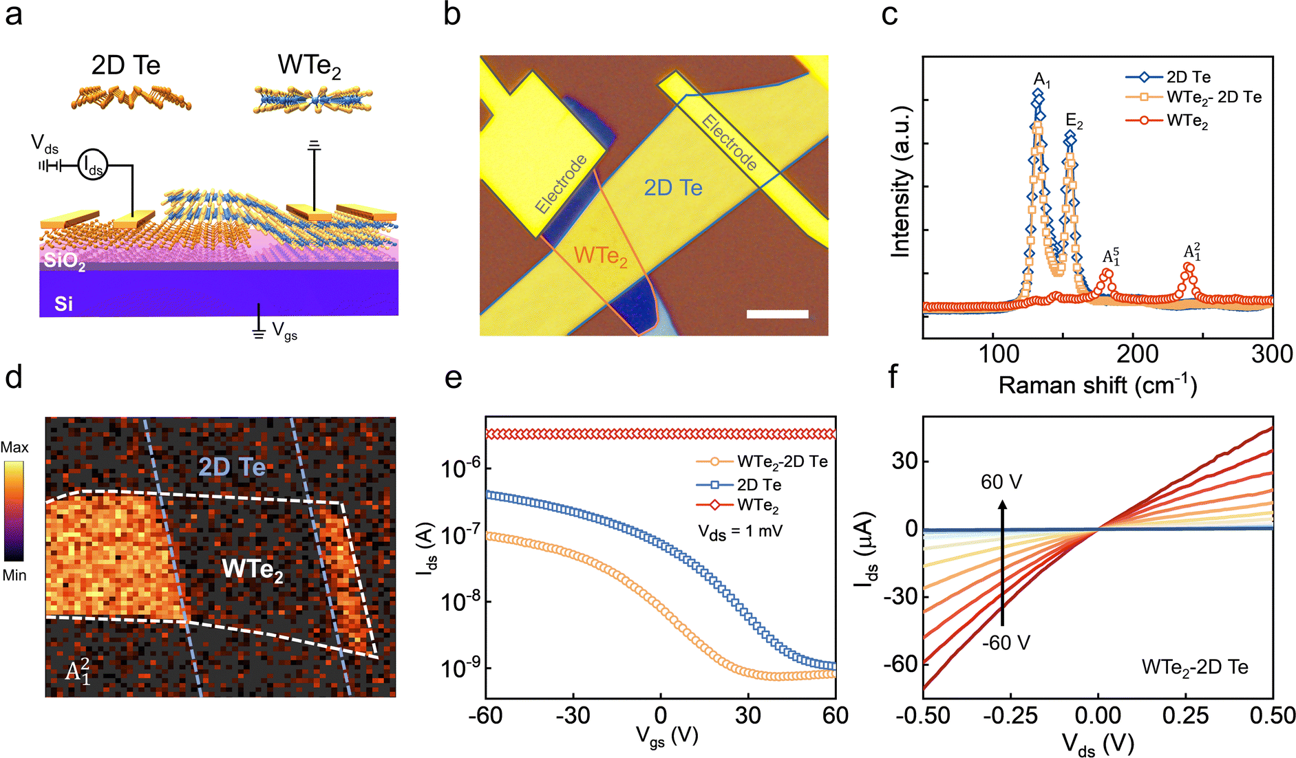 | ||
| Fig. 1 (a) Schematic and (b) optical image of the WTe2–2D Te heterostructure device. (c) Raman spectra of WTe2, 2D Te, and WTe2/2D Te heterojunction. (d) Raman intensity maps for A15 mode of WTe2 and WTe2 on 2D Te. (e) Transfer curves of the WTe2, 2D Te, and WTe2–2D Te devices obtained in the dark at room temperature. (f) Output curves of WTe2–2D Te heterojunction device. | ||
Fig. 1e shows the electrical properties of WTe2, 2D Te, and WTe2–2D Te FETs. The WTe2 device exhibited typical semimetal behavior without gate modulation, whereas the 2D Te device exhibited p-type behavior. The transfer curve of the hybrid WTe2–2D Te FET exhibited p-type transport characteristics. The threshold voltage of the heterojunction device shifted toward a lower voltage compared with that of 2D Te alone, signifying electron transfer from 1T WTe2 to 2D Te. We estimated the amount of electron transfer by comparing the hole concentrations of each 2D Te and WTe2–2D Te heterojunction using a parallel capacitor model, which is expressed as n = C(Vgs − Vthres)/q, where n, C, Vgs, Vthres, and q are the carrier concentration, capacitance of SiO2, gate voltage, threshold voltage, and electrical charge, respectively.36 The majority hole carrier concentration is estimated to be 8.5 × 1012 cm−2 and 6.7 × 1012 cm−2 at Vgs = −60 V for the former and latter, respectively. Thus, Δn is 1.8 × 1012 cm−2. The output curves of the WTe2–2D Te FET are sublinear, as shown in Fig. 1f, whereas the metal contacts of both WTe2 and 2D Te are linear (Fig. S4 for WTe2 and 2D Te FETs, ESI†). Thus, the junction created by WTe2–2D Te is predicted to be non-ohmic, which contributes to the photovoltaic current under illumination.
We characterized the photoelectric behavior of the devices using a homemade system as shown in Fig. S5 (ESI†). The magnitude, phase (photocurrent direction), and position of the photocurrent depend on the electrical, thermoelectric, and thermal properties of the channel materials, which can be further regulated using Vds and Vgs. In the case of the phase, if the photocurrent flows from the source to the drain electrode, the phase is zero degrees. In the reverse direction, the phase is 180 degrees. We can map the local potential profile resulting from various causes, including Fermi level mismatch, laser-induced heating, and impurity ionization, by analyzing the magnitude, direction, and position of the photocurrent. Furthermore, the drain–source and gate-source modulations present the alternation of these three parameters inside the channel.
Under Vgs = 40 V and Vds = 0 V, the magnitude, location, and phase maps of the photocurrent obtained using our system are shown in Fig. 2a and b, respectively. The photocurrent map of the device shown in Fig. 2a is classified in three regions, that is, (1), (2), and (3). In Fig. 2b, the phase map shows that the photocurrents in regions (1) and (3) flow in the same direction from the drain to the source electrode, whereas the photocurrent in region (2) flows in the opposite direction from the source to the drain electrode. First, we characterized the photocurrent observed in the 2D Te channel in regions (1) and (2). 2D Te is a narrow-bandgap semiconductor, with Eg = 0.35 eV.14,15,37 In addition, it is a good thermoelectric material with a high Seebeck coefficient (S) and low thermal conductivity (k), which can promote the PTE effect in regions (1) and (2) under local laser irradiation.26 Near the drain electrode (Au) in region (1), both the PV current (IPV), owing to the depletion region and the PTE current (IPTE) from the local laser heating indicate the same direction.33 PV prevails over the depletion region only, although PTE can sustain outside the depletion region with a temperature gradient (∇T) along the channel. The linear proportionality of Ids−Vds in the ESI,† Fig. S4c (ESI†) indicates that the contact between the 2D Te and Cr/Au electrode is ohmic with no depletion region. Hence, thermally excited hole carriers by the laser diffuse out from hot to cold area and forges IPTE, which is expressed as IPTE = VPTE/R = −S▽T/R, where VPTE, R, S, ∇T are photothermal voltage, resistance, Seebeck coefficient, and temperature gradient. Therefore, the photocurrent in region (1), 2D Te–Au junction, can be attributed to the typical PTE effect in 2D Te. The photocurrent in region (2), 2D Te–WTe2 junction, was much higher than that in region (1), as plotted in Fig. 2a and c. The photocurrent along a red dashed line in Fig. 2a is extracted for each Vgs value and shown in Fig. 2c. Another type of photocurrent is suspected in region (2) in the same direction as IPTE. Considering the slightly sublinear output curves in Fig. 1f and the energy band bending of 2D Te at the junction with WTe2 shown in Fig. 2d, an IPV would be generated in region (2). To further clarify PV at the junction of WTe2 and 2D Te, we performed Kelvin probe force microscopy (KPFM) with details in ESI,† Fig. S6. The work functions of WTe2, 2D Te, and their heterojunction were estimated to be 4.32, 4.65, and 4.5 eV, respectively. As a result, the accumulation mode was formed at the junction, playing a crucial role in the examination of direction and magnification of PV.
 | ||
| Fig. 2 (a) Intensity and (b) phase maps of the photocurrent from WTe2/2D Te heterojunction at Vds = 0 V and Vgs = 40 V. The mapping images were obtained with a laser power of 5 μW. The scale bar signifies 5 μm. (c) Photocurrent intensity along red dashed lines in Fig. 2a with respect to Vgs (−40, −20, 0, 20, and 40 V). (d) A schematic for the energy band and flow direction of IPTE and IPV in the heterojunction. (e) Schematic for PTE in the heterojunction with respect to Vgs. (f) Seebeck coefficients of 2D Te and WTe2 as a function of Vgs. | ||
It is interesting to investigate the photocurrent behavior of the WTe2–2D Te heteroarea in region (3). PV is commonly responsible for photocurrent generation in semiconductor–semimetal junctions.24–27 Nevertheless, we excluded this possibility in region (3). If it were to be a built-in potential, it would develop in the vertical direction between 2D Te and WTe2 but remain constant laterally in region (3). Hence, region (3) is inherently insufficient for charge separation except at the edge. In addition, the photocurrent inside region (3) flowed in the opposite direction to IPV in region (2), as evidenced by the phase map in Fig. 2b. We attribute the photocurrent in the WTe2–2D Te heteroarea to the PTE, which originates from a different Seebeck coefficient, as demonstrated in Fig. 2e. The dissimilar thermoelectric properties are further confirmed in Fig. 2f. In Fig. 2e, the grayscale of the crimson indicates the different Seebeck coefficient in region (3). The Seebeck coefficient of 2D Te is quite sensitive to the back gate bias, although that of WTe2 remains intact. The gray scale is modulated by back gate bias, as indicated by an arrow.
The 2D Te layer is expected to exhibit a high VPTE due to its high S, whereas the WTe2 layer is expected to have a low VPTE due to its low S. This photothermal voltage gradient could encourage IPTE streaming from the 2D Te layer to the WTe2 layer. We monitored the photocurrent as a function of Vgs to further verify the PTE in the heterojunction in region (3), as shown in Fig. 2c and Fig. S7 (ESI†). The photocurrent map at various Vgs values revealed the modulation of the spatial extent, gradient, and strength of the local potential formed by laser-induced heating effects. As shown in Fig. 2c, the photocurrent in region (3) increases with Vgs, owing to the growth of VPTE between the 2D Te and WTe2 layers with Vgs. Our characterization of the Seebeck coefficient as a function of Vgs for 2D Te and WTe2 is shown in Fig. 2f and Fig. S8 (ESI†). Both show positive S, indicating that holes are the majority carriers. The Mott relation describes that the Seebeck coefficient is inversely proportional to the conductance (G), S ∼ 1/G.38 Therefore, STe increased with Vgs, whereas SWTe2 remained constant with Vgs. Larger difference in S between 2D Te and WTe2 results in stronger VPTE in the heterojunction, which is expressed as VPTE = −(STe − SWTe2)▽T. Therefore, IPTE enhances the heterojunction with increasing Vgs. Unlike previous studies on the ReS2–2D Te heterojunction,33 the small difference in the Seebeck coefficient between ReS2 and 2D Te is insufficient to activate the photothermoelectric effect between ReS2 and 2D Te layers. Therefore, the photocurrent in the ReS2–2D Te junction is mainly controlled by the photothermoelectric current from 2D Te alone. Moreover, in Fig. 2c, the IPTE is stronger in region (3) than in region (1). This is because the S of 2D Te in region (3) is expected to be enhanced compared to S of 2D Te in region (1), owing to electron doping upon contact with WTe2, as shown in Fig. 1c–e. Moreover, we characterized the power-dependent photocurrents in regions (1) and (3), as shown in ESI,† Fig. S9. Following the power law, the exponential parameter, α = 0.79 and α = 1.25, are extracted from regions (1) and (3), respectively. These values indicate the superior efficiency of PTE in the WTe2–2D Te overlapped area compared to that of 2D Te alone. Our results imply that in addition to channel materials, the channel structure plays a significant role in enhancing the photo-responses of 2D materials.
In addition to the modulation of Seebeck coefficient using the back gate bias to control PTE in region (3), a significant enhancement of PTE is observed when the device is exposed to laser with the wavelength of 1064 nm. The results are available in ESI,† Fig. S10. Furthermore, the fast response time of PTE, approximately 1.2 μs, is examined with various wavelengths 450 nm, 811 nm, and 1064 nm, as shown in Fig. S11 (ESI†).
We observed an IPTE pit, indicated by an arrow, at the boundary between regions (2) and (3), as shown in Fig. 2c. This is because, at the junction, different photocurrents flow in opposite directions, as shown in Fig. 2d, resulting in a photocurrent pit. Our investigation proved that our device consisted of a few domains, inside which distinctive photocurrents were generated. The existence of domains can degrade device performance when the device is exposed to global illumination. Alternatively, leveraging the unique characteristics of each type of photocurrent allows the device to adaptively operate. The impact of Vds on the selection and enhancement of the homogeneous photocurrent in the system is subsequently characterized.
The photocurrent domains can be greatly productive and expand in size when the photocurrent flows in the same direction as Vds. Otherwise, they become infertile and shrink. In addition to the variation in the preexisting photocurrent domains, the application of Vds contributes to the additional photoconductive current (IPC). With an ohmic contact, we should obtain a constant IPC, indicated by a red line, regardless of the location in the channel, which is proportional to Vds, as shown in Fig. 3a. However, the distribution of IPC along the channel becomes inhomogeneous when the channel is accompanied by local photovoltaic and photothermoelectric effects, as shown in Fig. 3b and c (see Fig. S12 for more details, ESI†). We must note the photocurrent dispersed with increasing distance.
 | ||
| Fig. 3 The effect of Vds on the photocurrent that arises from the (a) ohmic contact-, (b) Schottky contact-, and (c) thermoelectric device. | ||
We applied Vds = 2 V to investigate the nature of the photocurrent in region (2), which also remarkably suppressed IPTE in regions (1) and (3). As shown in Fig. 4a, b, and Fig. S13 (ESI†), there is a strong photocurrent only in region (2), and the current is highly subject to Vgs compared to the other regions. The enhancement is significant at Vgs = −40 V, followed by a dramatic decrease as Vgs increases (details are shown in Fig. S13, ESI†). In this region, IPV + IPTE can flow together along Vds. The depletion of IPV is anticipated to occur with increasing Vgs, attributed to the decrease in the built-in potential with Vgs, as depicted in Fig. 4c. In contrast, unlike IPV, IPTE is expected to increase with Vgs, as indicated by the STe − Vgs relation shown in Fig. 2f. The line profile in Fig. 4b is magnified and plotted in Fig. 4d. The shrinking photocurrent with increasing Vgs between 4 and 10 μm shows that a local built-in potential drives IPV. The PV region continuously shrinks with increasing Vgs and it sustains only near the junction between 2D Te and WTe2, at approximately 4–6 μm. Over 6 μm (marked by an arrow in Fig. 4b and d), the photocurrent is considerably small but relatively uniform at Vgs = 40 V. The photocurrent obtained at Vgs = 40 V and Vds = 2 V was assumed to be Ipc rather than IPV and IPTE. Under this bias scheme, IPV and IPTE were effectively suppressed due to the reduction of built-in potential and Seebeck coefficient, while IPC remained due to the applied Vds. Even distribution of photocurrent along the channel reflects the behaviour of IPC. The line profile of the current along the channel in Fig. 4b between 6 to 10 μm at Vgs = 40 V resembles the one in Fig. 3a with Vds.
 | ||
| Fig. 4 (a) Photocurrent intensity map of the WTe2–2D Te interface at Vds = 2 V and Vgs = −40 V. The mapping images were obtained with a laser power of 5 μW. The scale bar signifies 5 μm. (b) and (d) Photocurrent intensity along the red dashed line in Fig. 4a with respect to Vgs (−40, 0, and 40 V). (c) Schematic for energy band and flow directions of different photocurrents in the heterostructure at Vds = 2 V and the modulation of built-in potential (Vbi) with Vgs at the junction of 2D Te and WTe2. | ||
In region (3), the gate-dependent photocurrent within the decreases as Vgs increases. When Vds = 2 V, the thermoelectric voltage contribution is eliminated in this region. One peculiar behavior of the photocurrent inside region (3) is the growing photocurrent at a distance between 0 and 4 μm. The gradual increase of photocurrent in region (3) is considered to be a manipulation of IPV caused by Vds.
Then, we applied Vds = −2 V to the device to investigate the PTE effect in regions (1) and (3). With this bias, IPTE can be selectively animated, whereas IPV can be unanimated. Our analysis of the photocurrent behavior with different Vgs values is shown in Fig. 5a–c and Fig. S14 (ESI†). With the assistance of Vds, the photocurrent along the channel exhibited the PTE trait, as shown in Fig. 5d, increasing with increasing Vgs. This behavior is outstanding only in region (1). By excluding region (1), the effect of gate modulation on IPTE is weak, implying that the photothermoelectric generation is weak. In addition, in region (2), the photocurrent is proportional to the distance from x = 5 μm (i.e., it increases as the laser moves toward the drain electrode because of Vds). Based on the flat energy band shown in Fig. 3a, the applied Vds increases the band slope and enhances the separation of electron–hole carriers. Consequently, the photocurrent density should be constant and independent of the position. However, as shown in Fig. 3c, when IPTE is coupled with IPC, the photocurrent (IPTE + IPC) is position-dependent, which agrees with the results shown in Fig. 3c.
 | ||
| Fig. 5 Photocurrent intensity maps of the WTe2–2D Te heterostructure at Vds = −2 V at different Vgs (−40, 0, and 40 V) values: (a) −40 V, (b) 0 V, and (c) 40 V. The mapping images were obtained with a laser power of 5 μW. The scale bar signifies 5 μm. (d) Photocurrent intensity along the red dashed lines with respect to the channel length. | ||
In addition, it is important to note the position-dependent photoresponses in Fig. 4 and 5, which result of the incorporation of Vds into either the photovoltaic or photothermoelectric devices, as shown in Fig. 3. However, these are distinguishable using gate-bias dependence. In Fig. 4, a negative gate-bias dependence is observed (i.e., the photocurrent decreases as Vgs increases), although the opposite behavior is presented in Fig. 5. In Fig. 4, the negative gate bias dependence is responsible for the photovoltaic mechanism, whereas in Fig. 5, the positive gate bias dependence is ascribed to the photothermoelectric cause. The alternating appearance of either a positive or negative trend depending on Vgs implies that on a 2D Te channel with metal and semimetal junctions, both photovoltaic and photothermoelectric properties coexist and each region exerts a phenomenon favorable for the specific bias condition.
Compared to other semimetal–semiconductor heterostructures that exhibit only PV, WTe2–2D Te heterojunction also reveals PTE arising from the different thermoelectric performance of WTe2 and 2D Te layer. In this structure, PV + PTE coexist, which is unable to be observed in a single structure of WTe2 and 2D Te (Table 1). Notably, the dominant mechanism can be effectively controlled by applying biases, allowing the selection of different photocurrent types for specific design purposes (see Table 1 in ESI† for the summary of photocurrent mechanisms in each bias condition).
Conclusions
Diverse 2D layer materials and their combined structures have been fabricated and investigated to enhance and control the photovoltaic properties from the mismatch of the Fermi levels. The structures demonstrated not only PV but also PTE and their hybrids. These different types of photoresponses are inherent to the device and feature when the conditions are met. Therefore, the devices exhibited different photocurrents under incident light. To enhance device performance, their identification and local distribution must be characterized on a microscopic scale, and subsequent homogenization of the photocurrent types is essential. Therefore, the materials and device structure should be carefully selected to minimize the formation of photocurrent puddles. Fabrication of the photodetectors with a single and uniform photoelectric domain prerequisites multimodal characterization of electronic, optical, and thermal behavior of the channel materials. Understanding and regulating the interplay among various materials properties and their dependences on the external bias is another aspect of 2D material photodetector that a future study must seek for, with potential significant implications.Experimental methods
Synthesis of 2D tellurene
The 2D Te flakes were synthesized using a standard hydrothermal method.14,33 First, 104 mg of sodium tellurite (Na2TeO3) and 3.1 g of polyvinylpyrrolidone (PVP) were dissolved in 30 mL of deionized water under vigorous magnetic stirring at room temperature. Then, 3.2 mL of ammonium hydroxide solution and 1.7 mL of monohydrate hydrazine were added to the solution. The homogeneous solution was transferred to a Teflon-lined stainless-steel autoclave and kept in an oven at 180 °C for 20 h. The resulting silver-gray products were centrifuged at 5000 rpm for 5 min and washed thrice with deionized water to remove the residuals. The precipitated product was preserved in distilled water until subsequent fabrication.Device fabrication
2D Te flakes on distilled water were spin-coated onto a SiO2(300 nm)/Si substrate. Subsequently, the mechanically exfoliated WTe2 flake, from commercially available bulk crystals and 2D semiconductors, was stacked on the 2D Te flake to form a heterostructure using a common dry-transfer method. EBL was utilized to pattern the electrodes. Finally, Cr/Au (10/70 nm) was thermally deposited as a metal contact for the WTe2 and 2D Te, and the silicon substrate served as a back-gate electrode.Characterization
Raman scattering measurements were performed using an NTEGRA spectra instrument (NT-MDT) equipped with a 532 nm wavelength-laser at room temperature. AFM measurements were performed using the DFM mode of an AFM SPA400 (SEIKO). The electrical properties were characterized using a Keithley-4200 SCS. The photocurrent was measured using a self-designed photocurrent mapping system (Fig. S5, ESI†).Author contributions
T. U. T and N. T. D. wrote the draft of the manuscript. T. U. T, N. T. D., and S. C. L. revised the manuscript. S. C. L. conceived and supervised the project. J. B. and H. P. D. support experiments and data analysis. T.U.T and N.T.D contributed equally to this work. V. D. D. and D. Y. P. contributed to KPFM and XRD measurement in the revised manuscript, respectively.Data availability
The data supporting this article have been included as part of the ESI.†Conflicts of interest
There are no conflicts to declareAcknowledgements
This research was funded by the National Research Foundation of Korea (NRF) (Grant Number: RS-2024-00357405 and RS-2024-00433138). N.T.D acknowledges the BrainPool (BP) Program, National Research Foundation of Korea (NRF) (Grant Number: RS-2023-00264072).Notes and references
- S. A. Thomas, J. Cherusseri and D. N. Rajendran, ACS Appl. Electron. Mater., 2024, 6, 4321–4335 CrossRef CAS.
- Y. Kong, S. M. Obaidulla, M. R. Habib, Z. Wang, R. Wang, Y. Khan, H. Zhu, M. Xu and D. Yang, Mater. Horiz., 2022, 9, 1253–1263 RSC.
- S. Anna Thomas and J. Cherusseri, J. Energy Chem., 2023, 85, 394–417 CrossRef CAS.
- S. M. Obaidulla, A. Supina, S. Kamal, Y. Khan and M. Kralj, Nanoscale Horiz., 2024, 9, 44–92 RSC.
- F. Zhou, Z. Zhou, J. Chen, T. H. Choy, J. Wang, N. Zhang, Z. Lin, S. Yu, J. Kang, H.-S. P. Wong and Y. Chai, Nat. Nanotechnol., 2019, 14, 776–782 CrossRef CAS PubMed.
- S. Wang, X. Liu and P. Zhou, Adv. Mater., 2022, 34(48), 2106886 CrossRef CAS PubMed.
- S. Aftab and H. H. Hegazy, Small, 2023, 19(18), 2205778 CrossRef CAS.
- Z. Cheng, T. Zhao and H. Zeng, Small Sci., 2022, 2(1), 2100051 CrossRef CAS PubMed.
- G. Qiu, C. Niu, Y. Wang, M. Si, Z. Zhang, W. Wu and P. D. Ye, Nat. Nanotechnol., 2020, 15, 585–591 CrossRef CAS PubMed.
- S.-Y. Xu, Q. Ma, H. Shen, V. Fatemi, S. Wu, T.-R. Chang, G. Chang, A. M. M. Valdivia, C.-K. Chan, Q. D. Gibson, J. Zhou, Z. Liu, K. Watanabe, T. Taniguchi, H. Lin, R. J. Cava, L. Fu, N. Gedik and P. Jarillo-Herrero, Nat. Phys., 2018, 14, 900–906 Search PubMed.
- D. Kim, K. Park, J. H. Lee, I. S. Kwon, I. H. Kwak and J. Park, Small, 2021, 17(10), 2006310 CrossRef CAS PubMed.
- K. S. Novoselov, A. Mishchenko, A. Carvalho and A. H. Castro Neto, Science, 2016, 353(6298), aac9439 CrossRef CAS PubMed.
- N. T. Duong, J. Lee, S. Bang, C. Park, S. C. Lim and M. S. Jeong, ACS Nano, 2019, 13, 4478–4485 CrossRef CAS PubMed.
- T. U. Tran, D. A. Nguyen, N. T. Duong, D. Y. Park, D. H. Nguyen, P. H. Nguyen, C. Park, J. Lee, B. W. Ahn, H. Im, S. C. Lim and M. S. Jeong, Appl. Mater. Today, 2022, 26, 101285 CrossRef.
- J. Chen, T. Zhang, J. Wang, L. Xu, Z. Lin, J. Liu, C. Wang, N. Zhang, S. P. Lau, W. Zhang, M. Chhowalla and Y. Chai, Sci. Adv., 2022, 8(23), eabn3837 CrossRef CAS PubMed.
- W. Zhuang, Z. Chen and X. Wang, Adv. Phys. X, 2022, 7(1), 2034529 Search PubMed.
- S. M. Young and C. L. Kane, Phys. Rev. Lett., 2015, 115, 126803 CrossRef.
- Z. Zhu, Y. Zou, W. Hu, Y. Li, Y. Gu, B. Cao, N. Guo, L. Wang, J. Song, S. Zhang, H. Gu and H. Zeng, Adv. Funct. Mater., 2016, 26, 1793–1802 CrossRef CAS.
- Y. Shao, R. Jing, S. H. Chae, C. Wang, Z. Sun, E. Emmanouilidou, S. Xu, D. Halbertal, B. Li, A. Rajendran, F. L. Ruta, L. Xiong, Y. Dong, A. S. McLeod, S. S. Sunku, J. C. Hone, J. Moore, J. Orenstein, J. G. Analytis, A. J. Millis, N. Ni, D. Xiao and D. N. Basov, Proc. Natl. Acad. Sci. U. S. A., 2021, 118(48), e2116366118 CrossRef CAS.
- Q. Wang, J. Zheng, Y. He, J. Cao, X. Liu, M. Wang, J. Ma, J. Lai, H. Lu, S. Jia, D. Yan, Y. Shi, J. Duan, J. Han, W. Xiao, J.-H. Chen, K. Sun, Y. Yao and D. Sun, Nat. Commun., 2019, 10, 5736 CrossRef CAS PubMed.
- S. Song, A. Yoon, S. Jang, J. Lynch, J. Yang, J. Han, M. Choe, Y. H. Jin, C. Y. Chen, Y. Cheon, J. Kwak, C. Jeong, H. Cheong, D. Jariwala, Z. Lee and S.-Y. Kwon, Nat. Commun., 2023, 14, 4747 CrossRef CAS.
- B. Datta, J. Vaidya, S. Ghatak, R. Dhingra, R. Mondal, J. Jesudasan, A. Thamizhavel and M. M. Deshmukh, Appl. Phys. Lett., 2021, 119(13), 133501 CrossRef CAS.
- X. Li, Y. Wei, Z. Wang, Y. Kong, Y. Su, G. Lu, Z. Mei, Y. Su, G. Zhang, J. Xiao, L. Liang, J. Li, Q. Li, J. Zhang, S. Fan and Y. Zhang, Nat. Commun., 2023, 14, 111 CrossRef CAS PubMed.
- M. Du, X. Cui, H. H. Yoon, S. Das, M. G. Uddin, L. Du, D. Li and Z. Sun, ACS Nano, 2022, 16, 568–576 CrossRef CAS PubMed.
- Y. Huang, H. Yu, W. Gao, P. Wen, Z. Liu, H. Wang, M. Zhang and J. Li, J. Mater. Chem. C, 2023, 11, 5045–5055 RSC.
- C. Li, Z. Wu, C. Zhang, S. Peng, J. Han, M. He, X. Dong, J. Gou, J. Wang and Y. Jiang, Adv. Opt. Mater., 2023, 11(22), 2300905 CrossRef CAS.
- C. Zhang, S. Peng, J. Han, C. Li, H. Zhou, H. Yu, J. Gou, C. Chen, Y. Jiang and J. Wang, Adv. Funct. Mater., 2023, 33(40), 2302466 CrossRef CAS.
- N. Dihingia, G. A. Vázquez-Lizardi, R. J. Wu and D. Reifsnyder Hickey, J. Chem. Phys., 2024, 160(9), 091101 CrossRef CAS.
- J. Fu, C. Nie, F. Sun, G. Li, H. Shi and X. Wei, Sci. Adv., 2024, 10(7), eadk8199 CrossRef PubMed.
- J. Fu, Z. Guo, C. Nie, F. Sun, G. Li, S. Feng and X. Wei, Innovation, 2024, 5, 100600 Search PubMed.
- H. Jiang, J. Fu, J. Wei, S. Li, C. Nie, F. Sun, Q. Y. S. Wu, M. Liu, Z. Dong, X. Wei, W. Gao and C.-W. Qiu, Nat. Commun., 2024, 15, 1225 CrossRef CAS PubMed.
- J. Zhou, Y. Wang, M. Xia, Y. Chen, D. Huang and X. Zhang, Nano Lett., 2024, 24, 9658–9665 CrossRef CAS PubMed.
- T. U. Tran, J. Bahng, X. D. Dang, S. Oh, H. P. Duong, S. S. Kang, H. M. Yu, W. Sakong, M. Kim, H.-S. Choi, J. Baik, M. S. Jeong and S. C. Lim, Nano Energy, 2022, 102, 107720 CrossRef CAS.
- N. T. Duong, S. Bang, S. M. Lee, D. X. Dang, D. H. Kuem, J. Lee, M. S. Jeong and S. C. Lim, Nanoscale, 2018, 10, 12322–12329 RSC.
- M. Bruna, A. K. Ott, M. Ijäs, D. Yoon, U. Sassi and A. C. Ferrari, ACS Nano, 2014, 8, 7432–7441 CrossRef CAS.
- Z. Gao, F. Tao and J. Ren, Nanoscale, 2018, 10, 12997–13003 RSC.
- N. T. Duong, J. Lee, S. Bang, C. Park, S. C. Lim and M. S. Jeong, ACS Nano, 2019, 13, 4478–4485 CrossRef CAS.
- C. Yang, G. Wang, M. Liu, F. Yao and H. Li, Nanomaterials, 2021, 11, 2688 CrossRef CAS.
- G. Qiu, S. Huang, M. Segovia, P. K. Venuthurumilli, Y. Wang, W. Wu, X. Xu and P. D. Ye, Nano Lett., 2019, 19, 1955–1962 CrossRef CAS PubMed.
- C. Garcia, N. R. Pradhan, D. Rhodes, L. Balicas and S. A. McGill, J. Appl. Phys., 2018, 124(20), 204306 CrossRef.
- M. Du, X. Cui, H. H. Yoon, S. Das, M. G. Uddin, L. Du, D. Li and Z. Sun, ACS Nano, 2022, 16, 568–576 CrossRef CAS PubMed.
- Y. Huang, H. Yu, W. Gao, P. Wen, Z. Liu, H. Wang, M. Zhang and J. Li, J. Mater. Chem. C, 2023, 11, 5045–5055 RSC.
- C. Li, Z. Wu, C. Zhang, S. Peng, J. Han, M. He, X. Dong, J. Gou, J. Wang and Y. Jiang, Adv. Opt. Mater., 2023, 11(22), 2300905 CrossRef CAS.
- C. Zhang, S. Peng, J. Han, C. Li, H. Zhou, H. Yu, J. Gou, C. Chen, Y. Jiang and J. Wang, Adv. Funct. Mater., 2023, 33(40), 2302466 CrossRef CAS.
Footnotes |
| † Electronic supplementary information (ESI) available: Fig. S1–S13. See DOI: https://doi.org/10.1039/d5nh00027k |
| ‡ T. U. T. and N. T. D. contributed equally to this work. |
| This journal is © The Royal Society of Chemistry 2025 |