DOI:
10.1039/D5NA00611B
(Paper)
Nanoscale Adv., 2025,
7, 7598-7605
Ultra-simplified fabrication of all-silver memristor arrays
Received
21st June 2025
, Accepted 25th August 2025
First published on 26th August 2025
Abstract
Brain-inspired neuromorphic computing strives to emulate the human brain's remarkable capabilities, including parallel information processing, adaptive learning, and cognitive inference, while maintaining ultra-low power consumption characteristics. The exponential progress in cloud computing and supercomputing technologies has generated an increasing demand for highly integrated electronic storage systems with enhanced performance capabilities. To address the challenges of tedious fabrication, we innovatively offer a feasible strategy: using weaved silver electrodes combined with in situ formed silver oxide insulating layers to create a high-performance two-terminal memristor array configuration. This memristor possesses a high ON/OFF ratio (above 106) and good durability (200 cycles). Moreover, its innovative weaving-type configuration enables higher integration density while maintaining conformal attachment capability onto the skin. Our ultra-simplified fabrication strategy provides a novel alternative approach for streamlining fabrication processes, enabling the realization of advanced device integration and system miniaturization.
Introduction
Great advancements in computing neuromorphic systems based on memristors have held immense potential owing to their brain-like multilevel parallel information processing capabilities, lower energy consumption, and extended operational lifetime.1–9 The two-terminal memristor, a fundamental component of brain-like neuromorphic computing, operates by altering its resistance value in response to signal excitation. Owing to their precise controllability, low power consumption, multi-level storage capabilities, and a large storage window, memristors hold potential for applications in optical control devices and neural computing, particularly in tasks such as facial classification,10 vision imaging,11 and sparse coding.12 To overcome the limitations of conventional electronic systems, the integration of multifunctional components (e.g. on-chip sources, detectors, and storage devices) into a single microelectronic platform has been identified as a rational and effective strategy for advancing size scaling and intelligentization initiatives in the post-Moore era.13–17 To advance integration and miniaturization, textile-based electronics provide an innovative platform for the development of wearable memristor-based applications, offering a versatile and compact solution for next-generation wearable computing and storage electronics.16–18 Dong et al. designed a non-volatile memory array utilizing crystalline silicon/amorphous silicon (Si/a-Si) core/shell NWs with highly controllable switching threshold voltages.19 However, conventional two-terminal resistive switching memory devices have been limited by their intricate and labor-intensive fabrication processes.20–30 Herein, we present an innovative and remarkably simple strategy for fabricating memristor arrays by weaving surface-oxidized metal wires with pristine metal counterparts, thereby bypassing the complex and time-consuming processes inherent to conventional fabrication approaches. Meanwhile, the miniaturization and space utilization of the device are greatly improved by a crossbar of only 0.5 mm in the silver-wire array. This work establishes a novel paradigm for streamlined fabrication and flexible integration of next-generation electronic devices.
Experimental section
Materials
Commercial Ag wires (D: 30 μm, L: 1 cm) were bought from MSC KOREA, M1536.
Fabrication method
The commercial Ag wires were directly adopted as the electrode of the memristor. Plasmon treatment (70 W, O2 30 sccm) was utilized to oxidize the Ag electrode in situ into Ag2O, serving as the insulating layer of the memristor. Subsequently, the Ag wire with an AgO-oxidized surface was woven with another Ag electrode with a vertical-horizontal cross configuration.
Characterization
Surface morphology was observed under a scanning electron microscope (SEM) (FEI/Quanta 450 FEG). All electrical performance measurements of the memristor were performed on a Keysight B1500A Semiconductor Device Analyzer. The programming pulse voltage was recorded on the Oscilloscope DS1202Z-E.
Results and discussions
Fabrication and characterization of the textile-type memristor
Fig. 1a presents the basic structure scheme of the memristor array, with a magnified schematic diagram of a single unit in the array. A photo illustration of the array is shown in Fig. 1b. This textile-configuration memristor adopts an electrode–insulator–electrode structure, utilizing commercially available Ag wires (30 μm diameter, 1 cm length) as the electrodes. Metal–insulator–metal (MIM) configuration of two-terminal resistive non-volatile memristors is a well-known structure.31,32 According to the conventional procedure for fabricating memristors, the separate processing of the silver oxide insulating layer33,34 complicates the whole preparation process. Alternatively, we ingeniously oxidize the Ag electrode in situ to form the insulating layer of the memristor, silver oxide, achieved through a straightforward plasmon treatment process (70 W, O2 30 sccm, 1–2 minutes). This innovative approach significantly simplifies the fabrication technology, making the process more efficient and accessible. Subsequently, the Ag wire with AgO-oxidized surface were woven with another Ag electrode in a vertical-horizontal cross configuration (Fig. 1c). Actually, metallic oxide generally serves as the insulating layer in the memristors or neuromorphic systems.35 To verify the equivalent effect of our method to traditional atomic layer deposition (ALD) methods, scanning electron microscopy (SEM) was carried out. Fig. 1d shows SEM images of a pristine Ag electrode (left panel), a plasmon-treated Ag electrode (middle panel) and an ALD-deposited Ag2O of Ag electrode (right panel), with the enlarged image presented at the bottom. The morphological similarity between Ag2O formed by plasmon treatment and by ALD demonstrates the rationality of our strategy. The XPS spectra of the Ag electrodes before (pristine, black curve) and after oxidation (blue curve) are presented in Fig. S1. The prominent peak at 530 eV in the oxidized sample's spectrum corresponds to the O 1s orbital, confirming the formation of Ag2O on the electrode surface.
 |
| | Fig. 1 (a) Schematic illustration of an integrated all-silver memristor array. (b) Photo image of a all-silver memristor array. (c) Fabrication process of the memristor array. (d) SEM images of pristine Ag electrode (left panel) and Ag electrode after plasmon treatment (middle panel) and Ag electrode decorated with AgO by ALD (right panel). | |
Electrical performance of the single unit of the memristor
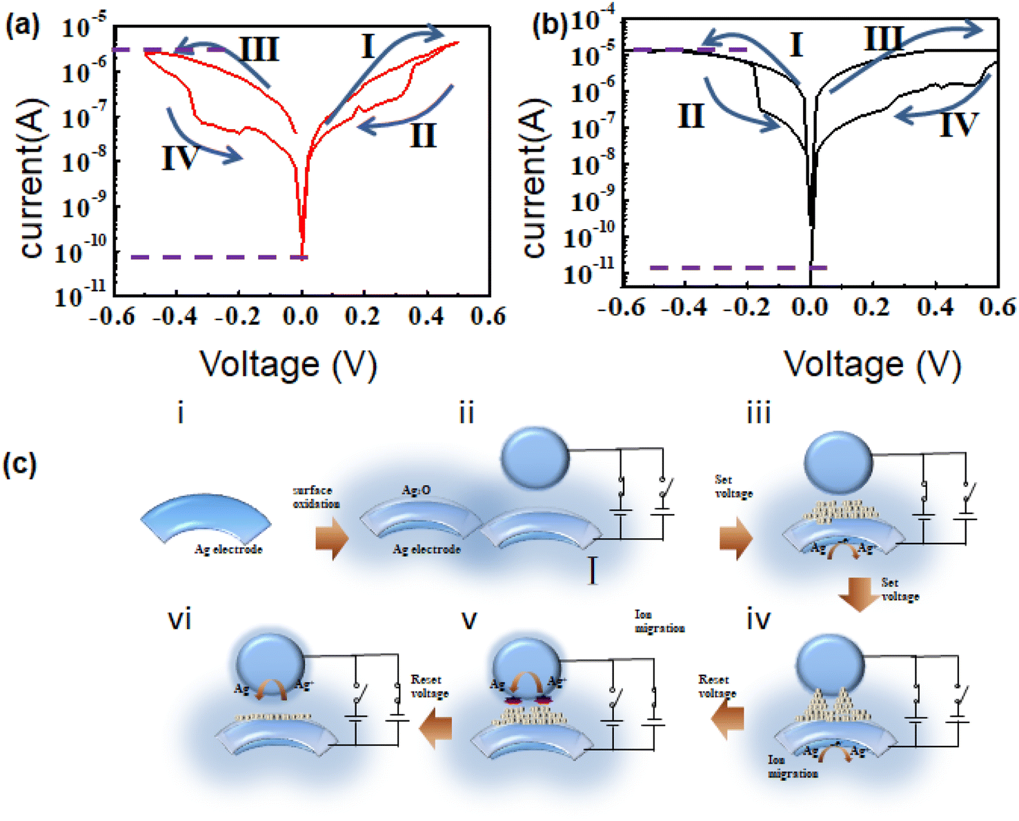
Fig. 2a presents the electrical performance of a single all-silver memristor device. An electroforming process is required to initiate the high initial OFF resistance state for high initial OFF resistance state (107 Ω) by applying a forming voltage of around 0.01 V to activate the bidirectional RS behaviour. Specifically, the maximum nonlinearity achieves a value of 106 under the relatively small voltage of 0.5 V (Fig. S2). Additionally, a steep variation in the resistance from the initial high-resistance state to a low-resistance state occurs under a small positive voltage of about 0.01 V, corresponding to the formation of silver conductive filaments. In particular, the relatively low threshold voltage to open the device indicates low-voltage operation. It also demonstrates that the handy fabrication process does not affect the other electrical properties of the device (ON/OFF ratio, power consumption). The device shows bipolar resistive switching behaviour due to the bipolar transport characteristic of the Ag filament mechanism.36,37 To verify the bidirectional TS character, the sweep path of 0 V → −0.5 V → 0 V → 0.5 V → 0 V was operated on the device. Fig. 2b illustrates the back sweep of the device with no pronounced variation compared to the forward sweep. This is the characteristic of the bipolar transport behavior. Furthermore, it can be observed that whether forward scan or back sweep, the window after the second return to the zero point is larger than the previous one. Due to the accumulation and variation of charges during the reverse scanning process, there is no rectification characteristic.
 |
| | Fig. 2 Memory device characteristics. (a) The typical I–V curve of device under an Icc of 100 μA. (b) The typical I–V curve of the device in back-forward sweep (0 V → −0.5 V → 0 V → 0.5 V → 0 V). (c) The mechanism of the textile-type memristor: (i) the pristine Ag electrode; (ii) Ag electrode undergoes in situ oxidization to form the insulating layer of the memristor; (iii) the application of voltage induces oxidation reaction between the vertically oriented and horizontally oriented silver electrodes, referred to as the “writing” process; (iv) continual increase in the voltage induces Ag filament growth, eventually bridging the bottom and top Ag electrodes; (v), subsequently a converse voltage (referred to as reset voltage) induces an opposite redox reaction (Ag+ reduces to Ag), leading to the dissolution of the conductive filament and a corresponding decrease in conductivity; (vi) continuous negative bias causes complete filament collapse, resetting the device to a high-resistance state, denoted as the “erasing” process. | |
Fig. 2c systematically illustrates the mechanism of the textile-based memristor. As shown in Fig. 2c(i) and (ii), under the 2–3 min plasmon condition, the Ag electrode undergoes in situ oxidization to form the insulating layer of the memristor, silver oxide, in the absence of an applied electrical voltage. The application of voltage induces oxidation reaction between the vertically oriented and horizontally oriented silver electrodes (Ag at the negative potential terminal oxidizes into Ag+), along with a gradual conductivity increment, which is referred to as the “writing” process (as shown in Fig. 2c(iii), corresponding to Fig. 2a(I)). A continual increase in the voltage induces Ag filaments to grow, eventually bridging the bottom and top Ag electrodes (as shown in Fig. 2c(iv), consistent with Fig. 2a(II)). Subsequently a converse voltage (referred to as the reset voltage) induces an opposite redox reaction (Ag+ reduces to Ag), leading to the dissolution of the conductive filament and a corresponding decrease in conductivity (as shown in Fig. 2c(v), corresponding to Fig. 2a(III)). Continuous negative bias causes complete filament collapse, resetting the device to a high-resistance state, denoted as an “erasing” process (Fig. 2c(vi) consistent with Fig. 2a(IV)).
The stability of the devices is a fundamental prerequisite for neuromorphic applications. Fig. S3 shows the nearly identical consecutive I–V performance of the memory device in the initial cycle (red curve), 10 cycles (blue curve), 20 cycles (deep-red curve) and 200 cycles (purple curve). The little deviation with respect to each curve reveals the excellent cycle stability. Furthermore, stability largely depends on relaxation behaviour, which was evaluated by pulse voltage measurements. The endurance of the low-resistance state and the high resistance state was verified by consecutive programming high-voltage pulses and low-voltage pulses, respectively. Fig. S4 illustrates that the device shows over 200 cycles under 2 V voltage pulses (red line, low-resistance state) and 0.3 V read pulses (blue line, high-resistance state) with a pulse width of 100 ms and an interval time of 1 s (1000 ms). Whether in the high-resistance state (HRS) or the low-resistance state (LRS), the retention time can last 50 ms, demonstrating good retention behaviour. Moreover, the device maintains its state over the test time range that the oscilloscope can achieve (60 seconds, 6000 milliseconds). The test provides critical evidence regarding the device's ability to maintain consistent performance, which is essential for reliable operation in neuromorphic systems. The relaxation characteristics of the flexible threshold switching show a relaxation time from 1 ms to 10 s.38Fig. 3a displays the typical current–voltage (I–V) curve of the device under varying compliance currents (yield current).39 The ON/OFF ratio remains nearly consistent as the compliance current varies, although it results in a slight reduction in the resistance window. The maximum allowable compliance current for reliable device operation is approximately 10−3 A. This indicates that the device can maintain stable performance within this current range, which is crucial for ensuring consistent functionality. Besides current, the device also shows high tolerability to a wide voltage range. Fig. 3b presents the typical I–V curves of the device under varied sweep ranges (−1–1 V, −0.8 V–0.8 V, −0.6 V–0.6 V, −0.4 V–0.4 V), verifying that our memristor can tolerate a wide voltage range. Moreover, the comparative analysis between our work and ref. 45 indicates that the handy fabrication process does not affect the other electrical properties of the device (ON/OFF ratio, power consumption).
 |
| | Fig. 3 (a) The typical I–V curve of device under varied compliance currents of 1 μA (blank curve), 0.05 μA (red curve), 0.01 μA (blue curve), 0.005 μA (pink curve). (b) The typical I–V curve of device under varied sweep ranges (−1–1 V, −0.8–0.8 V, −0.6–0.6 V, −0.4–0.4 V). (c and d) I–V sweeps of an Ag/Ag2O/Ag device are shown for (c) a subset of the low-resistance region, and (d) a subset of the high-resistance region. For all curves, only the voltage range from 0.0 V to 0.5 V was considered. (e–g) The performance of devices under different plasmon treatment times: (e) 3 min, (f) 5 min, and (g) 10 min. (h) The performance of devices with different metals: Ag/Ag2O/Pt (red curve), Ag/Ag2O/Ag (violet curve), and Al/Al2O3/Al (blank curve). | |
Fig. S6 illustrates the endurance of the device in the bending state (I–V performance of the memory device in the initial cycle, 10 cycles, 20 cycles, and 200 cycles) at a radius curvature of 38.71 cm−1. The approximate curves indicate that the device exhibits rational applicability in bending and wearable scenarios. This suggests that the device can maintain its functionality and performance even when subjected to mechanical deformation. It is well-known that nonidealities have a significant impact on the training process. The nonlinearity can be defined at voltage Vref as the ratio of the conductance at that voltage to the conductance at half that voltage.40,41 The nonlinearity can be defined as follows:42
| |  | (1) |
where,
G(
Vref) and
G(
Vref/2) are the conductivities at the reference voltage and the conductivity at half the reference voltage, respectively. In this work, we also investigated the effects of
I–
V nonlinearity for our textile-type Ag/AgO/Ag memristor.
40 To realize a wide range of resistance states and to evaluate
I–
V nonlinearity, incremental positive sweeps were utilized to gradually reset the device from the low-resistance state to the high-resistance state.
I–
V curves of two subsets of all achieved states are shown in
Fig. 3c and d. Compared with high-resistance states (in
Fig. 3d), the low-resistance discrete states (in
Fig. 3c) exhibit more linear behavior and exhibit minimal variability in nonlinearity. The effect of different plasmon treatment times on the properties of the devices was also studied.
Fig. 3e–g present performances under different plasmon treatment conditions (1 min, 3 min and 5 min) applied on Ag. It can be observed that the device obtained by 1 min plasmon treatment turns out to have excellent properties. It can be observed that the device obtained by 1 min plasmon treatment turns out to have excellent properties, yet shows degraded properties with 3–5 min plasmon treatment. This ultra-feasibly processable all-silver memristor method can be equivalently applied to other metal electrodes for constructing a memristor.
Fig. 3h presents the
I–
V characteristics of Ag/AgO/Pt (red curve), Ag/AgO/Ag (violet curve), and Al/Al
2O
3/Al (black curve). The typical resistance characteristics and high ON/OFF ratios demonstrate the versatility and effectiveness of our fabrication strategy. A majority of two-terminal non-volatile memristors with a MIM configuration share a metal filament mechanism.
43,44 Ag/Ag
2O/Pt (red curve) and Ag/Ag
2O/Ag (violet curve) adopt an Ag filament mechanism, whereas Al/Al
2O
3/Al (blank curve) utilizes an Al filament mechanism. Therefore, the performance characteristics of the devices vary significantly depending on the electrode and insulating materials. The significantly higher output current observed for Ag/Ag
2O/Pt (red curve), with an Ag filament mechanism, than that for Al/Al
2O
3/Al is consistent with the metal conductivity ordering. Ag is known to have higher electrical conductivity than Al.
45 To further verify the role of Ag electrodes, we also compared
I–
V characteristics of control devices with symmetric non-Ag electrodes Pt/Ag
2O/Pt, demonstrating its lack of resistive switching characteristics (Fig. S5). This can be attributed to the higher reduction potential of Pt electrodes which prevents the electrochemical formation of conductive filaments (compared to Ag
+/Ag).
Principally, the resistive switching behaviors of filamentary memristors are significantly influenced by ion migration and the growth of conductive filaments within the memristive layer. The surface of Ag wire undergoes oxidation, forming a thin layer of Ag2O decorated on the Ag surface.34,46 When an external voltage is applied, Ag undergoes oxidation, transitioning to Ag+ ions, which migrate and form conductive pathways, thereby transitioning the device to a low-resistance state (LRS). Conversely, when the voltage is reversed or removed, these filaments rupture, returning the device to a HRS. The efficiency and stability of ion migration directly impact the device's switching speed, endurance, and reliability. In our previous work,47 we utilized a transmission electron microscope (TEM) as a powerful tool to study the mechanism of memristor devices by implementing the device in a coplanar structure and using the ion beam milling technique. However, this method is restricted in the case of this device because the relatively small contact area between the orthogonal Ag electrodes is restrictive. Based on the resistance-change deviation performance of different metal electrodes in Fig. 3h, combining the inertness characteristic of silver oxide insulating layer without introducing any new mechanism in the resistance, providing the explanation that Ag filament-mechanism is the mechanism of this device.35,48,49 The resistive-switching mechanism can be comprehensively elucidated through systematic analysis of the current–voltage (I–V) characteristics, particularly focusing on the high-resistance state (HRS) during each voltage sweep cycle. To gain deeper insights into the fundamental physical processes governing the resistive switching behavior, the referred equations are expressed as follows:
| |  | (2) |
| |  | (3) |
where,
A represents Richardson's constant,
T denotes the absolute temperature,
ε signifies the dielectric permittivity,
φ corresponds to the barrier height,
k stands for Boltzmann's constant, and
q indicates the electronic charge. The Fowler–Nordheim (FN) tunneling process is predominantly responsible for carrier transport in the high-resistance state during the first voltage sweep. This mechanism suggests that electrons tunnel through the thin insulating barrier under the influence of a strong electric field, which is consistent with the observed behavior in the initial stages of resistive switching. As shown in Fig. S7, ln(
I) exhibits a linear relationship with the square root of
V, which provides strong evidence for the dominance of the thermionic emission (TE) process in carrier transport.
50,51 This is a typical Ag filament rule of reducing filament gap by barrier height reduction through an increasing number of voltage sweeps. We also compared the performance of our work with other typical bipolar memristors, which are listed in
Table 1.
Table 1 The comparison of the performance of different memristor materials
|
|
R
HRS/RLRS |
Positive pulse voltage |
Negative pulse voltage |
Endurance [cycles] |
| Ag/AgO/Pt |
7 × 10⁶ |
0.9 V |
−0.8 V |
200–300 |
| Ag/AgO/Ag |
2 × 10⁶ |
+6 V |
|
200 |
| Al/Al2O3/Al |
104 |
1.19 V |
−1.39 V |
50–100 |
| Cu/Cu2O/Cu |
3 × 10⁴ |
0.5 V |
−0.5 V |
70–120 |
To further verify the reproducibility of the performance, the normal distribution diagram for sensing of 20 identical samples is presented (Fig. S8). As shown in the normal distribution diagram for sensing, the ON/OFF ratio and threshold voltage are respectively concentrated at 1.2 × 10⁶ and 0.012, verifying good reproducibility of our device, which offers reliability for practical applications.
Weaving represents a promising approach for realizing flexible and integrated electronic systems. Yue Liu has proposed textile-type memristor arrays that are mechanically durable to withstand hundreds of bending and sliding deformations, seamlessly unified with sensing, power-supplying, and displaying textiles to form all-textile integrated electronic systems for the new generation of human–machine interactions.52 The advantage of simplified processing, flexible integration, miniaturization and high-efficient space utilization enables the devices to be preferable for highly integrated weave-type devices. On the basis of a single memristor device, a 6 × 8 memristor array has been constructed (this 6 × 8 configuration aligns with the shapes of letters of “L”, “O”, “V”, and “E”). Each pristine silver electrode and each silver electrode decorated with a thin silver oxide insulating layer on the surface (having experienced in situ oxidation treatment) were woven with a vertical-horizontal cross configuration (Ag/Ag2O/Ag) to construct the memristor array. Prior to the testing on the array, a normal distribution diagram of 48 devices, with regards to current distributions across all cells, retention stability, and variation in write/read pulses, is shown in Fig. S9. The current error, write/read pulses variation, and retention time are concentrated at 5.9%, 5.2%, and 5444 ms, respectively. This memristor array, with its well-characterized and consistent performance, can be readily applied to coding applications. The array adopts a loose contact mode, where a 0.5 V voltage was applied between the longitudinal electrode and the transverse electrode. The current is almost 0 because the electrodes are not fully in contact. The longitudinal electrode and the transverse electrode are in a contact state when an external force is applied to each device. The greater the pressure, the larger the contact surface becomes, leading to a reduced resistance and an increase in current. As shown in Fig. 4, the output current distribution shows a given pattern “LOVE”. Meanwhile, only the sensing pixel showed output signals according to the approaching process, indicating no crosstalk in the array. The potential sources of error and limitations are attributed to two aspects: (1) the stability issue of constituent materials compromises device reliability and operational lifespan, and (2) limitations in theoretical modeling necessitate further refinement and optimization of these models to enhance their predictive accuracy and utility in guiding device design.53–55 The linear and continuous conductance regulation,56 as well as the ability to faithfully replicate multimodal perception57 has emerged as a research hotspot (Table 2).
 |
| | Fig. 4 The 2D mapping of the current distribution of memristor array to show an “L”, “O”, “V”, and “E”. | |
Table 2 The comparison of the performance of typical two-terminal memristors
|
|
R
HRS/RLRS |
Positive pulse voltage |
Negative pulse voltage |
Endurance [cycles] |
Ref. |
| Ti/Pt/BP/HfO2/Cu |
105 |
0.9 V |
−0.8 V |
1000 |
11
|
| Gr/SiOx/Gr |
106 |
+6 V |
|
400 |
20
|
| TiN/Al/Ti/Al2O3/TiO2−x/TiN/Al/Ti |
105 |
1.19 V |
−1.39 V |
105 |
21
|
| Al/G-O film/Al |
108 |
0.5 V |
−0.5 V |
∼100 |
22
|
| ITO/MoSe2/Bi2Se3/Ag |
2.83 × 10³ |
−6 V |
6 V |
1000 |
23
|
| Au/NiSAs/N–C/ITO |
103 |
+5 V |
−8 V |
500 |
24
|
| Ti/Pt–MoS2–Ti/Pt |
102 |
2 V |
−2 V |
107 |
25
|
| Cu/pV3D3/MLG/Al |
104 |
−4 V |
4 V |
100 |
26
|
| Ag/MoS2/Ag |
107 |
0.18 V |
|
— |
27
|
| Gr/MoS2−xOx/Gr |
106 |
+0.35 V |
−0.48 V |
2 × 10⁷ |
28
|
| Pt/TiOx/HfO2/Pt |
— |
1.5 V |
−1.5 V |
1.06 × 10³ |
29
|
| Ag/CVD-15-18L-hBN/Au |
1011 |
5 V/2 μs set pulses, 0.1 V/2 μs read pulses |
80![[thin space (1/6-em)]](https://www.rsc.org/images/entities/char_2009.gif) 000 000 |
30
|
| Ag/Ag2O/Ag |
107 |
2 V pulses for LRS, 20 mV pulses for HRS |
200 |
Our work |
Conclusion
The ever-increasing development of integration and miniaturization of advanced electronic devices and systems has imposed much higher requirements for continuously deepening and exploring novel integrated electronic systems. As a summary, we ingeniously offer a considerably simple approach to construct an all-silver memristor without other reagents, featuring a fibre-style configuration to achieve high-level integration and miniaturization. Our all-silver memristor array exhibits a high ON/OFF ratio (above 107) and good durability (200 cycles). This straightforward preparation method significantly enhances processing efficiency while maintaining high performance and integration, holding great practical significance. Additionally, the weaving-type memory array conformally attaches to the skin, offering a novel pathway for the feasible processing and flexible integration of highly integrated and miniaturized memristors. This ultra-feasible and high-efficiency fabrication strategy provides a novel alternative approach for streamlining fabrication processes, enabling the realization of advanced device integration and system miniaturization. It opens a novel avenue for the accessibility of feasible processing and flexible integration of high-level integrated and miniaturized memristors.
Conflicts of interest
The authors declare no competing financial interest.
Data availability
All data generated or analyzed during this study are included in this published article and its SI files. The datasets generated and/or analyzed during the current study are available from the Royal Society of Chemistry publisher and are accessible viahttps://pubs.rsc.org/en/content/articlepdf/2025/NA/D5NA00611B?page=search. See DOI: https://doi.org/10.1039/d5na00611b.
Acknowledgements
We gratefully acknowledge the support by the Research start-up Fund of Jiangsu University (No. 5501110021) provided during the research. We also gratefully acknowledge the waiver of the page charge offered during the submission process.
Notes and references
- A. A. Talin, Y. Li and D. A. Robinson,
et al.
, Adv. Mater., 2023, 35, 2204771 CrossRef PubMed.
- C. W. Lee, C. Yoo and S. S. Han,
et al.
, ACS Nano, 2024, 18, 18635–18649 CrossRef PubMed.
- M. Lanza, F. Hui and C. Wen,
et al.
, Adv. Mater., 2023, 35, 2205402 CrossRef.
- I. Rabiul, S. Yu and V. Gabriel,
et al.
, ACS Nano, 2024, 18, 22045–22054 CrossRef.
- Y. Ren, X. Y. Huang and J. H. Joshua,
et al.
, J. Food Process Eng., 2022, 45, 21873–21885 Search PubMed.
- H. Jiang, Y. C. He and Q. S. Chen,
et al.
, J. Sci. Food Agric., 2020, 101, 3448–3456 CrossRef PubMed.
- H. Teixeira, C. Dias and A. V. Silva,
et al.
, ACS Nano, 2024, 18, 21685–21713 CrossRef.
- X. D. Chen, L. Chen and J. X. Zhou,
et al.
, Nano Lett., 2024, 24, 10265–10274 CrossRef PubMed.
- Y. P. Xia, N. Lin and J. J. Zha,
et al.
, Adv. Mater., 2004, 36, 2403785 CrossRef.
- X. Wang, Y. Lu and J. Zhang,
et al.
, Small, 2021, 17, 2005491 CrossRef PubMed.
- D. Kumar, H. R. Li and U. K. Das,
et al.
, Adv. Mater., 2023, 35, 2300446 CrossRef PubMed.
- P. M. Sheridan, F. Cai and C. Du,
et al.
, Nat. Nanotechnol., 2017, 12, 784–789 CrossRef PubMed.
- B. Sun, Y. Z. Chen and G. D. Zhou,
et al.
, ACS Nano, 2024, 18, 14–27 CrossRef.
- Z. Cao, Y. Liu and B. Sun,
et al.
, Adv. Mater., 2024, 36, 2411659 Search PubMed.
- J. Michel, J. Liu and L. C. Kimerling, Nat. Photonics, 2010, 4, 527–534 CrossRef.
- V. R. Almeida, C. A. Barrios and R. R. Panepucci,
et al.
, Nature, 2004, 431, 1081–1084 CrossRef PubMed.
- Y. A. Vlasov, X. Z. Bo and J. C. Sturm,
et al.
, Nature, 2001, 414, 289–293 CrossRef PubMed.
- S. Wu, F. Zabihi and R. Y. Yeap,
et al.
, ACS Nano, 2023, 17, 1022–1035 CrossRef PubMed.
- Y. Dong, G. Yu and M. C. McAlpine, Nano Lett., 2008, 8, 386–391 CrossRef PubMed.
- J. Yao, J. Lin and Y. H. Dai,
et al.
, Nat. Commun., 2012, 3, 1101 CrossRef PubMed.
- H. Kim, M. R. Mahmoodi and H. Nili,
et al.
, Nat. Commun., 2021, 12, 5198 CrossRef PubMed.
- H. Y. Jeong, J. Y. Kim and J. W. Kim,
et al.
, Nano Lett., 2010, 10, 4381–4386 CrossRef PubMed.
- Y. Wang, J. Yang and Z. P. Wang,
et al.
, Small, 2019, 15, 1805431 CrossRef PubMed.
- H. X. Li, Q. X. Li and F. Z. Li,
et al.
, Adv. Mater., 2024, 36, 2308153 CrossRef PubMed.
- B. S. Tang, H. Veluri and Y. D. Li,
et al.
, Nat. Commun., 2022, 13, 3037 CrossRef PubMed.
- B. C. Jang, H. Seong and J. Y. Kim,
et al.
, 2D Mater., 2015, 2, 044013 CrossRef.
- X. W. Feng, Y. D. Li and L. Wang,
et al.
, Adv. Electron. Mater., 2019, 5, 1900740 CrossRef.
- M. Wang, S. H. Cai and C. Pan,
et al.
, Nat. Electron., 2019, 1, 130–136 CrossRef.
- S. Pi, C. Li and H. Jiang,
et al.
, Nat. Mater., 2019, 14, 35–39 Search PubMed.
- S. C. Chen, M. R. Mahmoodi and Y. Shi,
et al.
, Nat. Electron., 2020, 3, 638–645 CrossRef.
- E. J. Yoo, M. Lyu and J. H. Yun,
et al.
, Adv. Mater., 2015, 27, 6170–6175 CrossRef.
- C. H. Wang, W. He and Y. Tong,
et al.
, Small, 2017, 13, 1603435 CrossRef PubMed.
- B. K. Keshav, S. S. Saha and S. Debroy,
et al.
, ACS Appl. Electron. Mater., 2024, 6, 1007–1017 CrossRef.
- M. Fujimoto, H. Koyama and Y. Nishi,
et al.
, Appl. Phys. Lett., 2007, 91, 223504 CrossRef.
- A. Wedig, M. Luebben and D. Y. Cho,
et al.
, Nat. Nanotechnol., 2016, 11, 67–74 CrossRef PubMed.
- K. Krishnan, T. Tsuruoka and C. Mannequin,
et al.
, Adv. Mater., 2016, 28, 640–648 CrossRef.
- C. X. Wu, T. W. Kim and T. L. Guo,
et al.
, Adv. Mater., 2017, 29, 1602890 CrossRef PubMed.
- D. Joksas, E. Wang and N. Barmpatsalos,
et al.
, Adv. Sci., 2022, 9, 2105784 CrossRef.
-
Z. M. Tang, R. J. Zhao, L. K. Luoet al., Constraints-Aware Training (CAT), Albuquerque, United States, 2023, pp. 20–26 Search PubMed.
- C. Sung, S. Lim and H. Kim,
et al.
, Nanotechnology, 2018, 29, 115203 CrossRef.
- M. Kobayashi, Int. J. Neural Syst., 2008, 18, 147–156 CrossRef.
- S. Z. Du, Z. Q. Chen and Z. Z. Yuan,
et al.
, J. Comput. Sci. Technol., 2024, 20, 559–566 CrossRef.
- S. C. B. Mannsfeld, B. C. K. Tee and R. M. Stoltenberg,
et al.
, Nat. Mater., 2010, 9, 859–864 CrossRef CAS.
- Y. Q. Liu, Z. Y. Liu and B. W. Zhu,
et al.
, Adv. Mater., 2017, 29, 1701780 CrossRef.
- J. Zhou, L. Wen and Y. Chen,
et al.
, Adv. Mater., 2021, 33, 2006201 CrossRef CAS PubMed.
- C. Y. Dong, D. S. Shang and L. Shi,
et al.
, Appl. Phys. Lett., 2007, 98, 072107 CrossRef.
- Y. Y. Meng and J. X. Zhu, Nanoscale Adv., 2022, 4, 1098–1104 RSC.
- Z. Xu, Y. Bando and W. L. Wang,
et al.
, ACS Nano, 2010, 4, 2515–2522 CrossRef CAS PubMed.
- B. Li, Y. Q. Liu and C. J. Wan,
et al.
, Adv. Mater., 2018, 30, 1706395 CrossRef.
- C. X. Wu, F. S. Liu and Y. G. Zhang, Carbon, 2012, 50, 3622–3626 CrossRef CAS.
- C. X. Wu, F. S. Li and Y. A. Zhang,
et al.
, Appl. Phys. Lett., 2012, 100, 042105 CrossRef.
- Y. Liu, X. F. Zhou and H. Yan,
et al.
, Adv. Mater., 2023, 35, 2301321 CrossRef.
- Y. H. Jang, S. H. Lee and J. Han,
et al.
, Adv. Mater., 2024, 36, 2403904 CrossRef.
- S. Pi, C. Li and H. Jiang, Nat. Nanotechnol., 2019, 14, 35–39 CrossRef.
- C. Li, D. Belkin and Y. Li, Nat. Commun., 2018, 9, 2385 CrossRef PubMed.
- F. Nie, H. Fang and J. Wang,
et al.
, Adv. Mater., 2025, 37, 2412006 CrossRef PubMed.
- Q. Wang, R. Luo and Y. Wang,
et al.
, Adv. Funct. Mater., 2023, 33, 2213296 CrossRef.
|
| This journal is © The Royal Society of Chemistry 2025 |
Click here to see how this site uses Cookies. View our privacy policy here. 
 Open Access Article
 This Open Access Article is licensed under a Creative Commons Attribution-Non Commercial 3.0 Unported Licence
 * and
Guanggui
Cheng
* and
Guanggui
Cheng