
 Open Access Article
 This Open Access Article is licensed under a Creative Commons Attribution-Non Commercial 3.0 Unported Licence
Wavelength dependent bidirectional photoconductivity in carbon quantum dot embedded in indigo molecular layer with enhanced detectivity†
Amrita Bharati
Mishra
a and
R.
Thamankar
 *b
*b
aDepartment of Physics, School of Advanced Sciences, Vellore Institute of Technology, Vellore, TN, India
bCentre for Functional Materials, Vellore Institute of Technology, Vellore, TN, India. E-mail: rameshm.thamankar@vit.ac.in; Tel: +91 9742430830
First published on 27th June 2025
Abstract
We report a wavelength-dependent bidirectional photoconductivity along with reversible switching behavior in a room-temperature, air-stable, two-terminal optoelectronic device based on a composite of carbon quantum dots (CQDs) dispersed in an indigo molecular matrix. The distinct dual-mode photoresponse arises from the complementary absorption characteristics of CQDs and indigo molecules. Specifically, negative photoconductivity (NPC) is observed under ultraviolet (UV) excitation, while exposure to visible light induces positive photoconductivity (PPC). The transition from NPC to PPC is governed by wavelength-dependent mechanisms involving charge carrier recombination, competitive trapping of photo-excited electrons in defect states associated with CQDs, and the efficient generation of electron–hole pairs within the indigo molecular framework. Notably, the switching between PPC and NPC is fully controlled by the excitation wavelength without any change in device configuration or bias polarity. Under UV illumination at 275 nm, the device exhibits high responsivity (R = 1947.66 mA W−1), an ON/OFF ratio of 5.82, and enhanced detectivity (D* = 3.94 × 10¹⁴ Jones). Furthermore, both PPC and NPC modes demonstrate significant improvement in detectivity compared to previously reported organic and many inorganic photodetectors. This dual-mode photoconductive behavior in a single device architecture not only enables spectral selectivity but also paves the way for multifunctional optoelectronic applications. The CQD–indigo composite is thus a highly promising active material for broadband photodetection, optoelectronic memory, and neuromorphic device platforms.
1 Introduction
In optoelectronics, studying how light interacts with semiconducting materials has been key to improve technologies used in sensing, computing, and energy conversion.1 These interactions help us design devices like sensors, solar cells, and optical communication systems that are more efficient and versatile.2 One of the fundamental phenomena arising from light–matter interaction is positive photoconductivity (PPC), wherein semiconductors absorb photons of energy exceeding their band gap, create electron–hole pairs that enhance electrical conductivity.3,4 PPC has been extensively explored in conventional optoelectronic devices such as photodetectors, photodiodes, phototransistor, and optical memories which rely on increased carrier densities to facilitate efficient light-to-electricity conversion.5,6 This mechanism forms the backbone of numerous light-based technologies, enabling their application in imaging,7 communications,8 and energy harvesting9etc.In contrast, the phenomenon of negative photoconductivity (NPC) – characterized by a reduction in conductivity upon light exposure represents an intriguing and less conventional behavior.10 While NPC is less commonly observed, it has garnered significant attention due to its potential in next-generation optoelectronic systems.11,12 The underlying mechanisms for NPC are multifaceted and include processes such as surface molecule adsorption/desorption,12,13 carrier trapping,14 and thermal effects.15 Additional explanations such as the scattering of charge carriers by defect states, enhanced recombination of majority carriers in traps, the formation of polarized defect regions, and the capture of carriers by metastable defect states have also been proposed.16 Despite these insights, a clear and unified understanding of NPC mechanisms remains elusive, posing challenges for experimental validation and application.17 From the application point of view, the integration of PPC and NPC within a single device offers exciting possibilities for complementary (or dual mode) photoresponse characteristics, enabling functionalities far beyond what is achievable with traditional photoconductive devices.18,19 This dual mode behavior not only improves the adaptability of optoelectronic devices, but also opens the door to innovative applications in optoelectronic logic circuits, image sensing systems, and neuromorphic computing.20,21 These systems can leverage light-induced changes in conductivity to perform complex signal-processing tasks with remarkable speed and energy efficiency. Moreover, NPC's inherent low-energy consumption and fast response characteristics make it particularly appealing for energy efficient device operation.22 Several materials, including 0D-quantum dots,23 1D-nanomaterials like GaN nanorods24 and InAs nanowires,25 perovskites,26,27 transition metal dichalcogenides (TMDs) like PtSe2,28 and other 2D-materials like black phosphorus and hexagonal boron nitride, have been reported to exhibit both positive and negative photoconductivity effects, making them promising candidates for optoelectronic applications. There are limited reports on negative photoconductance (NPC) and the transition between NPC and positive photoconductivity (PPC) as a function of wavelength of the light from organic molecular based devices. Investigating these phenomena could provide deeper insights into charge transport mechanisms, enabling the development of advanced optoelectronic devices with tunable photoresponse, multi-state memory, and neuromorphic computing applications.29
Multi-wavelength photodetection has been extensively explored using diverse material systems, including both single component materials and heterostructures. Porous silicon nanowires have demonstrated simultaneous detection of red, green, and blue light,30 whereas Cs2SnI6 perovskites exhibit broadband detection with high responsivity and detectivity.31 Furthermore, single-material photodetectors, such as AlInN films, have shown a broad spectral response from UV to the visible range,32 and MoS2-based devices exhibit high detectivity at multiple wavelengths.33 Black phosphorus has also been used for multi-spectral imaging covering visible and infrared regions.34 Moreover, several heterostructure-based devices demonstrate multi-wavelength detection capabilities, as seen in azobenzene polymeric ionic liquid photodetectors, which respond to both UV and visible light.35 NiO/Si-based devices, which exhibit wavelength-dependent responsivity for 365 nm, 625 nm, and 850 nm36 shows broadband (UV-NIR) photodetection but without any bidirectional response. Recent advances in graphene/ZnO-based heterojunction photodetectors have demonstrated impressive UV and broadband performance, benefiting from efficient charge separation at the interface and the high carrier mobility of 2D materials.37–39
The wavelength-dependent transitions between negative photoconductivity (NPC) and positive photoconductivity (PPC) (known as the bidirectional optical responses) are primarily achieved using bilayers or heterostructures. For instance, black phosphorus/MoS2 heterostructures enable photocurrent polarity switching driven by variations in the wavelength of the incident light.29 Similarly, CsPbX3/ZnO heterojunction40,41 showed negative photoresponse at lower intensities (λ = 365 nm and 525 nm), but showing a positive photoresponse at very high intensity indicate a possible emulation of retinal neurons and artificial human visual system. Similarly, bilayer of p-MoTe2/n-SnS2 heterojunction exhibit excitation wavelength-dependent transitions between NPC and PPC.42 Such devices are extremely important to emulate certain characteristics feature of artificial synapses such as colored pattern recognition, image perception and embedding logic functions.
However, achieving a wavelength-dependent bidirectional response in a single-layer system remains a challenge. If a single layer system show the wavelength dependent photoresponse, it not only reduces the complications of device architecture, but also the fabrication process. This study explores a single-layer composite film comprising of an indigo film embedded with carbon quantum dots successfully demonstrating wavelength-dependent bidirectional photoconductivity. This CQDs + indigo composite material exhibits exceptional wavelength dependent photoresponse demonstrating negative photoconductivity under exposure to ultraviolet (UV) light (275 nm and 375 nm) and positive photoconductivity under blue (455 nm), green (530 nm), yellow (590 nm), and red (630 nm) light. The ability of the device to transition between NPC and PPC under varying illumination conditions provides an effective approach for multifunctional optoelectronic applications and holds significant promise for a broad range of applications, including photodetectors, artificial synaptic devices, and memory devices.41,43 Since our device comprises single molecular layer, it reduces the complexities of device structure and manufacturing capabilities compared to devices comprising of multilayers. By combining flexibility, low power consumption, and a wide spectral response, the device paves the way for the development of next-generation, energy-efficient, and flexible electronic systems. Furthermore, its ability to mimic synaptic functions through light-modulated signal processing makes it a key candidate for emerging neuromorphic computing platforms.
2 Experimental section
2.1 Material synthesis
This study utilized green fluorescent carbon quantum dots (CQDs) synthesized through our previously reported method.44 Commercially available jaggery was annealed at 200 °C, and a optimized process resulted in CQDs with a size range of 3.5–4.5 nm, as confirmed by transmission electron microscopy. For detailed synthesis procedures, refer to our previous publication.44 In this study, we primarily focus on the optical measurements of carbon quantum dots (CQDs) by forming a composite with naturally occurring indigo molecules, which are plant-derived. Different light-emitting diodes (LEDs) with various wavelengths are used as illumination sources to investigate the photoresponse of the composite.2.2 Device fabrication
The indigo molecular solution was prepared by dissolving 0.3 g of indigo in 7 ml of methanol, followed by ultrasonication for 30 min. Next, the pre-synthesized CQDs/methanol solution was added, and the mixture was further ultrasonicated for 30 min to ensure uniform dispersion of CQDs within the indigo matrix. Pre-fabricated Pt electrodes (MICRUX Technologies) with a 10-micron separation were used for device fabrication, as illustrated in Fig. 1(a). The CQDs–indigo solution was drop-casted on the electrodes and dried at 100 °C for 4 to 5 hours to remove the solvent. The active material was drop-cast onto the platinum electrode, forming a circular film with a diameter of 3.5 mm. The effective area of the device probed during measurements was 9.62 mm2. Each Pt electrode is 150 nm thick, and the overall interdigitated electrode chip contains 90 pairs of such Pt electrodes. Electrical conductivity measurements were performed using a Keysight B2902B source meter in both DC voltage sweep and pulsed mode configurations. For light sensing measurements, UV LEDs with wavelengths of 275 nm and 375 nm and visible light LEDs at 455 nm (blue), 530 nm (green), 590 nm (yellow), and 630 nm (red) were used as primary light sources. Another Keysight B2902B source meter was employed to ensure precise modulation of the optical stimuli. The illumination intensity was also calibrated using a photodetector. The distance between the light source and the device was kept at 1.2 cm. Fig. 1(a) and (b) shows the device configuration of a two-terminal photoresponsive device. | ||
| Fig. 1 Device configuration and electrical characteristics of a two-terminal photoresponsive device. (a) Schematic of the device, where the active layer consists of carbon quantum dots (CQDs) embedded in indigo, with platinum (Pt) electrodes (150 nm thick) arranged in an interdigitated pattern containing 90 pairs of electrodes. (b) Schematic illustration of two probe Pt/CQDs + indigo/Pt synaptic device. The device is exposed to lights of various wavelengths (275 nm, 375 nm, 455 nm, 530 nm, 590 nm, 630 nm), one LED is kept ON at one time. (c) The UV absorbance spectra reveal that indigo exhibits absorbance peaks in both the UV and visible regions, while CQDs show a distinct peak only in the UV range. (d) Current–voltage (I–V) characteristics measured using a two-probe setup for various bias voltages, showing distinct non-crossing behavior of the I–V curve and the presence of negative differential resistance (NDR) in both positive and negative bias regions. (e) I–V characteristics under varying scan rates, demonstrating the consistency of the non-crossing I–V response and NDR. (f) I–V curve with scan range ±5 V and scan rate 1 V s−1, divided into four regions where different conduction mechanisms prevail. | ||
3 Results and discussions
It is important to understand the light absorption properties of the CQDs and indigo layers independently. Fig. 1(c) shows the UV-visible absorption spectra of carbon quantum dots (CQDs) and indigo. CQDs (red curve) show two sharp peaks in the UV region (∼260 nm and ∼300 nm) with minimal absorbance in the visible range, indicating UV-specific optical activity. In contrast, indigo (blue curve) exhibits strong absorbance in the UV and a broad band across the visible region (400–700 nm), enabling wide-range light absorption. This complementary behavior makes the CQD–indigo combination promising for broadband optoelectronic applications. Based on these observations, we fabricated two-terminal Pt/CQDs–indigo/Pt devices and was exposed to light of various wavelengths, ranging from deep UV (275 nm and 375 nm) to visible wavelengths, including blue (455 nm), green (530 nm), yellow (590 nm), and red (630 nm).The current–voltage (I–V) characteristics for various bias voltages measured using a two-probe setup, is shown in Fig. 1(d) which reveal a distinct non-crossing behavior of the I–V curve and negative differential resistance (NDR) in both the positive and negative bias regions. Notably, this behavior persists even with variations in the scan rate shown in Fig. 1(e), further reinforcing the consistency of the observed non-crossing I–V response and NDR. The occurrence of NDR can be attributed to different reasons. The interaction of adsorbed water molecules with vacancies, carrier trapping at interfacial defects, and trapping/detrapping of the charge carriers at different interfaces and defect sites.45,46 We believe that the NDR in our device originates from the defect states available in the CQDs. However, the appearance of NDR is not affected by the scan rate or the intensity of UV light, confirming the contribution from the defect states in CQDs. The non-crossing I–V clearly indicate that the device exhibits a combination of both electronic and ionic conduction, which contributes to the unique transport properties observed in the system. Since our devices show appreciable difference in the high resistance state (HRS) and low resistance state (LRS), we can measure ‘memory window’ which is an essential parameter for memory applications. To do that, I–V sweeps are performed with a constant positive voltage and a varying negative bias as shown in Fig. S1(a) (ESI†). Similarly, Fig. S1(b) (ESI†) displays the I–V characteristics under a constant negative voltage with a varying positive bias. Fig. S1(c) (ESI†) illustrates the memory window for both positive and negative constant bias sweeps, confirming a distinguishable separation between the high-resistance state (HRS) and low-resistance state (LRS), which is essential for reliable memory operation. To understand the conduction mechanism, we selected one of the I–V curves, with a bias voltage range of ±5 V and a scan rate of approximately 1 V s−1 as shown in Fig. 1(f). The voltage sweep followed the sequence −5 V → 0 V → +5 V → 0 V → −5 V. For clarity, we can divide the I–V curve into four distinct regions, each corresponding to a different conduction mechanism. In the region 1, the conduction is dominated by the Schottky emission and for further application of bias, a negative differential resistance region can be observed (region 2). This is followed by an Ohmic region at higher bias (region 3). Upon reversing the scan, current follows a space-charge limited conduction (region 4) and trap-limited conduction.44
The photoresponse studies are carried out by exposing the device to light of different wavelengths individually. Interestingly, UV light (both 275 nm and 375 nm) produces negative photoresponse, while the device shows positive photoresponse to optical light (455 nm, 530 nm, 590 nm and 630 nm respectively). We kept the LED's ON for 300 s and then switched OFF for 300 s and this is repeated for 3 cycles. The photoresponse of the devices for light of various wavelengths is shown in Fig. 2(a). For the UV light (275 nm and 375 nm), the photocurrent reduces when light is ON and the current regains its original value when the light is switched off. On the other hand, when the device is exposed to light with wavelength in optical region (455 nm, 530 nm, 590 nm and 630 nm respectively), we can clearly see an opposite trend. The photocurrent increases exponentially when the light is ON and decays exponentially when the light switched off. This behavior can be explained using the energy band diagram (shown in Fig. 2(b)) and UV-vis spectroscopy data. Indigo has a band gap of 2.53 eV, while CQDs have a larger band gap of 3.14 eV, and the respective energy gap are calculated using the Tauc plot shown in Fig. S2(a) and (b) (ESI†), respectively.
 | ||
| Fig. 2 (a) Light ON and OFF measurements of the Pt/CQDs–indigo/Pt device under illumination with various wavelengths. The device exhibits a negative photoconductive (NPC) response under UV light (275 nm and 375 nm) and a positive photoconductive (PPC) response under visible light (455 nm, 530 nm, 590 nm, and 630 nm). (b) Energy band diagram of the Pt/CQDs–indigo/Pt device under equilibrium conditions, illustrating the band gaps of CQDs (3.14 eV) and indigo (2.53 eV). (c) Energy band diagram of the Pt/CQDs–indigo/Pt device under UV light exposure (275 nm and 375 nm). The diagram highlights the recombination of charge carriers and trapping at the surface defect sites in CQDs, leading to a negative photoconductive (NPC) effect. (d) Energy band diagram of the Pt/CQDs–indigo/Pt device under visible light exposure (455 nm, 530 nm, 590 nm, and 630 nm). The diagram emphasizes the photogenerated charge carriers from indigo and their contribution to the observed positive photoconductivity. | ||
Even though the devices show a negative photoresponse, surprisingly, the memory characteristics are retained even after exposing the devices to UV light. To confirm this, we measured the endurance characteristics under repeated read–write–erase cycles in dark and under UV illumination at 275 nm and 375 nm wavelengths with a constant power density of 19.57 μW cm−2. The memory state is written at +5 V and erased at −5 V, while measuring at +2 V as shown in Fig. S3 (ESI†). In the dark, the device exhibits a stable switching behavior with a resistance window (ΔR) of 1.736 MΩ between the high-resistance state (HRS) and low-resistance state (LRS) as shown in Fig. S3(a) (ESI†). Upon exposure to UV light, the device demonstrates negative photoconductivity, as evidenced by an increase in both HRS and LRS resistance values. As shown in Fig. S3(b) and (c) (ESI†) under 375 nm illumination, ΔR increases to 3.204 MΩ, while under 275 nm illumination, a significantly larger ΔR of 9.74 MΩ is observed, indicating a more pronounce modulation of photo-induced resistance. This enhancement in resistance window under UV exposure suggests improved distinguishability between memory states, which is advantageous for reliable readout in non-volatile memory and optoelectronic synaptic applications.
When the device is exposed to UV light (275 nm and 375 nm), both CQDs and indigo absorb the light and generate electron–hole pairs, as both materials have absorbance peaks in this UV region. As shown in Fig. 2(c), the photogenerated charge carriers, in the CQD–indigo composite can undergo recombination either between carriers originating from different materials or through trapping at surface defect states within the carbon quantum dots (CQDs). These surface defects act as localized states that capture charge carriers, preventing them from contributing to the current flow. As a result, the overall number of free charge carriers available for conduction decreases, resulting in the reduction of the current when the device is exposed to UV light. Process of recombination of charge carriers and trapping at defect sites in the CQDs results in a negative photoconductive effect (NPC).
When the Pt/CQDs + indigo/Pt device was exposed to visible light, only the indigo component effectively absorbs the light and generated electron–hole pairs. As shown in Fig. 2(d), under visible light, the Pt/CQDs + indigo/Pt device exhibits a pronounced positive photoresponse primarily due to absorption by indigo which shows strong absorption in the visible region, facilitating efficient electron–hole pair generation. In contrast, CQDs exhibit negligible absorption in this wavelength range and contribute minimally to carrier generation. Thus, the observed photocurrent enhancement is mainly attributed to indigo.
The negative photoresponse is further analyzed by measuring the I–V curves under different UV light intensities. We exposed the device to 275 nm light with various intensities and recorded I–V curves and compared them with measurements taken in the dark. The photoresponse of the device at various intensities is a very important parameter if such system to be used for the development of optoelectronic neuromorphic devices for human visual system. As the UV-light intensity increased from 13.88 μW cm−2 to 32.45 μW cm−2, the current levels in the I–V curves progressively decreased compared to the dark state as shown in Fig. 3(a). A clear negative photoresponse is seen which agrees very well with the characteristics shown in Fig. 2(a). To quantify the negative photoresponse, we monitor various current levels in LRS state at ±2 V. As shown in Fig. 3(b), the device generates very good photoresponse even for a very low light intensity of 13.88 μW cm−2. Initially, in the dark state, the current levels in the LRS at ±2 V was ∼1.845 μA on the positive voltage side and 2.043 μA on the negative voltage side. However, upon UV illumination and with increasing light intensity, the current levels decreased to 0.7 μA on the positive side and 0.67 μA on the negative side, respectively. Similar trend was observed when the device was exposed to 375 nm UV light. A clear reduction in current levels at the read voltage of ±2 V was observed in the low resistance state (LRS), indicating negative photoconductivity (NPC) behavior (refer Fig. 3(c)). In DARK condition, at 2 V, the current was ∼1.845 μA on the positive voltage side and 2.043 μA on the negative voltage side. However, as the intensity of 375 nm light was increased to 32.45 μW cm−2, the current levels significantly dropped to approximately 0.344 μA on both the positive and negative voltage sides and the overall trend is plotted in Fig. 3(d). The reduction in the area under the hysteresis curve can be directly correlated to the memory retained by the devices with the light exposure. This also gives an additional proof for the negative photo response.
 | ||
| Fig. 3 (a) I–V characteristics under 275 nm UV light, showing negative photoresponse as current decreases with increasing intensity. (b) Current levels in the low resistance state (LRS) at 2 V for positive and negative voltage regions under 275 nm UV illumination, decreasing with higher intensity. (c) I–V characteristics under 375 nm UV light, showing a similar negative photoresponse. (d) Current at 2 V in LRS under 375 nm UV light, also decreasing with intensity. (e) Single-cycle light-on and light-off response under 275 nm UV illumination. The current initially increases due to charge carrier generation (region 1), followed by a linear decrease due to carrier trapping and recombination (region 2). After the light is switched off, the current gradually recovers to its initial state (regions 3 and 4). (f) Single-cycle light-on and light-off response under 375 nm UV illumination, showing similar dynamics to those observed under 275 nm illumination. | ||
When the device is exposed to 275 nm UV light, the initial increase in the photocurrent is due to the fast generation of charge carriers. This behavior can be accurately fitted using a single exponential function, which is attributed to the absorption of UV light by both carbon quantum dots (CQDs) and indigo molecules (shown as region 1, Fig. 3(e)). However, as the device is exposed further, the current begins to decrease linearly (shown as region 2, Fig. 3(e)) due the recombination of the photogenerated charge carriers produced by both CQDs and indigo and the trapping of carriers in the surface defects of CQDs. The role of surface defects in CQDs, which act as trap states which effectively reduce the free carrier density leading to a gradual reduction in current.47–49 This combined effect of an initial increase followed by a subsequent decrease in current under UV exposure can be interpreted as a manifestation of negative photoconductivity (NPC). After light is switched off the charge carriers slowly released by the trap and go back to their initial state.27 Therefore, the current then slowly recovers and returns to its initial state (regions 3 and 4 in Fig. 3(e)). Similar behavior is also seen when the device is exposed to UV 375 nm LED. The competition between the generation of charge carriers and trapping by the CQDs could be consistently seen for 10 consecutive cycles under both the UV LED as shown in Fig. S4 (ESI†).
After characterizing the device under UV light, we investigated the photoresponse to visible light at different wavelengths such as blue (455 nm), green (530 nm), yellow (590 nm), and red (630 nm) by keeping the intensity of 32.85 mW cm−2. I–V measurements were initially conducted in the dark. Subsequently, the device was exposed to LED light sources corresponding to each wavelength. The results showed a significant enhancement in current under visible light exposure compared to the dark condition, as shown in Fig. 4(a). The photoresponse shows completely opposite trend showing positive photoconductive response (PPC) under all the visible lights checked. Among the tested wavelengths, the enhancement in current was highest for blue light, followed by green, yellow, and red. This trend aligns well with the photon energy of these wavelengths, with blue light having the shortest wavelength has the photons with highest energy. The photon energy in blue light is sufficient to generate the photo-induced charge carries easily resulting in larger current enhancement compared to longer wavelengths like red, which have lower photon energy. For a comparative analysis, the current at 3 V is extracted from the I–V curves. The difference in current was calculated with respect to the dark current conditions (ΔI = Ivisible![[thin space (1/6-em)]](https://www.rsc.org/images/entities/char_2009.gif) light − Idark) as shown in Fig. 4(b). There is non-monotonous reduction in the photocurrent as we expose the device with light of longer wavelength. This observation highlights the inverse relationship between photon energy and photoresponse, where shorter wavelengths, generate higher current.
light − Idark) as shown in Fig. 4(b). There is non-monotonous reduction in the photocurrent as we expose the device with light of longer wavelength. This observation highlights the inverse relationship between photon energy and photoresponse, where shorter wavelengths, generate higher current.
 | ||
| Fig. 4 (a) Current–voltage (I–V) characteristics of the device in the dark and under visible light illumination (blue, green, yellow, and red). A significant positive photoconductivity (PPC) response is observed, with blue light showing the highest current enhancement. (b) Plot of current difference (ΔI = Ivisiblelight − Idark) at 3 V versus the wavelength of incident light. Blue light exhibits the largest ΔI, followed by green, yellow, and red, reflecting the trend in photon energy. (c) Positive photoconductivity in Pt/CQDs + indigo/Pt devices when exposed to blue light of various intensities. ON/OFF response under blue light exposure shows repeatable and stable positive photoconductivity with reversible current changes. (d)–(f) Positive photoconductivity in Pt/CQDs + indigo/Pt devices when exposed to green, yellow, and red light, respectively, at three different light intensities. Higher intensities correspond to higher number of photons generating electron–hole pairs resulting in greater current responses. | ||
The dependence of photocurrent with intensity of light is an important aspect of neuromorphic vision sensor. In this case, the device should show photocurrent even for very low intensity of radiation. We checked the dependence of photocurrent with intensity in each case. The light was kept ON for 300 s and switched OFF for 300 s. We monitored the photocurrent as the results are shown in Fig. 4(c)–(f). For blue light (as shown in Fig. 4(c)), though it shows the positive photoconductivity, the photogeneration of charge carriers mainly come from the indigo layer which the CQD's do not contribute to the photogeneration of the charge carriers. The photocurrent exponentially increases within the exposure time and exponentially reduces when the light is switched off. It is interesting to note that the photoresponse is linear for longer wavelength (refer Fig. 4(d)–(f)) indicating the possibility of using (CQD + indigo) composite long wavelength optoelectronic applications.
The measurements were repeated for three ON/OFF cycles and the photoresponse show similar trend. The results show that as the intensity of the blue light increases, the magnitude of the current change also increases indicating an efficient photogeneration of charge carriers leading to a larger photocurrent response. Similar observations were made when the device was exposed to green, yellow, and red light, (shown in Fig. 4(d)–(f)) at three different intensities. In all cases, the current increase was more pronounced at higher light intensities, reinforcing the correlation between light intensity and charge carrier generation within the device. These measurements clearly indicate a positive photoconductivity in (indigo + CQD) composite device. Combining it with the negative photoresponse for UV light, such devices could be used in potential photodetectors and optoelectronic devices for neuromorphic vision sensors. To analyze the devices photoresponse under visible light, a fixed light intensity of 32.85 mW cm−2 was selected for all measurements, as shown in Fig. 5(a). Comparing the photocurrent generated showed consistent trend with the earlier findings from the I–V measurements shown in Fig. 4(a). Specifically, the increase in current under blue light (455 nm) was observed to be the most pronounced, followed by green (530 nm), yellow (590 nm), and red (630 nm).
 | ||
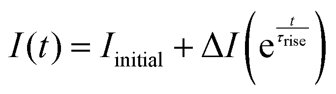
| Fig. 5 (a) ON–OFF measurements under visible light at 32.85 mW cm−2, showing the highest current increase for blue light (455 nm) and progressively lower increases for green (530 nm), yellow (590 nm), and red (630 nm).(b) Plot of current change (ΔA) versus wavelength, highlighting maximum enhancement for blue light, decreasing for longer wavelengths. (c)–(f) Dynamic response analysis for each wavelength (455, 530, 590, 630 nm), with current rise and decay fitted using exponential growth and decay functions. Shorter wavelengths show faster rise times (τrise) and varied decay times (τdecay), indicating efficient carrier dynamics. | ||
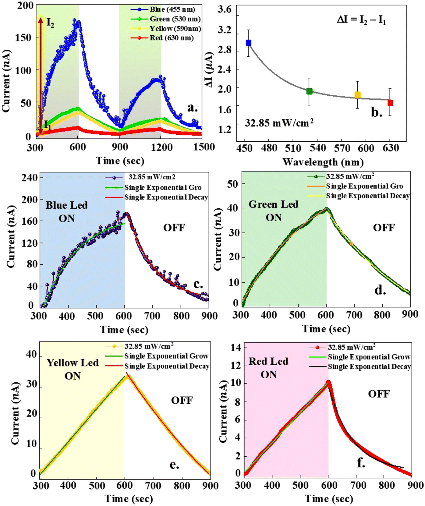
To quantify the change in current during illumination, we defined I1 as the initial current level in the dark and I2 as the current level after switching the light on. The change in current, (ΔI = I2 − I1), was calculated for each wavelength. The results are plotted as ΔI versus the wavelength of the LEDs, as shown in Fig. 5(b). This plot clearly illustrates the trend of current enhancement, with the maximum ΔI observed under blue light and progressively lower values for green, yellow, and red light. To understand the device's dynamic response to visible light, we selected one ON–OFF cycle from each set of measurements. The rise in current when light is ON and the decay in current when light is OFF is analyzed.
The rise in current during the light ON phase was modeled using the single exponential growth function:
 | (1) |
 represents the exponential increase of the current over time. The values for τrise are 124.6 s (blue), 264.6 s (green), 2846.8 s (yellow), and 993.5 s (red), showing the fastest response to blue light. A smaller τrise indicates a faster response to light. The rise in current was more pronounced for shorter wavelengths like blue (455 nm) and then green (530 nm) due to the higher photon energy and greater carrier generation. Similarly, the decay in current during the light OFF phase was modeled using the single exponential decay function:
 | (2) |
 ensures that the current follows an exponential decay over time. A smaller τdecay means a faster recombination process, whereas a larger τdecay indicates a slower decay due to carrier trapping. The decay times (τdecay), representing carrier recombination or trapping, varied across wavelengths, influenced by the energy of the incident photons and the density of trap states within the device. τdecay for blue, green, yellow and red are 96.01 s, 313.86 s, 678.78 s, and 86.11 s respectively. Analyzing the time constants reveals wavelength-dependent response trends, highlighting the device's potential for dynamic photodetection and wavelength-specific light sensing. The long τrise observed under yellow light illumination (2846.8 s) is attributed to the combined effect of slow charge transport in the CQDs–indigo matrix and the presence of deep trap states. These traps capture photogenerated carriers and gradually release them over time, thereby delaying the steady-state current.
Photodetection performance of the fabricated device is calculated in terms of responsivity (R) and detectivity (D*) as follows:
 | (3) |
 | (4) |
| Material | Exc. wavelength (nm) | (PPC, NPC) modulator | Responsivity (mA W−1) | Detectivity (Jones) | ON/OFF ratio | Ref. |
|---|---|---|---|---|---|---|
| MoS2/graphene/Ge | 532, 1550 | λ | 8000, 1100 | 1 × 10¹¹, 1 × 10⁷ | — | 50 |
| In2O3/Al2O3/Y6 | 365, 808 | λ | 100, 380 | — | — | 51 |
| CsPbI3-ITO-NHJs | 405 | V DS | 3.3, 335 | 6.8 × 10⁹, 6.7 × 10¹⁰ | 2.5, 1.8 | 52 |
| CsPbBr3-ITO-NHJs | 405 | V DS | 6.1, 186 | 1.6 × 10¹⁰, 4.9 × 10¹⁰ | 2, 1.9 | 52 |
| MoS2/BP | 840, 690 | λ | 200, −800 | 9.3 × 10⁹, 5.6 × 10⁹ | 320, 100 | 29 |
| CsPbBr3 QDs (7 nm) | 365, 450 | λ | 146, 1046 | 1.54 × 10¹¹, 1.65 × 10¹¹ | 64.4, 281 | 40 |
| InSe, MLG/InSe | 365 | — | 6.97, 18.8 | 1.2 × 10¹⁰, 2.5 × 10¹⁰ | 50.0, 180 | 53 |
| NiO/NB-rGO | 375 | Bias voltage | 800 | 9.4 × 10¹¹ | 120 | 54 |
| Multilayer MoS2 | 454, 980 | λ | 1 × 10⁸, 2.3 × 10³ | — | 1.3, 1.01 | 55 |
| Graphene/InSe/h-BN | 405 | Laser power | 1.3 × 10⁴, 1.1 × 10⁴ | — | — | 56 |
| Bi2O2Se/graphene | 635, 365 | λ | 8.8 × 10⁴, 11 × 104 | — | — | 57 |
| 2D Cr2Ge2Te6 | 635 | Light intensity | 340 × 103 | — | — | 58 |
| CQDs + indigo | 275, 375 | λ (NPC) | 1947.66, 954.611 | 3.94 × 10¹⁴, 2.84 × 10¹⁴ | 5.82, 8.26 | This work |
| CQDs + indigo | 455 | λ (PPC) | 0.0053 | 4.17 × 10¹¹ | 35.22 | This work |
| CQDs + indigo | 530 | λ (PPC) | 0.012 | 3.76 × 10¹¹ | 120.33 | This work |
| CQDs + indigo | 590 | λ (PPC) | 0.0096 | 9.92 × 10¹⁰ | 11.74 | This work |
| CQDs + indigo | 630 | λ (PPC) | 0.0032 | 2.03 × 10¹¹ | 136.17 | This work |
4 Conclusion
This work establishes the bidirectional photoresponse of the Pt/CQDs + indigo/Pt device, with wavelength sensitivity contributed by both CQDs and indigo, and demonstrates its potential as a versatile and multifunctional platform for advanced optoelectronic applications. In the UV region, the device showcases a negative photoconductive (NPC) response, attributed to carrier trapping and recombination phenomena, which provides an additional functional dimension. The device exhibits positive photoconductivity (PPC) under visible light, showing small wavelength dependence, yet showing positive photoconductivity. Furthermore, its dynamic response, characterized by rapid rise and decay times, underscores the potential of the device for real-time dynamic signal processing. This dual response extends the operational bandwidth from visible to UV regions, making the device suitable for broadband photodetection. Notably, the unique combination of PPC under visible light and NPC under UV light enables novel applications in optical synaptic systems. Visible light can effectively create optical memory by leveraging the positive photoconductive response, while UV light exposure offers a reliable mechanism for memory erasure. These features highlight the device's potential for innovative neuromorphic computing architectures, optical memory storage, and wavelength-selective photodetection systems.Author contributions
A. B. M.: conceptualization, data curation, formal analysis, investigation, visualization, writing – original draft, writing – reviewing and editing; R. T.: conceptualization, methodology, project administration resources, supervision, validation, visualization, writing – original draft, writing – reviewing and editing.Conflicts of interest
There are no conflicts to declare.Data availability
The relevant data has been uploaded to https://doi.org/10.7910/DVN/PNKPEA.Acknowledgements
A. B. M. would like to thank the Centre for Functional Materials (CFM), Vellore Institute of Technology for their support during this research work. R. T. acknowledges the Centre for Functional Materials for infrastructure and also to the Core Research Grant (CRG/2022/005093) from the Science and Engineering Board (SERB), India.References
- F. Gao and E. Reichmanis, Chem. Rev., 2023, 123, 10835–10837 CrossRef CAS PubMed.
- W. Rehm, R. Fischer, J. Stuke and H. Wagner, Phys. Status Solidi B, 1977, 79, 539–547 CrossRef CAS.
- M. Sun, Q. Fang, Z. Zhang, D. Xie, Y. Sun, J. Xu, W. Li, T. Ren and Y. F. Zhang, ACS Appl. Mater. Interfaces, 2018, 10, 7231 CrossRef CAS PubMed.
- J. Euvrard, S. Pournia, O. Gunawan and D. B. Mitzi, Appl. Phys. Lett., 2025, 126, 063302 CrossRef CAS.
- Q. Qiu and Z. Huang, Adv. Mater., 2021, 33, 2008126 CrossRef CAS PubMed.
- Y. Sun, Y. Ding and D. Xie, Adv. Funct. Mater., 2021, 31, 2105625 CrossRef CAS.
- M. C. Gupta, J. T. Harrison and M. T. Islam, Mater. Adv., 2021, 2, 3133–3160 RSC.
- Z. Zhao, J. Liu, Y. Liu and N. Zhu, J. Semicond., 2017, 38, 121001 CrossRef.
- X. Dong, X. Chen, X. Jiang and N. Yang, Adv. Energy Mater., 2023, 13(38), 2301143 CrossRef CAS.
- A. Grillo, E. Faella, A. Pelella, F. Giubileo, L. Ansari, F. Gity, P. K. Hurley, N. McEvoy and A. Di Bartolomeo, Adv. Funct. Mater., 2021, 31, 2105722 CrossRef CAS.
- S. Ratha, A. J. Simbeck, D. J. Late, S. K. Nayak and C. S. Rout, Appl. Phys. Lett., 2014, 105, 243502 CrossRef.
- B. Lee, X. Zhang, J. Kang, B. J. Jeong, S. Cho, K. H. Choi, J. Jeon, S. H. Lee, D. Kim, Y. H. Kim, J.-H. Kim, H. K. Yu and J.-Y. Choi, Nanoscale, 2024, 16, 20312–20318 RSC.
- B. Sreelakshmi and R. Thamankar, Mater. Adv., 2024, 5, 5912–5921 RSC.
- Y. Lv, F. Chen, Z. Zhang, J. Chen, X. Tang, Z. Shi, Q. Cui and C. Xu, Appl. Phys. Lett., 2022, 121, 061902 CrossRef CAS.
- S. C. Singh, Y. Peng, J. Rutledge and C. Guo, ACS Appl. Electron. Mater., 2019, 1, 1169–1178 CrossRef CAS PubMed.
- W. Ruan and X. Meng, ACS Appl. Nano Mater., 2023, 6, 1019–1026 CrossRef CAS.
- N. Tailor, C. Aranda, M. Saliba and S. Satapathi, ACS Mater. Lett., 2022, 4, 2298–2320 CrossRef CAS.
- C. Biswas, F. Güneş, D. D. Loc, S. C. Lim, M. S. Jeong, D. Pribat and Y. H. Lee, Nano Lett., 2011, 11, 4682–4687 CrossRef CAS PubMed.
- P.-F. Wang, Y. Liu, J. Yin, W. Ma, Z. Dong, W. Zhang, J.-L. Zhu and J.-L. Sun, J. Mater. Chem. C, 2019, 7, 887–896 RSC.
- A. Kumar, K. Intonti, L. Viscardi, O. Durante, A. Pelella, O. Kharsah, S. Sleziona, F. Giubileo, N. Martucciello, P. Ciambelli, M. Schleberger and A. Di Bartolomeo, Mater. Horiz., 2024, 11, 2397–2405 RSC.
- L. Hu, J. Yang, J. Wang, P. Cheng, L. O. Chua and F. Zhuge, Adv. Funct. Mater., 2021, 31, 2005582 CrossRef CAS.
- S. Ma, G. Li, Z. Li, T. Wang, Y. Zhang, N. Li, H. Chen, N. Zhang, W. Liu and Y. Huang, Adv. Mater., 2024, 36, 2305709 CrossRef CAS PubMed.
- A. Vardi, G. Bahir, S. E. Schacham, P. K. Kandaswamy and E. Monroy, J. Appl. Phys., 2010, 108, 104512 CrossRef.
- S. Kaushik, A. K. Kapoor, R. K. Pant, S. B. Krupanidhi and R. Singh, Opt. Mater., 2021, 121, 111553 CrossRef CAS.
- Y. Han, X. Zheng, M. Fu, D. Pan, X. Li, Y. Guo, J. Zhao and Q. Chen, Phys. Chem. Chem. Phys., 2016, 18, 818–826 RSC.
- M. A. Haque, J.-L. Li, A. L. Abdelhady, M. I. Saidaminov, D. Baran, O. M. Bakr, S.-H. Wei and T. Wu, Adv. Opt. Mater., 2019, 7, 1900865 CrossRef CAS.
- N. K. Tailor, P. Maity, M. I. Saidaminov, N. Pradhan and S. Satapathi, J. Phys. Chem. Lett., 2021, 12, 2286–2292 CrossRef CAS PubMed.
- H. Zhang, H. Li, F. Wang, X. Song, Z. Xu, D. Wei, J. Zhang, Z. Dai, Y. Ren, Y. Ye, X. Ren and J. Yao, ACS Appl. Electron. Mater., 2022, 4, 5177–5183 CrossRef CAS.
- H. Jawa, A. Varghese, S. Ghosh, S. Sahoo, Y. Yin, N. V. Medhekar and S. Lodha, Adv. Funct. Mater., 2022, 32, 2112696 CrossRef CAS.
- D. H. Kim, W. Lee and J.-M. Myoung, Nanoscale, 2018, 10, 17705–17711 RSC.
- J. Shen, W. Zhu, Z. Lian, A. Lin, S.-F. Shi, K. Yang, M. Li, D. Zhao, Y.-Y. Sun and J. Lian, ACS Appl. Electron. Mater., 2023, 5, 5291–5302 CrossRef CAS.
- W. Chen, L. Shen, J. Chen, X. Zhu, X. Liu and Q. Li, Optik, 2023, 287, 171133 CrossRef CAS.
- Y. Sun, L. Jiang, Z. Wang, Z. Hou, L. Dai, Y. Wang, J. Zhao, Y.-H. Xie, L. Zhao, Z. Jiang, W. Ren and G. Niu, ACS Nano, 2022, 16, 20272–20280 CrossRef CAS PubMed.
- M. Engel, M. Steiner and P. Avouris, Nano Lett., 2014, 14, 6414–6417 CrossRef CAS PubMed.
- A. M. Scheuermann, H. Wakidi, A. T. Lill, S. Oh, L. C. Llanes, C. A. D’Ambra, S. Antoine, M. Wang, M. L. Chabinyc, T.-Q. Nguyen, J. Read de Alaniz and C. M. Bates, ACS Appl. Polym. Mater., 2021, 3, 5125–5133 CrossRef CAS.
- A. A. Ahmed, M. Hashim, T. F. Qahtan and M. Rashid, Optik, 2022, 255, 168694 CrossRef CAS.
- S. Bansal, K. Prakash, K. Sharma, N. Sardana, S. Kumar, N. Gupta and A. K. Singh, Nanotechnology, 2020, 31, 405205 CrossRef CAS PubMed.
- S. Bansal, S. Kumar, A. Jain, V. Rohilla, K. Prakash, A. Gupta, T. Ali, A. M. Alenezi, M. S. Islam, M. S. Soliman and M. T. Islam, Sci. Rep., 2025, 15, 7762 CrossRef CAS PubMed.
- S. Bansal, A. K. Rajpoot, G. Chamundeswari, K. Prakash, P. R. Kumar, A. N. Z. Rashed, M. S. Soliman and M. T. Islam, J. Sci.: Adv. Mater. Devices, 2024, 9, 100798 CAS.
- J. An, G. Chen, X. Zhu, X. Lv, J. Bao and X. Xu, ACS Appl. Electron. Mater., 2022, 4, 1525–1532 CrossRef CAS.
- S. Ge, F. Huang, J. He, Z. Xu, Z. Sun, X. Han, C. Wang, L.-B. Huang and C. Pan, Adv. Opt. Mater., 2022, 10, 2200409 CrossRef CAS.
- Y. Jeong, T. Kim, H. Cho, J. Ahn, S. Hong, D. K. Hwang and S. Im, Adv. Mater., 2023, 35, 2304599 CrossRef CAS PubMed.
- D. Xue, W. Gong, C. Yan, Y. Zhang, J. Lu, Y. Yin, J. Zhang, Z. Wang, L. Huang and L. Chi, Adv. Funct. Mater., 2024, 34, 2402884 CrossRef CAS.
- A. B. Mishra and R. Thamankar, APL Mater., 2023, 11, 041122 CrossRef CAS.
- Y. Du, H. Pan, S. Wang, T. Wu, Y. P. Feng, J. Pan and A. T. S. Wee, ACS Nano, 2012, 6, 2517–2523 CrossRef CAS PubMed.
- G. Zhou, S. Duan, P. Li, B. Sun, B. Wu, Y. Yao, X. Yang, J. Han, J. Wu, G. Wang, L. Liao, C. Lin, W. Hu, C. Xu, D. Liu, T. Chen, L. Chen, A. Zhou and Q. Song, Adv. Electron. Mater., 2018, 4, 1700567 CrossRef.
- H.-L. Yang, L.-F. Bai, Z.-R. Geng, H. Chen, L.-T. Xu, Y.-C. Xie, D.-J. Wang, H.-W. Gu and X.-M. Wang, Mater. Today Adv., 2023, 18, 100376 CrossRef CAS.
- H. Ding, X.-H. Li, X.-B. Chen, J.-S. Wei, X.-B. Li and H.-M. Xiong, J. Appl. Phys., 2020, 127, 231101 CrossRef CAS.
- S. E. Elugoke, G. E. Uwaya, T. W. Quadri and E. E. Ebenso, Carbon Quantum Dots: Basics, Properties, and Fundamentals, 2024, ch. 1, pp. 3–42 Search PubMed.
- J. You, Z. Han, N. Zhang, Q. Zhang, Y. Zhang, Y. Liu, Y. Li, J. Ao, Z. Jiang, Z. Zhong, H. Guo, H. Hu, L. Wang and Z. Zhu, Adv. Sci., 2024, 11, 2404336 CrossRef CAS PubMed.
- D. Li, H. Ren, Y. Chen, Y. Tang, K. Liang, Y. Wang, F. Li, G. Liu, L. Meng and B. Zhu, Adv. Funct. Mater., 2023, 33, 2303198 CrossRef CAS.
- Q. He, G. Chen, Y. Wang, X. Liu, D. Xu, X. Xu, Y. Liu, J. Bao and X. Wang, Small, 2021, 17, 2101403 CrossRef CAS PubMed.
- B. Cui, Y. Xing, K. Niu, J. Han, H. Ma, W. Lv, T. Lei, B. Wang and Z. Zeng, J. Sci.: Adv. Mater. Devices, 2022, 7, 100484 CAS.
- C. Walleni, N. Hamdaoui, S. B. Malik, M. F. Nsib and E. Llobet, J. Alloys Compd., 2024, 976, 173248 CrossRef CAS.
- J.-Y. Wu, Y. T. Chun, S. Li, T. Zhang, J. Wang, P. K. Shrestha and D. Chu, Adv. Mater., 2018, 30, 1705880 CrossRef PubMed.
- Z. Gao, R. Jiang, M. Deng, C. Zhao, Z. Hong, L. Shang, Y. Li, L. Zhu, J. Zhang, J. Zhang and Z. Hu, Adv. Mater., 2024, 36, 2401585 CrossRef CAS PubMed.
- C.-M. Yang, T.-C. Chen, D. Verma, L.-J. Li, B. Liu, W.-H. Chang and C.-S. Lai, Adv. Funct. Mater., 2020, 30, 2001598 CrossRef CAS.
- L. Xie, L. Guo, W. Yu, T. Kang, R.-K. Zheng and K. Zhang, Nanotechnology, 2018, 29, 464002 CrossRef PubMed.
Footnote |
| † Electronic supplementary information (ESI) available. See DOI: https://doi.org/10.1039/d5ma00439j |
| This journal is © The Royal Society of Chemistry 2025 |