
 Open Access Article
 This Open Access Article is licensed under a Creative Commons Attribution-Non Commercial 3.0 Unported Licence
A DFT insight into lead free double halide perovskite Cs2TeI6 for clean and renewable energy sources
Md. Sajib
Hossian
a,
Md. Majibul Haque
Babu
b,
Alamgir
Kabir
 *a,
Ahmed
Azzouz Rached
c and
Md. Ibrahim
Kholil
d
*a,
Ahmed
Azzouz Rached
c and
Md. Ibrahim
Kholil
d
aDepartment of Physics, University of Dhaka, Dhaka-1000, Bangladesh. E-mail: alamgir.kabir@du.ac.bd
bBasic Science Division, World University of Bangladesh, Dhaka-1205, Bangladesh
cFaculty of Sciences, Saad Dahleb University of Blida 1, Route de Soumaa, B.P. 270, Blida, Algeria
dDepartment of Physics, Pabna University of Engineering and Technology, Pabna, Bangladesh
First published on 16th June 2025
Abstract
In this study, we investigate the lead free double halide perovskite Cs2TeI6 using first-principles density functional theory (DFT) calculations to explore its potential as a photocatalyst for water splitting. We employ multiple exchange–correlation functionals to comprehensively evaluate the material's mechanical, electronic, and optical properties. The elastic constants, bulk modulus, and hardness indicate that Cs2TeI6 is mechanically stable and ductile, with a Vickers hardness value between 0.13–2.28 GPa. The band structure analysis reveals an indirect bandgap ranging from 1.268 to 2.058 eV, depending on the functional used. Optical property simulations demonstrate significant absorption in the visible range, with the calculated redox potentials suggesting thermodynamically favorable conditions for the water splitting mechanism. The findings indicate that Cs2TeI6 is a promising candidate for photocatalytic applications, including solar energy conversion and hydrogen production.
1. Introduction
Photocatalytic water splitting has emerged as a pivotal technology for sustainable hydrogen production, addressing the need for clean and renewable energy sources. By harnessing solar energy to convert water into hydrogen and oxygen, this process offers a viable solution to reduce dependence on fossil fuels and mitigate environmental impacts.1,2 The ideal photocatalyst must possess a suitable band gap (typically between 1.23 and 3.00 eV) for optimal light absorption, and favorable redox potentials for the hydrogen and oxygen evolution reactions.3,4 In the cutting-edge world, perovskites are rare minerals found on earth with a cubic structure that have gained significant attention as potential candidates in optoelectronics. Among them, the semiconducting lead halide perovskites, i.e. ABX3, have a broad range of optoelectronic device applications such as photovoltaics, solar cells, light-emitting diodes (LEDs), optical fibres,5–9etc. Primarily, the lead-based halide perovskite was used as an optical material in solar cells with low power conversion efficiency (PCE), around 3.8%.10 In the years that followed, the efficiency of lead-based perovskite solar cells was enhanced, and they became the subject of a significant amount of study worldwide. Recently the PCE of perovskite solar cells has reached a new high of 25.2%.11–16Despite so many advantages, the prime disadvantages of lead-based halide perovskites are their toxicity and instability under ambient conditions. Therefore, scientists all over the world are working to develop lead-free perovskite materials which are less toxic and more stable in the ambient environment. The divalent non-toxic metals in group IV(A), i.e., Sn and Ge, were considered suitable alternatives for lead retaining the ABO3 structure. However, due to the 2+ oxidation state, the Sn-based perovskite rapidly degrades when exposed to the air.17 Moreover, Ge-based perovskites showed poor photovoltaic performance.18 Meanwhile, the substitution of other divalent elements revealed poor optoelectronic performance due to low absorption, large carrier effective mass, and high bandgap.19,20 Recently, it was postulated that two Pb2+ ions might be exchanged by the combination of one monovalent and one metallic trivalent ion, or by the combination of one monovalent and one tetravalent metal to produce perovskites that have the same overall charge balance. As a result of this unique substitution, double perovskites with general formula A2B′B′′X6 can be synthesized easily. The A site in the formula is usually occupied by a moderately large cation, the B′ and B′′ sites are occupied by either trivalent or monovalent cations, and the X site is an halogen or oxygen ion. Given their potential to solve the problems that have plagued lead-based perovskites thus far, halide double perovskites have recently been a hot topic in the field of optoelectronics research.21 Recently, some studies have reported the synthesis process of several inorganic halide double perovskites, as well as their characterization. However, the majority of synthetic materials have either poor optical characteristics or high bandgap values; therefore, the materials are not suitable for photovoltaic applications. Eric et al. have reported bandgaps for Cs2AgBiBr6 as 2.19 eV and Cs2AgBiCl6 as 2.77 eV, and both materials are stable under exposure to the air; however, Cs2AgBiBr6 is found to degrade over time.22 Zhou et al. have reported the bandgap for Cs2AgInCl6 as 3.33 eV with excellent thermal stability.23 However, they suggested further investigations to improve the optical properties. Jani et al. have reported a PCE of 14.68% for Cs2TiBr6 that can be improved to 18.97% by compositional changes.24 Moreover, other halide double perovskites, for example, Cs2SnCl6, Cs2PdBr6 and Cs2PdX6 (X = Br, I), have demonstrated impressive optical performance and stability when subjected to the ambient environment.25–27 Recently, a relatively new halide double perovskite composition, Cs2TeI6, has shown impressive properties for use in optoelectronics applications.28 To our best knowledge, there is no extensive study on the technologically important mechanical properties of Cs2TeI6. Among lead-free alternatives, Cs2TeI6 distinguishes itself through its balanced optoelectronic properties. While Cs2AgBiBr6 exhibits a wider bandgap (∼2.2 eV) and stability issues under prolonged illumination,22 and Cs2TiBr6 shows stronger absorption but higher bandgap (∼1.8 eV),24 Cs2TeI6 achieves an optimal indirect bandgap (∼1.5 eV) with enhanced visible-light absorption.28 Notably, its iodine composition improves environmental stability compared to bromine-based analogs (e.g., Cs2SnBr6 degrades within hours in air),29 while maintaining competitive power conversion efficiency potential (∼15–19%).30 These attributes make Cs2TeI6 a uniquely viable candidate for stable, visible-light-driven applications.
This study employs first-principles density functional theory (DFT) calculations to systematically investigate the structural, mechanical, electronic, and optical properties of Cs2TeI6. Our primary objectives are to evaluate its mechanical stability and ductility for potential use in thin-film technologies, determine its electronic band structure and bandgap to assess its suitability for visible-light absorption, analyze its optical properties to gauge its efficiency in solar energy conversion, and examine its redox potentials to determine its feasibility for photocatalytic water splitting. Through this comprehensive analysis, we aim to establish Cs2TeI6 as a viable, environmentally friendly material for clean energy applications, particularly in photocatalysis and photovoltaics.
2. Computational details
The full-potential linearized augmented plane wave method31,32 based on DFT,33 as available in the WIEN2k package,34 is used for all the calculations. In order to improve the results of the electronic properties, the GGA-mBJ method was used in the calculations.35 The maximum allowable value of the Gmax parameter, which is the highest vector magnitude in a Fourier expansion, is set to 14. The cut-off energy, which was set at −6 Ry, was chosen so that valence states could be distinguished from core states. The charge convergence of 0.0001e is used within a self-consistency cycle. For the Brillouin zone sampling, a special k-point mesh of 8 × 8 × 8 in the Monkhorst–Pack scheme is used. K-Point convergence tests were performed and revealed very small energy variations (0.0002 Ry) between 8 × 8 × 8 and 12 × 12 × 12 meshes for both PBE and GGA-PBEsol. The cut-off energy convergence was set at −6 Ry by checking its very small variation (≤0.000006) Ry between −5 Ry and −8 Ry. The elastic constants were calculated using the finite-strain energy method within the WIEN2k code,36 where a series of small deformations were applied to the equilibrium lattice, and the resulting energy-strain curves were fitted to determine the elastic tensor. Atomic positions were fully relaxed for each strain state to ensure equilibrium conditions. The methodology follows the approach implemented in the Elastic package37 and aligns with previous first-principles studies on similar systems.38,39 The elastic constants were calculated using the finite-strain energy method40 within the WIEN2k code,34 where a series of small deformations were applied to the equilibrium lattice, and the resulting energy-strain curves were fitted to determine the elastic tensor. Atomic positions were fully relaxed for each strain state to ensure equilibrium conditions. The mechanical properties were calculated using the CASTEP code.41 The residual force 0.03 eV Å−1 was included as a supreme value. Optical properties were derived from the dielectric tensor , covering photon energies up to 14 eV.
3. Results and discussion
3.1. Structural properties
The ternary halide double perovskite Cs2TeI6 possesses a face-centred cubic crystal with space group Fm![[3 with combining macron]](https://www.rsc.org/images/entities/char_0033_0304.gif) m (no. 225).42 The crystal geometry of Cs2TeI6 is illustrated in Fig. 1, which can be expressed by the A2BX6 formula. This can be defined as a [BX6] cluster with B-deficient ABX3 perovskites. In addition, vacant or unfilled sites between two [BX6] are occupied with A-site atoms. Each [BX6] unit in the A2BX6 structure is isolated from others, establishing a 12-fold coordination environment of discrete X-anions. Moreover, A(Cs)-cations are encircled by twelve and B(Te) atoms by six halogen ions. The A-site atoms are placed at the 8c Wyckoff site with (0.25, 0.25, 0.25) fractional coordinates, B-site cations are positioned at the 4a Wyckoff site with (0, 0, 0) coordinates, and finally, X-anions lie at the 24e Wyckoff site with (0.2498, 0, 0) fractional coordinates.
m (no. 225).42 The crystal geometry of Cs2TeI6 is illustrated in Fig. 1, which can be expressed by the A2BX6 formula. This can be defined as a [BX6] cluster with B-deficient ABX3 perovskites. In addition, vacant or unfilled sites between two [BX6] are occupied with A-site atoms. Each [BX6] unit in the A2BX6 structure is isolated from others, establishing a 12-fold coordination environment of discrete X-anions. Moreover, A(Cs)-cations are encircled by twelve and B(Te) atoms by six halogen ions. The A-site atoms are placed at the 8c Wyckoff site with (0.25, 0.25, 0.25) fractional coordinates, B-site cations are positioned at the 4a Wyckoff site with (0, 0, 0) coordinates, and finally, X-anions lie at the 24e Wyckoff site with (0.2498, 0, 0) fractional coordinates.
 | ||
| Fig. 1 (a) Reorientation of the unit cell reveals the isolated polyhedral units and (b) crystal structure of the double perovskite. | ||
However, we have simulated the lattice parameters under two different methods, which are GGA-PBE and GGA-PBEsol functions. Table 1 illustrates the simulated lattice parameters in comparison to the experimental results. The lattice constants are determined to be quite close to the experimental value. Exploring Table 1, it is obvious that the GGA-PBEsol method gives more precise lattice parameter values compared with practical work than the GGA-PBE method.
3.2. Mechanical properties
To project the stability of the Cs2TeI6 double perovskite, three related elastic constants for a cubic crystal, namely C11, C12, and C44, have been investigated precisely using the finite strain theory40 within the CASTEP code. In general, the calculated elastic constants should satisfy the following Born stability requirement to be mechanically stable.43 Thus, for a cubic phase, the Born stability criteria are specified as follows:| C11 + 2C12 > 0, C44 > 0, C11 − C44 > 0 |
Subsequently, the values of the three corresponding elastic constants are listed in Table 2 for both the PBE and PBEsol functional. The Cs2TeI6 satisfies the above-Born stability criteria, i.e. three single elastic constants fulfil these criteria, demonstrating that it is mechanically stable. It is ubiquitously known that Cauchy pressure typically demonstrates the difference between C12 and C44, and its positive and negative value indicates the ductile and brittle nature. Herein, we found only a negative value of Cauchy pressure, signifying the brittle nature of Cs2TeI6.
| Functional | C 11 | C 12 | C 44 | C 12 − C44 |
|---|---|---|---|---|
| PBE | 23.68 | 2.67 | 6.94 | −4.27 |
| PBEsol | 42.59 | 7.79 | 10.07 | −2.28 |
However, using the Voigt–Reuss–Hill (VRH) equating methodology, the polycrystalline elastic moduli of Cs2TeI6, and the Poisson's ratio, have been computed.44 Any cubic crystal's Voigt and Reuss constraints on B and G have been determined using these formulas:44
 | (1) |
 | (2) |
 | (3) |
The arithmetic mean (AM) value of Voigt and Reuss in terms of Hill approximation was determined as follows:
 | (4) |
 | (5) |
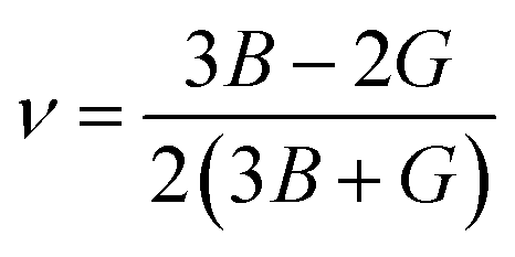
The use of Hill's bulk modulus (B) and shear modulus (G) yields Young's modulus (E) and Poisson's ratio (ν), respectively:
 | (6) |
 | (7) |
The calculated bulk and shear modulus mainly measure the elasticity in size and elasticity in shape, respectively. Additionally, shear modulus indicates the plastic deformation under shear stress and hence suggests the materials hardness.45 The calculated results of polycrystalline elastic modulus are recorded in Table 3. It is manifested (see Table 3) that B is considerably larger than G, i.e. B > G, which designates that G is desirable to describe the stability of Cs2TeI6.46 Besides, a lower value of G than B reflects a higher resistance to the volume deformation under external pressure and reveals a covalent nature in the atomic bonds.47 Most importantly, the B and G values are relatively lower in the case of the PBE and PBEsol methods as they are less than 100 GPa,48 revealing a soft and flexible nature. Therefore, Cs2TeI6 is suitable to use in thin film technology and remarkable for use in optoelectronic device applications.
| Functional | B (GPa) | G (GPa) | β (1/GPa) | μ M | E (GPa) | B/G | ν | H v (GPa) |
|---|---|---|---|---|---|---|---|---|
| PBE | 9.67 | 5.86 | 0.1034 | 1.39 | 14.63 | 1.65 | 0.247 | 0.13 |
| PBEsol | 19.39 | 12.55 | 0.0515 | 1.93 | 30.97 | 1.55 | 0.234 | 2.28 |
It is seen from Table 3 that a lower value of compressibility, i.e.β (= 1/B), is obtained for the PBE and PBEsol functionals as they are inversely proportional to the bulk modulus. Conversely, a higher value of machinability index (μM = B/C44) is determined for Cs2TeI6 double perovskite, which is similar to previously reported data.49 Therefore, we can conclude that Cs2TeI6 may have a plausible application in materials engineering.49 It can also be seen (see Table 4) that E discloses a higher value than G and B, i.e. the moduli enhance in the order of G < B < E, which signifies that Cs2TeI6 double perovskite allows uniaxial deformation more easily than volumetric deformation. Moreover, it should be noted that a lower value E is confirmed by the PBE and PBEsol methods, signifying a soft and flexible material, which is optimum for making a high-quality thin film.
| Compounds | Functionals | Nature | Band gap, Eg (eV) | Ref. |
|---|---|---|---|---|
| Cs2TeI6 | PBE | Indirect | 1.268 | This work |
| PBE_mBJ | Indirect | 1.718 | This work | |
| PBEsol | Indirect | 1.287 | This work | |
| PBEsol_mBJ | Indirect | 1.706 | This work | |
| — | Indirect | 1.50 | Expt.28 | |
| PBE | Indirect | 1.12 | Calc.30 | |
| Cs2PtI6 | PBE | Indirect | 0.651 | 50 |
| Rb2TeBr6 | — | Indirect | 2.07 | 51 |
| Rb2SnI6 | PBE | Indirect | 0.12 | 50 |
| K2TeBr6 | — | Indirect | 2.39 | 51 |
To explore the brittleness and ductility of Cs2TeI6 further, we computed the Poisson's ratios and Pugh's.52,53 In general, the value of ratio B/G = 1.75 determines the ductile and brittle nature of the materials. Herein, the material can be considered brittle as the value of B/G is lower than 1.75 with the PBE and PBEsol functionals. In the case of Poisson's ratio, Cs2TeI6 double perovskite exhibits a brittle nature as the Poisson's ratio is less than the critical value of 0.26 in both functions. Both Pugh's ratio and Poisson's ratio indicate the brittleness of the materials and the same results indicate the reliability of our calculations.
The structural and elastic properties of Cs2TeI6 are intrinsically linked due to its face-centered cubic (FCC) symmetry and unique bonding environment. The material's large lattice parameter (*a* ≈ 11.70–11.96 Å) and isolated [TeI6]2− octahedra result in low bulk modulus (B = 9.67–19.39 GPa) and shear modulus (G = 5.86–12.55 GPa), characteristic of soft, brittle materials.28,29 The negative Cauchy pressure (C12 − C44 = −4.27 to −2.28 GPa) and low B/G ratio (1.55–1.65) further confirm this brittle behavior, consistent with other vacancy-ordered double perovskites.29,49 Notably, the PBEsol functional predicts shorter bond lengths and higher bond overlap population values compared to PBE, correlating with increased covalency and greater hardness (2.28 GPa vs. 0.13 GPa).49,54 These structure–property relationships highlight how computational methods influence mechanical predictions while underscoring Cs2TeI6's potential for flexible optoelectronic applications.28,48
The Vickers hardness Hv, is calculated here by using the following empirical formula,55 where k = G/B.
| Hv = 2(k2G)0.585 − 3 | (8) |
The calculated value of Vickers hardness, such as 0.13 GPa and 2.28 GPa for the PBE and PBEsol functional, respectively, indicates that each value is small and hence it reveals the soft and flexible nature of the material, and hence it is suitable to be used in thin films. The Vickers hardness of Cs2TeI6 (0.13–2.28 GPa) is notably low compared to other functional materials but aligns with trends observed in halide perovskites. For instance, lead-free double perovskites like Cs2SnI6 and Cs2AgBiBr6 exhibit similarly low hardness (0.5–1.5 GPa) due to their ionic bonding and structural vacancies.22,28 In contrast, hybrid perovskites (e.g., MAPbI3) show marginally higher values (∼0.3–1.0 GPa) owing to partial covalent contributions from organic cations,56 while oxide perovskites (e.g., SrTiO3) are significantly harder (10–20 GPa) because of stronger metal–oxygen bonds.45 Conventional semiconductors like silicon (∼10 GPa) and GaAs (∼7 GPa) also far exceed Cs2TeI6 in hardness,55,57 highlighting the soft nature of halide perovskites. These comparisons underscore that Cs2TeI6's low hardness is intrinsic to its chemical class, making it suitable for flexible optoelectronics but mechanically inferior to oxides or covalent semiconductors.
3.3. Electronic properties
Electronic properties are very crucial properties for getting fruitful information from double perovskites. We studied the electronic properties utilizing GGA along with PBE and GGA along with PBEsol in the Brillouin zones. For better estimation, we did further simulation using the GGA-PBE functional along with mBJ and also added mBJ with GGA-PBEsol. Here, four different band gaps are found from those calculations. In this simulation, we calculated the band near the Fermi level as the semi-conductive theory enforces that the bands are very important for finding the physical behavior of the material. The valence band maximum (VBM) is observed at a different point from the conduction band minimum (CBM), which indicates that Cs2TeI6 is an indirect band gap semiconductor. For GGA, along with four different functionals of PBE, PBE-mBJ, PBEsol, and PBEsol-mBJ, our simulated indirect band gap values are 1.268 eV, 1.718 eV, 1.287 eV, and 1.706 eV, which are depicted in Fig. 2. In Fig. 2, the total density of states (TDOS) with the band structure for every type of function is also added. The experimental band gap of Cs2TeI6 is 1.5 eV,28 which is in the range of our simulated band gap. The calculated band gap with different functionals is recorded in Table 4. In every function, it is observed non-zero TDOS at the Fermi level, which clarified that our material is a semiconductor. The calculated bandgap of Cs2TeI6 shows strong dependence on the choice of exchange–correlation functional, varying from 1.268 eV (GGA-PBE) to 2.058 eV (PBEsol-mBJ), while the experimental value is reported as 1.5 eV.28,30 This wide range originates from the inherent limitations of different DFT functionals in describing electronic structure – GGA functionals like PBE tend to underestimate the bandgaps due to the self-interaction error, while mBJ corrections incorporate nonlocal potential effects that typically yield larger, more accurate gaps.35 The functional dependence is particularly pronounced in halide perovskites due to their strong spin–orbit coupling and localized electronic states. Notably, the PBEsol-mBJ result (1.706 eV) agrees most closely with experiments, suggesting that this approach may better capture the material's electronic properties.30 Such variations in predicted bandgap have direct consequences for assessing the material's suitability for specific applications, as they affect both optical absorption characteristics and the alignment of the band edges with the redox potentials.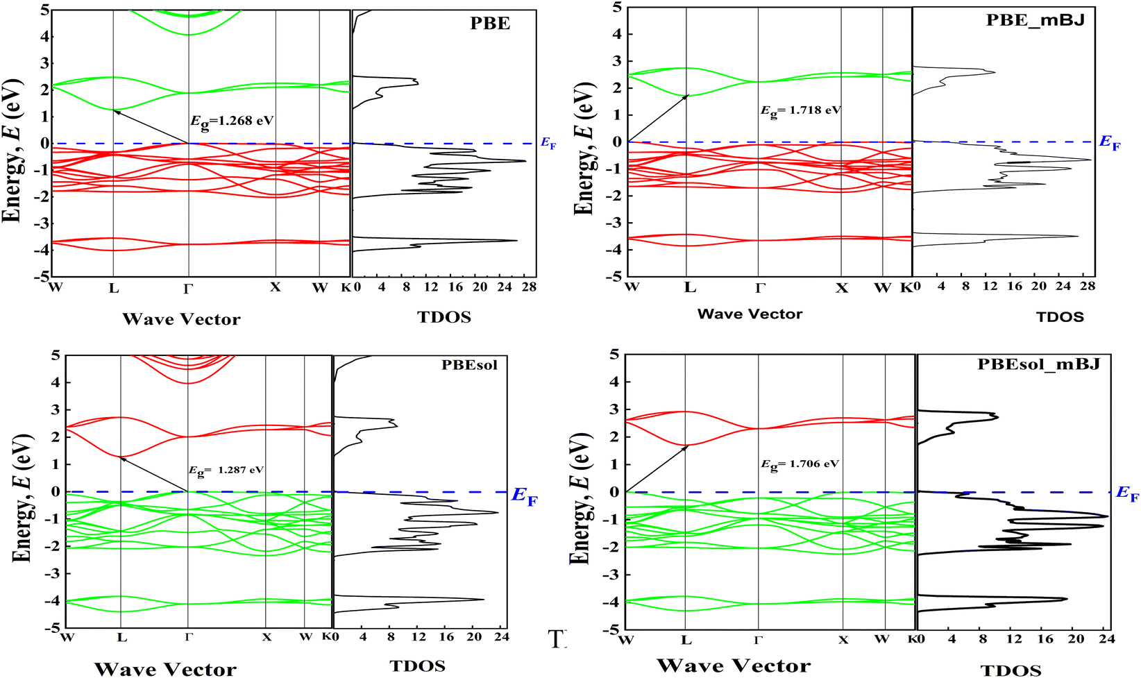 | ||
| Fig. 2 Calculated band structure along with TDOS under five different density functionals. | ||
3.4. Charge density and bond length
Fig. 3 represents the contour plot of the electronic charge density of Cs2TeI6 along the 111 and 011 planes. Electronic charge density is calculated here to reveal the bonding nature among the different atoms. A vertical colour line on the right side represents the scale of low (blue) to high (red) electron density. The covalent bonds and the ionic bonds mainly define the charge accumulation and balancing of charges between two constitutes atoms, respectively.54 The charge density map represents both types of bonds due to charge accumulation and balancing charge between Cs, Te, and I. Consequently, covalent and ionic bonds were observed among the different atoms. | ||
| Fig. 3 Charge density of Cs2TeI6 along (a) the 111 plane and (b) the 011 plane. | ||
The investigated bond overlap population (BOP) is listed in Table 5. The negative and positive values of BOP indicate the bonding and antibonding state.58 Furthermore, the large value of BOP signifies the strong covalent interaction between the two atoms. Therefore, the Cs–Cs and Te–Cs bonds reveal a significant covalent interaction. Under the PBEsol, the bond length decreases (as shown in Fig. 4), but on the other side, an enhanced BOP value has been observed. Hence, the covalency of Cs2TeI6 is increased in PBEsol.
| Functional | Mulliken bond overlap population | |||
|---|---|---|---|---|
| Bond | Bond number nμ | Bond length, dμ (Å) | Bond overlap population, pμ | |
| PBE | Te–I | 6 | 2.979 | −0.47 |
| I–I | 12 | 4.213 | −0.26 | |
| I–Cs | 12 | 4.280 | −0.26 | |
| Te–Cs | 2 | 5.241 | 0.35 | |
| I–I | 3 | 5.958 | −0.39 | |
| Cs–Cs | 1 | 6.052 | 0.37 | |
| PBEsol | Te–I | 6 | 2.956 | −1.46 |
| I–I | 12 | 4.056 | −0.35 | |
| I–Cs | 12 | 4.118 | −0.68 | |
| Te–Cs | 2 | 5.044 | 0.97 | |
| I–I | 3 | 5.736 | −1.31 | |
| Cs–Cs | 1 | 5.824 | 0.73 | |
 | ||
| Fig. 4 Calculated bond length of Cs2TeI6. | ||
3.5. Redox potentials
A narrow bandgap (∼2.0 eV), the low electron–hole (e−–h) recombination rate and suitable redox potentials (RP) are important for a good photocatalyst. The RP is typically calculated from the position of the VBM and CBM as compared to the water oxidation/reduction potential. Herein, the positions of the VBM and CBM are theoretically calculated using the following equations: | (9) |
| EVB = ECB + Eg | (10) |
 | ||
| Fig. 5 The position of the CBM and VBM of Cs2TeI6 with water redox potential at pH = 0 for four functions. | ||
In order to achieve water splitting as a whole, the CBM needs to have lower value than the reduction potential of H+ to H2, assuming 0 eV vs. NHE at pH 0, and the VBM needs to have larger value than the oxidation potential of H2O to O2. Both of these conditions must be met for the CBM (1.23 eV vs. NHE). Therefore, the minimum required photon energy of 1.23 eV is required to drive the reaction. In the case of the PBE function, the positive value of VBM potential (1.22 eV vs. NHE) signifies that O2/H2O is not plausible owing to the thermodynamic aspect, while the CBM potential value is −0.047 eV. On the other hand, the other four functionals (i.e. PBEsol, PBE-mBj, PBEsol-mBj) firmly confirm that reduction of H2 and evolution of O2 are feasible in the Cs2TeI6 perovskite material. Thus, we can say that the splitting of water by Cs2TeI6 perovskite is thermodynamically auspicious, and it can be anticipated to be an effective candidate in the field of photocatalysis.59
3.6. Optical properties
Herein, we have investigated the most essential optical parameters such as absorption coefficient, reflectivity, refractive index, and dielectric function to justify the excellence of Cs2TeI6 in solar cells and other optoelectronic applications. These parameters are calculated and discussed here up to 14 eV of photon energy to understand the optical behaviour in visible light and high photon energy radiation. In the present investigation, we have also considered different functionals for various optical parameters to show the material response in visible and other energy regions and find suitable behaviour for solar cell material and other optoelectronic applications. The absorption coefficient is basically characterized by the ability to detect light penetration in the materials when a certain wavelength of light is shone on the material surface, and the light penetrates into the material until it is totally consumed.60 It is fundamental to demonstrate absorption behaviour as well as solar energy communication capabilities.For solar energy conversation capability, absorptive behaviour behaves as a significant parameter. The absorption coefficient of Cs2TeI6 is represented in Fig. 6 as a function of photon energy and wavelength. It is manifest from Fig. 6(a) that the absorption peak of PBEsol shifted towards the lower photon energy region as compared to the other functional. The change in functional shows enhanced absorption and large peaks in the visible region. A few notched-type peaks between 6 to 10 eV are observed in the absorption in the ultraviolet region, which further indicates the large absorption.
 | ||
| Fig. 6 Calculated absorption coefficient of Cs2TeI6 as a function of (a) energy and (b) wavelength. | ||
However, the peak for PBEsol largely shifted towards the visible region. Here, we also consider absorption as a function of the wavelength of incident light to clearly understand the absorptive behaviours in visible light. Consequently, we observed from Fig. 6(b) that the overall contribution of the PBEsol functional reveals significant absorption compared to other functionals in the visible region. As a result, the enhanced absorption of Cs2TeI6 in the visible, as well as high-energy region, obviously represents the greater ability of light absorption under different functionals. Therefore, the double halide perovskite Cs2TeI6 exhibits greater absorption and is hence suitable for application in solar cells and other optoelectronic devices.
The dielectric function is essential for understanding of charge-carrier recombination rate and the static value at zero energy in the real part of the dielectric functions is mainly responsible in that case. The calculated dielectric function (real part) is represented in Fig. 7(a), and a separate graph in Fig. 7(b) reveals the static value, ε1(0). The large static value represents the lower charge-carrier recombination rate. As a result, it increases the efficiency of the material and hence increases the suitability to use it in optoelectronic applications. It is manifest from Fig. 7(b) that the PBEsol functional shows a large static value. Therefore, we conclude that the charge-recombination rate under the PBEsol functional reduced more than other functionals and this enhanced the efficiency of Cs2TeI6 significantly. On the other hand, a material with a large value of band gap shows a lower dielectric value.61 In the present calculation, the PBE and PBEsol functionals show lower band gap values (as shown in Fig. 2) and accordingly reveal the high dielectric value, which is crucial for optoelectronic performance. The calculated imaginary part of the dielectric function is recorded in Fig. 7(c). The imaginary part is related to electronic band structure and is responsible for signifying the absorption nature.62Fig. 7 reveals the large peaks in the visible region and hence increases the absorption in that region (as shown in Fig. 6).
 | ||
| Fig. 7 The calculated dielectric functions (real parts): (a) as a function of energy and (b) static values at 0 eV. Imaginary part of the (c) dielectric functions and (d) refractive index are also depicted. | ||
The calculated value of the refractive index by using different functionals is represented in Fig. 8(a), and the obtained results found a similar pattern to the real part of the dielectric function. The recorded static values of the refractive index, n(0) are 2.61, 2.35, 2.65, and 2.37 for the PBE, PBE-mBJ, PBEsol, and PBEsol-mBJ functionals, respectively. The state values of GaAs between 3.29 and 3.86,63,64 and 3.8865 for Si are considered suitable values to use in photovoltaic applications. In the present calculation, the static values for different functionals approximately agree with the potential static value. Therefore, we conclude that Cs2TeI6 reveals a suitable nature to use in photovoltaic applications. On the other hand, we have found that the present calculation follows the relation n(0)2 ≈ ε1(0), which indicates the reliability of this investigation.66
 | ||
| Fig. 8 The simulated optical parameters of the double perovskite as a function of photon energy (eV). (a) Refractive index and (b) reflectivity. | ||
Fig. 7(d) reveals the imaginary part of the refractive index, which is also known as the extinction coefficient, k(ω). It indicates the absorption of light.40 Consequently, the extinction coefficient follows the imaginary part of the dielectric function, ε2(ω) as it is responsible for the absorption coefficient. The extinction coefficient shows it's initially very low absorption and in the visible region peak values are starting, which denotes favourable absorption in the visible and ultraviolet region as well. The low absorption in the visible region is mainly responsible for the transparent nature.66 The investigated reflectivity spectra as a function of photon energy are shown in Fig. 8(b). Reflectivity mainly determines the ability of the material to reflect the incident light on the material surface. It is manifest from Fig. 8(b) that the reflectivity in the visible and UV regions reflects higher values than the IR region, but these values are not considered high enough, and hence the material shows high absorption (Fig. 6) in the visible and UV region. As a result, the high absorptive and low reflectance nature of Cs2TeI6 in the visible, as well as ultraviolet region denotes the promising candidate for optoelectronic applications. The static dielectric constant (ε1(0)) and refractive index (n(0)) of Cs2TeI6 (ε1(0) ≈ 4.5–6.5, n(0) ≈ 2.35–2.65) are comparable to other lead-free halide perovskites. For instance, Cs2AgBiBr6 exhibits similar values (ε1(0) ≈ 5.2, n(0) ≈ 2.4),22 while Cs2SnI6 shows slightly higher dielectric response (ε1(0) ≈ 7.1) due to its more covalent bonding character.29 The lower ε1(0) of Cs2TeI6 relative to Cs2SnI6 suggests weaker screening of charge carriers, which may influence the exciton binding energies and charge recombination rates. However, its optical constants remain competitive with other vacancy-ordered double perovskites like Cs2PdBr6 (n(0) ≈ 2.3),26 underscoring its potential for optoelectronic applications. These comparisons highlight the role of structural vacancies and halide composition in tuning the dielectric properties across this material class.
3.7. Conclusion
This study comprehensively investigated the lead-free double halide perovskite Cs2TeI6 using density functional theory (DFT) to evaluate its potential for clean and renewable energy applications, particularly photocatalytic water splitting. The mechanical properties confirmed the material's stability and ductility, supported by elastic constants, bulk modulus, and Vickers hardness values. Electronic band structure analysis revealed an indirect bandgap ranging from 1.268 to 2.058 eV, suitable for visible-light absorption, while optical property simulations demonstrated significant absorption in the visible range. The calculated redox potentials indicated thermodynamically favorable conditions for water splitting, highlighting Cs2TeI6's potential for hydrogen production.Overall, Cs2TeI6 emerges as a promising, environmentally friendly candidate for solar energy conversion and photocatalytic applications. Its favorable optoelectronic and mechanical properties, combined with its lead-free composition, position it as a viable material for sustainable energy technologies. Further experimental validation could advance its practical implementation in renewable energy systems.
Author contributions
Md. Sajib Hossian: simulation, investigation, formal analysis, and preparing, writing, reviewing, and editing the original draft; Md. Majibul Haque Babu: visualization, investigation, and preparing, writing, reviewing, and editing the original draft; Alamgir Kabir: supervision, resources, conceptualization, writing and reviewing and editing the original draft; Ahmed Azzouz Rached: simulation, validation and investigation; Md. Ibrahim Kholil: investigation, writing – reviewing & editing.Conflicts of interest
There are no conflicts to declare.Data availability
Data for this article are available at the following link: https://drive.google.com/file/d/14KHY_eIYKR1rW5_Ct88XIINMJfjFw_un/view.Acknowledgements
This work is supported by the Department of Physics, University of Dhaka. A. K. acknowledges the Computational Material Science Lab, Department of Physics, University of Dhaka for the computational support.References
- A. Šimůnek, How to estimate hardness of crystals on a pocket calculator, Phys. Rev. B: Condens. Matter Mater. Phys., 2007, 75(17), 172108, DOI:10.1103/PhysRevB.75.172108.
- D. Zhang, R. Wang, X. Wang and Y. Gogotsi, In situ monitoring redox processes in energy storage using UV–Vis spectroscopy, Nat. Energy, 2023, 8(6), 567–576, DOI:10.1038/s41560-023-01240-9.
- C. C. Stoumpos, C. D. Malliakas and M. G. Kanatzidis, Semiconducting Tin and Lead Iodide Perovskites with Organic Cations: Phase Transitions, High Mobilities, and Near-Infrared Photoluminescent Properties, Inorg. Chem., 2013, 52(15), 9019–9038, DOI:10.1021/ic401215x.
- A. Vartanian, Tissue not an issue, Nat. Rev. Mater., 2023, 8(3), 146, DOI:10.1038/s41578-023-00548-y.
- K. Sim, T. Jun and J. Bang, et al., Performance boosting strategy for perovskite light-emitting diodes, Appl. Phys. Rev., 2019, 6(3), 031402, DOI:10.1063/1.5098871.
- J. A. Steele, W. Pan and C. Martin, et al., Photophysical Pathways in Highly Sensitive Cs2AgBiBr6 Double-Perovskite Single-Crystal X-Ray Detectors, Adv. Mater., 2018, 30(46), 1804450, DOI:10.1002/adma.201804450.
- G. Xing, N. Mathews and S. S. Lim, et al., Low-temperature solution-processed wavelength-tunable perovskites for lasing, Nat. Mater., 2014, 13(5), 476–480, DOI:10.1038/nmat3911.
- L. N. Quan, B. P. Rand, R. H. Friend, S. G. Mhaisalkar, T. W. Lee and E. H. Sargent, Perovskites for Next-Generation Optical Sources, Chem. Rev., 2019, 119(12), 7444–7477, DOI:10.1021/acs.chemrev.9b00107.
- Y. F. Xu, M. Z. Yang and B. X. Chen, et al., A CsPbBr3 Perovskite Quantum Dot/Graphene Oxide Composite for Photocatalytic CO2 Reduction, J. Am. Chem. Soc., 2017, 139(16), 5660–5663, DOI:10.1021/jacs.7b00489.
- A. Kojima, K. Teshima, Y. Shirai and T. Miyasaka, Organometal Halide Perovskites as Visible-Light Sensitizers for Photovoltaic Cells, J. Am. Chem. Soc., 2009, 131(17), 6050–6051, DOI:10.1021/ja809598r.
- M. Liu, M. B. Johnston and H. J. Snaith, Efficient planar heterojunction perovskite solar cells by vapour deposition, Nature, 2013, 501(7467), 395–398, DOI:10.1038/nature12509.
- W. S. Yang, B. W. Park and E. H. Jung, et al., Iodide management in formamidinium-lead-halide–based perovskite layers for efficient solar cells, Science, 2017, 356(6345), 1376–1379, DOI:10.1126/science.aan2301.
- M. Saliba, T. Matsui and K. Domanski, et al., Incorporation of rubidium cations into perovskite solar cells improves photovoltaic performance, Science, 2016, 354(6309), 206–209, DOI:10.1126/science.aah5557.
- H. Zhou, Q. Chen and G. Li, et al., Interface engineering of highly efficient perovskite solar cells, Science, 2014, 345(6196), 542–546, DOI:10.1126/science.1254050.
- H. S. Kim, C. R. Lee and J. H. Im, et al., Lead Iodide Perovskite Sensitized All-Solid-State Submicron Thin Film Mesoscopic Solar Cell with Efficiency Exceeding 9%, Sci. Rep., 2012, 2(1), 591, DOI:10.1038/srep00591.
- E. H. Jung, N. J. Jeon and E. Y. Park, et al., Efficient, stable and scalable perovskite solar cells using poly(3-hexylthiophene), Nature, 2019, 567(7749), 511–515, DOI:10.1038/s41586-019-1036-3.
- N. K. Noel, S. D. Stranks and A. Abate, et al., Lead-free organic–inorganic tin halide perovskites for photovoltaic applications, Energy Environ. Sci., 2014, 7(9), 3061–3068, 10.1039/C4EE01076K.
- M. A. Islam, J. Islam, M. N. Islam, S. K. Sen and A. K. M. A. Hossain, Enhanced ductility and optoelectronic properties of environment-friendly CsGeCl3 under pressure, AIP Adv., 2021, 11(4), 045014, DOI:10.1063/5.0048849.
- M. R. Filip and F. Giustino, Computational Screening of Homovalent Lead Substitution in Organic–Inorganic Halide Perovskites, J. Phys. Chem. C, 2016, 120(1), 166–173, DOI:10.1021/acs.jpcc.5b11845.
- S. Körbel, M. A. L. Marques and S. Botti, Stability and electronic properties of new inorganic perovskites from high-throughput ab initio calculations, J. Mater. Chem. C, 2016, 4(15), 3157–3167, 10.1039/C5TC04172D.
- Z. Xiao, K. Z. Du, W. Meng, J. Wang, D. B. Mitzi and Y. Yan, Intrinsic Instability of Cs2In(I)M(III)X6 (M = Bi, Sb; X = Halogen) Double Perovskites: A Combined Density Functional Theory and Experimental Study, J. Am. Chem. Soc., 2017, 139(17), 6054–6057, DOI:10.1021/jacs.7b02227.
- E. T. McClure, M. R. Ball, W. Windl and P. M. Woodward, Cs2AgBiX6 (X = Br, Cl): New Visible Light Absorbing, Lead-Free Halide Perovskite Semiconductors, Chem. Mater., 2016, 28(5), 1348–1354, DOI:10.1021/acs.chemmater.5b04231.
- J. Zhou, Z. Xia, M. S. Molokeev, X. Zhang, D. Peng and Q. Liu, Composition design, optical gap and stability investigations of lead-free halide double perovskite Cs2AgInCl6, J. Mater. Chem. A, 2017, 5(29), 15031–15037, 10.1039/C7TA04690A.
- M. R. Jani, M. T. Islam and S. M. Al Amin, et al., Exploring solar cell performance of inorganic Cs2TiBr6 halide double perovskite: A numerical study, Superlattices Microstruct., 2020, 146, 106652, DOI:10.1016/j.spmi.2020.106652.
- Z. Tan, J. Li and C. Zhang, et al., Highly Efficient Blue-Emitting Bi-Doped Cs2SnCl6 Perovskite Variant: Photoluminescence Induced by Impurity Doping, Adv. Funct. Mater., 2018, 28(29), 1801131, DOI:10.1002/adfm.201801131.
- N. Sakai, A. A. Haghighirad and M. R. Filip, et al., Solution-Processed Cesium Hexabromopalladate(IV), Cs2PdBr6, for Optoelectronic Applications, J. Am. Chem. Soc., 2017, 139(17), 6030–6033, DOI:10.1021/jacs.6b13258.
- D. Wu, J. Zhou and W. Kang, et al., Ultrastable Lead-Free CsAgCl2 Perovskite Microcrystals for Photocatalytic CO2 Reduction, J. Phys. Chem. Lett., 2021, 12(21), 5110–5114, DOI:10.1021/acs.jpclett.1c01128.
- I. Vázquez-Fernández, S. Mariotti and O. S. Hutter, et al., Vacancy-Ordered Double Perovskite Cs2TeI6 Thin Films for Optoelectronics, Chem. Mater., 2020, 32(15), 6676–6684, DOI:10.1021/acs.chemmater.0c02150.
- A. E. Maughan, A. M. Ganose, M. M. Bordelon, E. M. Miller, D. O. Scanlon and J. R. Neilson, Defect Tolerance to Intolerance in the Vacancy-Ordered Double Perovskite Semiconductors Cs2SnI6 and Cs2TeI6, J. Am. Chem. Soc., 2016, 138(27), 8453–8464, DOI:10.1021/jacs.6b03207.
- D. Liu, W. Zha, R. Yuan, B. Lou and R. Sa, Indirect-to-direct band gap transition and optical properties of metal alloys of Cs2Te1−xTixI6: a theoretical study, RSC Adv., 2020, 10(60), 36734–36740, 10.1039/D0RA07586H.
- P. Blaha, K. Schwarz, P. Sorantin and S. B. Trickey, Full-potential, linearized augmented plane wave programs for crystalline systems, Comput. Phys. Commun., 1990, 59(2), 399–415, DOI:10.1016/0010-4655(90)90187-6.
- G. K. H. Madsen, P. Blaha, K. Schwarz, E. Sjöstedt and L. Nordström, Efficient linearization of the augmented plane-wave method, Phys. Rev. B: Condens. Matter Mater. Phys., 2001, 64(19), 195134, DOI:10.1103/PhysRevB.64.195134.
- P. Hohenberg and W. Kohn, Inhomogeneous Electron Gas, Phys. Rev., 1964, 136(3B), B864–B871, DOI:10.1103/PhysRev.136.B864.
- A. Rachidi, E. H. Atmani, N. Fazouan and M. Boujnah, A study by ab-initio calculation of structural and electronic properties of semiconductor nanostructures based on ZnSe, Mater. Sci. Appl., 2016, 07(09), 562–573, DOI:10.4236/msa.2016.79047.
- F. Tran and P. Blaha, Accurate Band Gaps of Semiconductors and Insulators with a Semilocal Exchange-Correlation Potential, Phys. Rev. Lett., 2009, 102(22), 226401, DOI:10.1103/PhysRevLett.102.226401.
- P. Blaha, K. Schwarz, G. K. H. Madsen, D. Kvasnicka and J. Luitz, WIEN2k: An Augmented Plane Wave + Local Orbitals Program for Calculating Crystal Properties, Karlheinz Schwarz, Techn. Universität, Wien, Austria, 2020 Search PubMed.
- M. Jamal, S. J. Hashemifar and H. Akbarzadeh, Elastic package (for post-processing), Comput. Phys. Commun., 2014, 185, 1741, DOI:10.1016/j.cpc.2014.02.012.
- K. Kádas, et al., Example DFT/elasticity paper (adjust to your system), Phys. Rev. B, 2009, 80, 035125, DOI:10.1103/PhysRevB.80.035125.
- J. F. Nye, Theoretical background (finite-strain theory), Physical Properties of Crystals, Oxford Univ. Press, 1985 Search PubMed.
- F. Birch, The Effect of Pressure Upon the Elastic Parameters of Isotropic Solids, According to Murnaghan's Theory of Finite Strain, J. Appl. Phys., 1938, 9(4), 279–288, DOI:10.1063/1.1710417.
- S. J. Clark, M. D. Segall and C. J. Pickard, et al., First principles methods using CASTEP, Z. Kristallogr. - Cryst. Mater., 2005, 220(5–6), 567–570, DOI:10.1524/zkri.220.5.567.65075.
- V. I. Sidey, O. V. Zubaka, I. P. Stercho and E. Y. Peresh, X-ray Rietveld structure refinement and bond-valence analysis of Cs2TeI6, Chem. Met. Alloys, 2010, 3(3/4), 108–114, DOI:10.30970/cma3.0127.
- M. Born, On the stability of crystal lattices. I, Math. Proc. Cambridge Philos. Soc., 1940, 36(2), 160–172, DOI:10.1017/S0305004100017138.
- R. Hill, The Elastic Behaviour of a Crystalline Aggregate, Proc. Phys. Soc., London, Sect. A, 1952, 65(5), 349–354, DOI:10.1088/0370-1298/65/5/307.
- V. Kumar, A. K. Shrivastava and V. Jha, Bulk modulus and microhardness of tetrahedral semiconductors, J. Phys. Chem. Solids, 2010, 71(11), 1513–1520, DOI:10.1016/j.jpcs.2010.07.012.
- H. Ozisik, E. Deligoz, G. Surucu and H. B. Ozisik, Anisotropic elastic and vibrational properties of Ru2B3 and Os2B3: a first-principles investigation, Mater. Res. Express, 2016, 3(7), 076501, DOI:10.1088/2053-1591/3/7/076501.
- M. N. H. Liton, M. Roknuzzaman and M. A. Helal, et al., Electronic, mechanical, optical and photocatalytic properties of perovskite RbSr2Nb3O10 compound, J. Alloys Compd., 2021, 867, 159077, DOI:10.1016/j.jallcom.2021.159077.
- M. I. Kholil and M. T. H. Bhuiyan, Elastic, electronic, vibrational and optical properties of filled skutterudite compound SrRu4As12: Insights from DFT-based computer simulation, Comput Condens. Matter., 2021, 26, e00519, DOI:10.1016/j.cocom.2020.e00519.
- Z. Sun, D. Music, R. Ahuja and J. M. Schneider, Theoretical investigation of the bonding and elastic properties of nanolayered ternary nitrides, Phys. Rev. B: Condens. Matter Mater. Phys., 2005, 71(19), 193402, DOI:10.1103/PhysRevB.71.193402.
- M. Faizan, K. C. Bhamu, S. H. Khan, G. Murtaza and X. He, Computational Study of Defect variant Perovskites A2BX6 for Photovoltaic Applications, arXiv, Published online February 18, 2020, preprint, arXiv.2002.07543 DOI:10.48550/arXiv.2002.07543.
- I. Barchiy, O. Zubaka and E. Peresh, et al., Reciprocal K2TeI6 + Rb2TeBr6 ↔ K2TeBr6 + Rb2TeI6 system: phase relations, crystal and electronic structures, Chem. Met. Alloys, 2020, 13(1/2), 14–22, DOI:10.30970/cma13.0400.
- M. I. Kholil and M. T. H. Bhuiyan, Electronic, elastic, vibrational and superconducting properties of a ternary superconductors LaIrP (P = P, As): Insights from DFT, Solid State Commun., 2020, 322, 114053, DOI:10.1016/j.ssc.2020.114053.
- S. F. Pugh, XCII. Relations between the elastic moduli and the plastic properties of polycrystalline pure metals, London, Edinburgh Dublin Philos. Mag. J. Sci., 1954, 45(367), 823–843, DOI:10.1080/14786440808520496.
- J. Joy, D. Danovich, M. Kaupp and S. Shaik, Covalent vs Charge-Shift Nature of the Metal–Metal Bond in Transition Metal Complexes: A Unified Understanding, J. Am. Chem. Soc., 2020, 142(28), 12277–12287, DOI:10.1021/jacs.0c03957.
- X. Q. Chen, H. Niu, D. Li and Y. Li, Modeling hardness of polycrystalline materials and bulk metallic glasses, Intermetallics, 2011, 19(9), 1275–1281, DOI:10.1016/j.intermet.2011.03.026.
- T. Ibn-Mohammed, S. C. L. Koh and I. M. Reaney, et al., Are lead-free piezoelectrics more environmentally friendly?, MRS Commun., 2017, 7(1), 1–7, DOI:10.1557/mrc.2017.10.
- J. S. Blakemore, Semiconducting and other major properties of gallium arsenide, J. Appl. Phys., 1982, 53(10), R123–R181, DOI:10.1063/1.331665.
- A. M. M. T. Karim, M. Jubair, M. Nuruzzaman and M. A. K. Zilani, An ab initio Study on the Mechanical Stability, Spin-Dependent Electronic Properties, Molecular Orbital Predictions, and Optical Features of Antiperovskite A3InN (A = Co, Ni), ACS Omega, 2022, 7(16), 13588–13603, DOI:10.1021/acsomega.1c07039.
- X. Chen, S. Shen, L. Guo and S. S. Mao, Semiconductor-based Photocatalytic Hydrogen Generation, Chem. Rev., 2010, 110(11), 6503–6570, DOI:10.1021/cr1001645.
- M. Roknuzzaman, M. A. Hadi and M. J. Abden, et al., Physical properties of predicted Ti2CdN versus existing Ti2CdC MAX phase: An ab initio study, Comput. Mater. Sci., 2016, 113, 148–153, DOI:10.1016/j.commatsci.2015.11.039.
- M. I. Kholil and M. T. Hossen Bhuiyan, Effects of Cr- and Mn-alloying on the band gap tuning, and optical and electronic properties of lead-free CsSnBr3 perovskites for optoelectronic applications, RSC Adv., 2020, 10(71), 43660–43669, 10.1039/D0RA09270C.
- M. Ullah, R. Neffati, G. Murtaza, S. Khan, M. Haneef and M. W. Ashraf, Pressure induced variations in the optoelectronic response of ASnX3 (A = K, Rb; X = Cl, Br, I) perovskites: A first principles study, Mater. Sci. Semicond. Process., 2022, 150, 106977, DOI:10.1016/j.mssp.2022.106977.
- J. S. Blakemore, Semiconducting and other major properties of gallium arsenide, J. Appl. Phys., 1982, 53(10), R123–R181, DOI:10.1063/1.331665.
- J. B. Theeten, D. E. Aspnes and R. P. H. Chang, A new resonant ellipsometric technique for characterizing the interface between GaAs and its plasma-grown oxide, J. Appl. Phys., 1978, 49(12), 6097–6102, DOI:10.1063/1.324529.
- H. H. Li, Refractive index of alkaline earth halides and its wavelength and temperature derivatives, J. Phys. Chem. Ref. Data, 1980, 9(1), 161–290, DOI:10.1063/1.555616.
- H. Joshi, D. P. Rai, L. Hnamte, A. Laref and R. K. Thapa, A theoretical analysis of elastic and optical properties of half Heusler MCoSb (M = Ti, Zr and Hf), Heliyon, 2019, 5(3), e01155, DOI:10.1016/j.heliyon.2019.e01155.
| This journal is © The Royal Society of Chemistry 2025 |