
 Open Access Article
 This Open Access Article is licensed under a
 Creative Commons Attribution 3.0 Unported Licence
Direct-patterning SnO2 deposition by atomic-layer additive manufacturing†
Sonja
Kürten
a,
Kimia
Hashemizadeh
a,
Mingjian
Wu
 b,
Johannes
Will
b,
Ivan
Kundrata
cd,
Erdmann
Spiecker
b and
Julien
Bachmann
*ac
b,
Johannes
Will
b,
Ivan
Kundrata
cd,
Erdmann
Spiecker
b and
Julien
Bachmann
*ac
aChemistry of Thin Film Materials, Section of Materials Chemistry, Friedrich-Alexander-Universität Erlangen-Nürnberg, IZNF, Cauerstraße 3, 91058 Erlangen, Germany. E-mail: julien.bachmann@fau.de
bInstitute of Micro- and Nanostructure Research & Center for Nanoanalysis and Electron Microscopy (CENEM) Friedrich-Alexander-Universität Erlangen-Nürnberg, IZNF, Cauerstraße 3, 91058 Erlangen, Germany
cATLANT 3D Nanosystems ApS, Mårkærvej 2B, 2630 Taastrup, Denmark
dInstitute of Electrical Engineering SAS, Dúbravská cesta 9, 841 04 Bratislava, Slovakia
First published on 14th May 2025
Abstract
The ALD precursor tetrakis(dimethylamido)tin and water are exploited towards the atomic-layer additive manufacturing (ALAM) of SnO2 lines. ALAM exploits the surface chemistry principles of ALD (atomic layer depositions) but adds a laterally constrained precursor delivery. Motion of the precursor delivery nozzle over the substrate surface thus deposits the material in a 3D printing mode while maintaining the sub-nanometers thickness control of ALD. We find that the precursor canister temperature can be lowered by approximately 20 °C from ALD to ALAM, corresponding to a lower precursor consumption. The temperature window of controlled deposition reaches from 150 °C to 250 °C, whereas 200 °C yields the best stoichiometry and highest growth rate. The material is amorphous initially and crystallizes upon annealing at 500 °C in N2 or air. The lines deposited have a flat top profile and a constant thickness along their length.
Introduction
Tin oxide is a wide-bandgap semiconductor (Eg = 3.6 eV) of low electrical resistivity and high optical transparency in the visible part of the electromagnetic spectrum. Its conduction band has an isolated minimum at the Γ point and low dispersion in the vicinity of this point in the Brillouin zone, which yields low effective mass of electrons and a large mobility. These properties make it a material of interest for a variety of optoelectronic applications. These include transparent conducting oxides (TCOs) in photovoltaics and displays, gas sensing, surface coatings for functional glasses, thin-film transistors, and catalysis.1–3Although a number of deposition techniques are well established for films of SnOx (1 ≤ x ≤ 2) materials, most are limited in the ability to control the thickness down to the single nanometer regime and the stoichiometry x. These two parameters are of paramount importance to the applications mentioned above.3 The film thickness scales inversely to the sensitivity of a sensor and the stoichiometry defines the concentration of oxygen vacancies, which are the usual dopants. Atomic layer deposition (ALD) is well known for its outstanding thickness control down to the range of individual nanometers, as it achieves self-limiting growth via alternating gas-surface reactions separated by inert purges. Furthermore, in the specific case of SnOx deposition the use of various oxygen source precursors and various temperatures has been exploited to also vary the stoichiometry.4,5 However, ALD generates blanket, uniform thin films as opposed to the patterns that are usually needed for applications in devices.3 One then has to rely on some lithographic procedures in order to generate patterns from the blanket films. Alternatively, in area-selective atomic layer deposition (AS-ALD), one replicates a preliminarily defined pattern enabling self-aligned fabrication, an approach which minimizes the number of lithographic procedures needed but does not eliminate them.6 Recently, ALD chemistry was transferred to direct pattern deposition in atomic-layer additive manufacturing (ALAM).7,8 In ALAM, well-controlled surface chemistry is performed within spatially constrained flows of molecular precursors delivered to the substrate from a microfluidic nozzle. Repeated passes of the nozzle correspond to individual ALD cycles and allow for direct pattern deposition of functional materials with Angström vertical resolution.7,8
Therefore, the present study establishes the deposition chemistry of SnO2 direct pattern deposition by ALAM using tetrakis(dimethylamido)tin(IV) (TDMASn) as the tin precursor (precursor A) in combination with water (precursor B).
Methods
In a preliminary step, SnO2 film growth in thermal ALD on Si(100)/SiO2 was studied in a hot-wall ALD reactor by Arradiance. The precursor bottle holding tetrakis(dimethylamido)tin, TDMASn, was heated to 65 °C, whereas water was maintained at room temperature. Self-limited growth was observed from 90 °C to 180 °C (with the upper limit defined by the thermal stability of the sealants used in our specific reactor).In ALAM, a miniaturized gas delivery nozzle separates the flow of the precursor A and B vapors in space using a blanketing pure argon flow and two vacuum lines, and it moves over the substrate's surface based on principles described in our previous work.3 For ALAM tests, Si(100)/SiO2 (200 nm thermal oxide) wafers supplied by Silicon Materials Inc were used as substrates. In our standard procedure, vapors of the TDMASn precursor were extracted from a canister held at 45 °C and transferred to a nozzle with argon as the carrier gas set to a flow rate of 10 sccm via lines heated to 70 °C. The nozzle temperature was kept at 100 °C. The substrate holder temperature was varied between 60 °C and 290 °C, whereby well-behaved growth was obtained between 150 °C and 250 °C. The pressure in the vacuum line was approximately 14 to 21 mbar, and argon was used as the carrier gas as well as the blanketing gas to separate precursor flows A and B. Patterns were defined by moving the sample stage with respect to the gas delivery nozzle. Stage control is provided by XILabs. Stage velocity was set to 12 cm s−1.
Grazing-incidence X-ray diffraction (GI-XRD) was performed using a D8 DISCOVER X-ray diffractometer (Bruker Corporation) with a Cu Kα source (operated under 20 kV). The crystallographic open database (COD) was used to assign the diffraction pattern of crystalline SnO2. For scanning electron microscopy (SEM) and energy-dispersive X-ray spectroscopy (EDX) measurements, a JSM-F thermal field-emission scanning electron microscope (JEOL GmbH) with an acceleration voltage of 5 kV and a secondary electron detector was used. No absorption correction was applied. Atomic force microscopy was performed with an OTESPA (–R3) tip by a Veeco Nano Man VS. Parameters: spring constant ∼12 N m−1, resonance frequency ∼300 kHz, tip radius ∼7 nm, scan size 5 μm. Imaging ellipsometry was used with a custom Simon setup by Accurion to measure the thickness of our patterns using a 5× objective, 6 individual wavelengths (384.9 nm to 840.6 nm), and XY stitching patterns, with the instrument's EP4Control software. The film thickness was fitted with a model based on an air/SnO2/SiO2/Si stack. Data analysis was performed with the software EP4Model. Samples for transmission electron microscopy (TEM) studies were ALAM-printed (at a nominal temperature of 250 °C, 400 passes) on Si/SiNx membrane grids (SimPore, SO100-A20Q44A) with SiNx windows of 20 nm thickness. The grids were carbon-glued on top of the standard Si wafer, where the temperature was calibrated. Therefore, the temperature on the TEM grid surface is expected to be slightly lower than that on the calibrated, nominal value at the Si wafer surface. TEM studies were carried out using a double Cs-corrected Titan Themis instrument operated at 300 kV. In situ annealing experiments were carried out using a Gatan furnace heating holder. Diffraction pattern analysis and simulation were performed using the JEMS software.
Results and discussion
In the first section, we will establish the self-limiting property of the ALAM process using TDMASn and water and define the standard operation parameters, relying on precedents from the ALD community.9 In ALAM, precursor dosing can be adjusted by two independently variable parameters, namely the inert carrier gas flow rate (which transport the precursor vapors to the nozzle) and the temperature of the precursor bubbler (which affects the locally generated precursor vapor pressure). Fig. 1 presents the results obtained by varying those two parameters, while other process parameters are maintained constant (precursor line temperature 70 °C, nozzle temperature 100 °C, substrate temperature 200 °C). Each thickness value is obtained by imaging ellipsometry on a line made by moving the substrate on a motion stage in a linear fashion under the precursor delivery nozzle.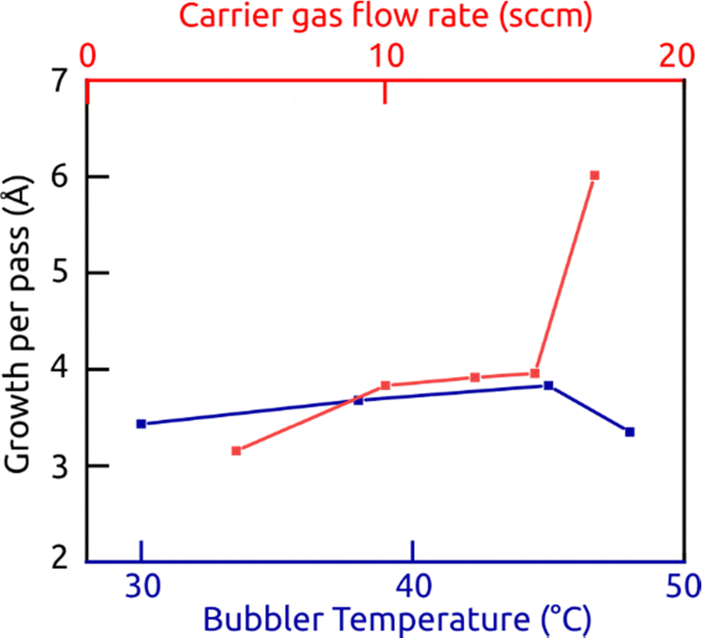 | ||
| Fig. 1 Self-limiting characteristics of the surface reaction characterized by varying the precursor dose in two distinct ways: variation of the carrier gas flow rate at a constant precursor and deposition temperature (red datapoints), and variation of the precursor container temperature at a constant carrier gas flow rate and constant substrate temperature (blue datapoints). | ||
If the precursor temperature is set to 45 °C, varying the carrier gas flow rate from 5 sccm to 20 sccm yields a saturation behavior between 10 sccm and 15 sccm at approximately 153(±18) nm after 400 passes (or 3.7(±0.4) Å per pass, blue datapoints in Fig. 1). Increasing the flow beyond 15 sccm takes the process out of the self-limiting ALD regime with an increased apparent deposition rate and increased roughness of the deposit, likely caused by the breakdown of the concentric laminar flows needed between the nozzle and substrate for spatially separated delivery of precursors A and B. Taking 10 sccm as the standard inert gas flow rate, the precursor doses can also be varied by adjusting the bubbler temperature between room temperature and 55 °C (red datapoints in Fig. 1). The saturation behavior also obtained here confirms that the process is stable in the conditions for self-limiting chemistry as in ALD and ALAM. We note that the precursor canister temperature needed for ALAM growth is significantly lower than in ALD (45 °C vs. 65 °C as the standard values in our equipment), which leads to the much lower precursor consumption and more efficient use of it in ALAM.
Let us now determine the temperature window over which this self-limiting chemistry is maintained. Fig. 2 exhibits how the thickness of the ALAM lines increases with number of passes at three distinct temperatures, and summarizes the growth rates (expressed as growth per pass). The thickness increases linearly with the number of passes at temperatures between 150 °C and 250 °C, with the growth rate being the highest of the three temperatures at 200 °C (3.7(±0.4) Å per pass) and slightly lower at 250 °C (2.70(±0.07) Å per pass). At temperatures up to 100 °C and beyond 250 °C, deposition occurs in a poorly controlled, poorly reproducible manner. Therefore, we assess that 200–250 °C represents the practically useable ‘ALD window’, in agreement with literature precedents in the ALD field.9
 | ||
| Fig. 2 Growth characteristics in ALAM. (a) Linearity of growth: film thickness increases with number N of passes as it depends on the substrate temperature, determined by imaging ellipsometry using 6 wavelengths. (b) Temperature dependence of the thickness growth per pass determined from the data in (a). | ||
The morphology of these straight lines as determined by imaging ellipsometry corresponds to the expectations (Fig. 3). Some noise is generated by imperfections in the ellipsometry data modelling and fitting. The lines exhibit a flat profile with sharp edges and no deposited material detected beyond the pattern. A thickness profile along the length of the line (red curve) is constant along the length until the extremities, which exhibit half of the thickness. This feature is inherent to the nature of the ALAM process and the circular symmetry of the precursor delivery nozzle in patterns featuring a back-and-forth motion of the nozzle.7,8 It represents a very visual, simple additional confirmation of the self-limiting nature of the surface reactions noted before. The thickness profile across the length highlights the flat top of the deposit, again a typical ALAM feature that is in stark contrast to what other deposition methods would achieve. The profile taken in the perpendicular direction (that is, across the line, blue curve in Fig. 3) exhibits a less perfect behavior. In particular, it features a pronounced dip at the very center. This characteristic is reproducible. Even though we cannot pinpoint with certainty the exact mechanism for its appearance, we attribute it to flow dynamics underneath the precursor delivery nozzle. Phenomena such as the distribution of gas velocities and local partial pressures may influence the surface reactions in ways that deviate from the simplistic ALD model.10,11 However, even this imperfect thickness profile across the line importantly exhibits a shape that is mostly reminiscent of a square block profile with sharp edges, and very distinct from a classical Gaussian profile expected for growth in the absence of self-limiting surface chemistry.
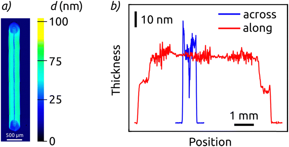 | ||
| Fig. 3 (a) Thickness map measured by imaging ellipsometry of an ALAM-printed SnO2 line (200 passes, 200 °C). (b) Thickness profiles extracted from (a) along the length of the line (red curve) and perpendicular to it (blue curve). The thickness shows a standard deviation of 1.4 nm along the 1521 data points in the central section of the length profile. | ||
Let us now turn to the characterization of the material obtained in our ALAM process. Microscopic investigation by scanning electron microscopy (SEM) and atomic force microscopy (AFM) suggests 200 °C as the optimal temperature, as it yields a continuous layer of reasonable roughness (the highest value being 9 nm RMS roughness for 400 passes or a nominal thickness of 152 nm, Fig. 4). The stoichiometry determined by energy-dispersive X-ray microanalysis (EDX) seems to become close to the nominal 1![[thin space (1/6-em)]](https://www.rsc.org/images/entities/char_2009.gif) :2 ratio of Sn and O in SnO2 beyond 200 °C (Fig. 4). At lower temperature, the amount of oxygen increases, indicating no SnO2−δ vacancies, but rather the formation of an amorphous oxide/hydroxide phase SnO2−a(OH)2a instead.
:2 ratio of Sn and O in SnO2 beyond 200 °C (Fig. 4). At lower temperature, the amount of oxygen increases, indicating no SnO2−δ vacancies, but rather the formation of an amorphous oxide/hydroxide phase SnO2−a(OH)2a instead.
 | ||
| Fig. 4 Morphology characterization of the ALAM-deposited SnO2 material. Top, scanning electron micrographs (10k magnification); center, topography, atomic force micrographs (5 × 5 μm2); lower line, atomic force micrographs phase image and EDX analyses (bar graphs at bottom). The 3 columns represent results obtained with deposition at 150 °C (a), 200 °C (b) and 250 °C (c), 400 passes all. | ||
This impression is confirmed by X-ray diffraction datasets collected in grazing-incidence geometry (GIXRD) on samples featuring square deposits of approximately 3 mm × 3 mm size made by ALAM rastering (400 passes). All samples deposited in the range of 60 to 295 °C yield no diffraction peaks (Fig. S1 in the ESI†). After annealing at 500 °C for 1 hour in air or nitrogen, however, all samples yield the diffraction peaks expected of crystalline SnO2 (cassiterite) in GIXRD (Fig. 5 and Fig. S1 in the ESI:† [110] near 26°; [101] near 34°; [111] and [200] near 37°; [211] near 52°; [220] near 54°), confirming the crystal structure of the annealed samples.
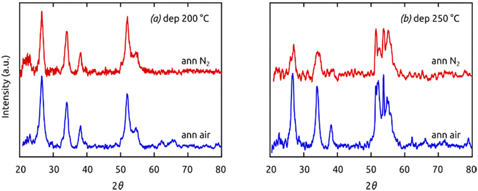 | ||
| Fig. 5 X-ray diffraction data collected in grazing incidence geometry for ALAM-deposited SnO2 squares (3 × 3 mm2, 400 passes) deposited at various temperatures, after annealing at 500 °C in nitrogen (red) or air (blue). | ||
Transmission electron microscopy (TEM) yields a finer degree of insight into the crystallinity and morphology (Fig. 6). For TEM studies, thin films for investigation have to be printed on electron transparent membranes (see Method section). Given the space between the heated sample stage and the window on which deposition occurs, the local temperature of the substrate is consequentially lower than that of the stage, so that the (nominal) stage temperature must be set to a value higher than in standard conditions (here, we use 250 °C). The diffuse halo rings in selected-area electron diffraction (SAED) confirm that the ALAM-printed line is amorphous as deposited (Fig. 6a). The Z-contrast STEM-HAADF images reveal that the deposited film is almost a compact thin film (Fig. 6c) on the SiNx membrane windows, consistent with the SEM and AFM results of printed lines on a solid substrate. The amorphous phase persists upon in situ annealing up to about 460 °C in the vacuum of TEM. Upon further increasing the annealing temperature in the TEM up to 540 °C, cracks in the film are observed (Fig. 6d). SAED revealed a transformation to the crystalline phase exhibiting the typical sharp powder diffraction ring pattern, which perfectly fits the pattern simulated for cassiterite (Fig. 6b). High-resolution TEM (HRTEM) lattice image (inset in Fig. 6d) analysis indicates that the particles have a size of approximately 10 nm.
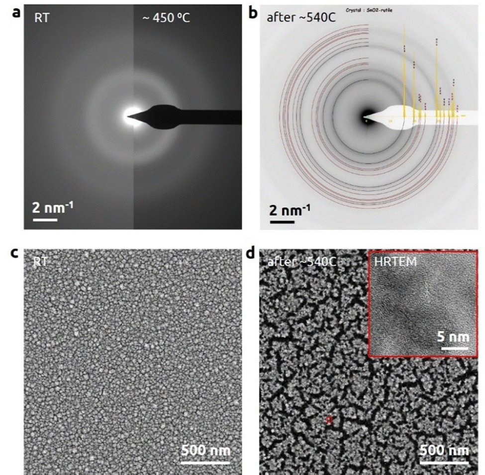 | ||
| Fig. 6 (In situ) TEM study of an ALAM-printed tin oxide thin film on a TEM SiNx membrane grid. (a) and (b) Selected-area electron diffraction (SAED) of the film during annealing at ∼450 °C (a), displaying halo rings typical of an amorphous structure, and at room temperature after annealing at ∼540 °C in the TEM (b), featuring a diffraction pattern with broad peaks indicative of crystalline nanoparticles (cassiterite phase, ICSD #9163, overlay). The contrast is inverted for better visualization of the simulation overlays. (c) and (d) STEM-HAADF (z-contrast images) images reveal the morphology of the thin film before (c) and after the annealing (d). A high-resolution micrograph is shown as the inset showing the lattice fringes in SnO2 nanoparticles of about 10 nm diameter. | ||
Conclusions
These results highlight the possibility of transferring thin film deposition chemistry from conventional ALD to ALAM. The self-limiting surface chemistry is demonstrated by a growth rate that is independent of precursor dose and by a linear thickness increase with number of passes. The line extremities featuring half thickness due to the U-turn motion provide an additional piece of evidence. Deposits of approximate SnO2 composition are obtained over the temperature window between 200 °C and 250 °C, but are amorphous as deposited. They crystallize upon annealing to 500 °C.ALAM delivers straight lines, raster rectangles and if needed further patterns featuring a mostly block profile in the absence of any lithographic patterning. It consumes minute amounts of precursors and does not generate the waste associated with the various lithographic process steps. We envision that such features will be of high interest towards the manufacture of miniaturized devices including embedded sensors. The next steps towards this goal will entail a systematic electrical characterization of ALAM-SnO2 lines.
Author contributions
Sonja Kürten: investigation, data curation, writing (original draft), writing (review and editing); Kimia Hashemizadeh: investigation, data curation; Mingjian Wu: investigation, data curation, writing (review and editing); Johannes Will: investigation, methodology; Ivan Kundrata: methodology; Erdmann Spiecker: methodology, supervision, funding acquisition, resources, writing (review and editing); Julien Bachmann: conceptualization, supervision, funding acquisition, resources, writing (review and editing).Data availability
All data presented in this article have been made available on the Zenodo platform. DOI: https://doi.org/10.5281/zenodo.14894088.Conflicts of interest
There are no conflicts to declare.Acknowledgements
We thank Prof. Marcus Halik (FAU) for use of his AFM. M. W., J. W. and E. S. acknowledge funding from the German Research Foundation (DFG) via the Research Training Group GRK 1896 “In situ microscopy with electrons, X-rays and scanning probes” and the Cluster of Excellence EXC 315 “Engineering of Advanced Materials” which made the in situ electron microscopy instrumentation available.Notes and references
- D. Wang, S. Liu, M. Shao, J. Zhao, Y. Gu, Q. Li, X. Zhang, J. Zhai and J. Fang, Ind. Eng. Chem. Res., 2018, 57, 7136–7145 CrossRef CAS.
- S. Chappel and A. Zaban, Sol. Energy Mater. Sol. Cells, 2002, 71, 141–152 CrossRef CAS.
- N. Sobel and C. Hess, Angew. Chem., Int. Ed., 2015, 54, 15014–15021 CrossRef CAS PubMed.
- C. Hägglund, T. Grehl, J. T. Tanskanen, Y. S. Yee, M. N. Mullings, A. J. M. Mackus, C. MacIsaac, B. M. Clemens, H. H. Brongersma and S. F. Bent, J. Vac. Sci. Technol., A, 2016, 34, 021516 CrossRef.
- B.-E. Park, J. Park, S. Lee, S. Lee, W.-H. Kim and H. Kim, Appl. Surf. Sci., 2019, 480, 472–477 CrossRef CAS.
- G. N. Parsons and R. D. Clark, Chem. Mater., 2020, 32, 4920 CrossRef CAS.
- I. Kundrata, M. K. S. Barr, S. Tymek, D. Döhler, B. Hudec, P. Brüner, G. Vanko, M. Precner, T. Yokosawa, E. Spiecker, M. Plakhotnyuk, K. Fröhlich and J. Bachmann, Small Methods, 2022, 6, 2101546 CrossRef CAS PubMed.
- S. Stefanovic, N. Gheshlaghi, D. Zanders, I. Kundrata, B. Zhao, M. K. S. Barr, M. Halik, A. Devi and J. Bachmann, Small, 2023, 19, 2301774 CrossRef CAS PubMed.
- M. N. Mullings, C. Hägglund and S. F. Bent, J. Vac. Sci. Technol., A, 2013, 31, 061503 CrossRef.
- M. B. M. Mousa, C. J. Oldham, J. S. Jur and G. N. Parsons, J. Vac. Sci. Technol., A, 2012, 30, 01A155 CrossRef.
- D. Seghete, F. H. Fabreguette and S. M. George, Thin Solid Films, 2011, 519, 3612–3618 CrossRef CAS.
Footnote |
| † Electronic supplementary information (ESI) available: Fig. S1, comprehensive set of XRD data of samples deposited at various temperatures and before and after annealing in air and under N2. See DOI: https://doi.org/10.1039/d5ma00182j |
| This journal is © The Royal Society of Chemistry 2025 |