
 Open Access Article
 This Open Access Article is licensed under a
 Creative Commons Attribution 3.0 Unported Licence
The role of primary and secondary electrons in scanning transmission electron microscopy of hybrid perovskites: the CsPbBr3 case
P. E.
Trevisanutto
 *a,
S.
Taioli
b,
M.
Dapor
b,
C. S.
Allen
c and
G.
Teobaldi
d
*a,
S.
Taioli
b,
M.
Dapor
b,
C. S.
Allen
c and
G.
Teobaldi
d
aScientific Computing Department, STFC UKRI, Daresbury Laboratory, Warrington WA4 4AD, UK. E-mail: paolo.trevisanutto@stfc.ac.uk
bEuropean Centre for Theoretical Studies in Nuclear Physics and Related Areas (ECT*), Bruno Kessler Foundation, Trento, Italy and Trento Institute for Fundamental Physics and Applications (TIFPA), Istituto Nazionale di Fisica Nucleare, Italy
cElectron Physical Science Imaging Center, Diamond Light Source Ltd., Didcot OX11 0DE, United Kingdom and Department of Materials, University of Oxford, Oxford OX1 3PH, UK
dScientific Computing Department, STFC UKRI, Rutherford Appleton Laboratory, Didcot OX11 0QX, UK
First published on 28th April 2025
Abstract
High-resolution imaging has revolutionised materials science by providing detailed insights into the atomic structures of materials. Electron microscopy and spectroscopy rely on analysing backscattered and transmitted electrons as well as stimulated radiation emission to form structural and chemical maps. These signals contain information about the elastic and inelastic electron scattering processes within the sample, including collective and single electron excitations such as plasmons, inter- and intra-band transitions. In this study, ab initio and Monte Carlo simulations were performed to investigate the behaviour of high-energy primary and secondary electrons in scanning transmission experiments on CsPbBr3 nanosamples. CsPbBr3 is a perovskite material known for its high photoluminescence quantum yield, making it promising for applications in light-emitting devices and solar cells. This study investigates and estimates the reflection and transmission of primary and secondary electrons based on their kinetic energy, sample thickness and electron affinity. The spatial distribution and energy spectra of the secondary electrons are also analysed and calculated to understand their generation depth and energy dynamics. These findings provide a theoretical framework for the study of charge transport in perovskites and can help to optimise scanning microscopy techniques for the imaging and characterisation of advanced materials.
I. Introduction
Among the significant advances in analytical techniques for materials science, atomic resolution imaging is one of the most impactful. These methods have enabled detailed visualisation of the structures and morphology of nanomaterials, crystals and metal surfaces, as well as biological samples and tissues.1,2In transmission electron microscopy (TEM), a beam of high-energy electrons is passed through a very thin sample (∼100 nm) and interference between elastically scattered electrons is exploited to form an image. This approach enables high-resolution imaging down to the atomic resolution (∼0.1 nm) and allows the precise visualisation of atomic arrangements. TEM microscopes typically operate at electron energies of 80–300 keV, although atomic resolution has already been demonstrated at 30 keV3,4 and even 15 keV.5
In a scanning electron microscope (SEM), a focused beam of electrons is raster scanned across a sample, and nm resolution images of the surface are formed from the analysis of emitted secondary electrons (SE) and backscattered electrons (BSE). The resolution in a SEM is largely limited by the interaction volume of the detected radiation, which, in most cases, precludes the need for incident electron probes smaller than ∼1 nm. SEM microscopes typically operate at electron beam kinetic energies of 1–30 keV. Images in a SEM are generally formed by collecting secondary or backscattered electrons that originate from the top surface of the sample. Performing in a low voltage mode, SEM in transmission mode has advantages over TEM imaging (albeit with lower spatial resolution) due to the relatively low cost and simplicity of the SEM instrument6 and has applications in both the physical7 and biological8 sciences.
Scanning transmission electron microscopy (STEM) combines elements of SEM and TEM. A finely focused electron beam is raster scanned across a thin sample (∼100 nm), and scattered electrons are detected to form an image. At high incident electron energy and for thin samples, the interaction volume is small and the microscope resolution is primarily limited by the size of the incident electron probe, which, with modern aberration-corrected optics, can reach sub-Ångström dimensions. Together with other emissions such as Auger electrons which are used to characterise the surface elemental compositions and X-rays applied to determine bulk crystal structures, the SEM, TEM and STEM represent the main techniques to analyse chemical composition and structure of materials.9
In high-resolution STEM and TEM experiments, a projection image is acquired, and it is challenging to obtain information on a sample variation along the beam direction. By placing SE detectors both before and after the sample within a STEM instrument, the surface sensitivity of SE detection can be exploited to determine the structure on both entrance and exit surfaces of a thin sample.10,11 This approach, to some extent, overcomes the projection limitation of the STEM.
A recent review12 has highlighted the applications for studying the dynamics and transient phenomena of surface reconstructions, exsolution of catalysts, lunar and planetary materials and the mechanical properties of 2D thin films utilising the simultaneous SE-STEM imaging.
Furthermore, inelastic scattering events within the sample, including SE generation,13 are a primary cause of electron beam-induced sample damage and need to be well understood to develop new approaches for imaging beam-sensitive materials. Motivated by the potential for transmitted SE imaging described in the above works, we construct a theoretical framework to calculate SE generation and emission in transmission through an industrially relevant metal-halide perovskite sample.
Any electron microscopy technique relies on electron scattering in the sample, which includes both elastic and inelastic processes. Both spectroscopic and SE imaging are products of inelastic scattering processes within the sample. These mechanisms are driven by energy loss phenomena, including single-particle electron excitations, collective atomic modes such as plasmons, electron–phonon and electron–polaron interactions, and Auger decay. Part of the energy loss contributes to the generation of a secondary electron cascade and, upon emission from the surface, to the secondary electron yield (SEY). Secondary electrons appear in the electron energy spectrum as a structured broad peak with energies below 50 eV. The emission of secondary electrons in SEM plays a decisive role in the formation of image contrast14 and can also lead to unwanted charge of the sample.15
Electron energy loss phenomena are influenced by two factors, namely the properties of the beam (i.e. kinetic energy, radiation type, and charge state) and the material properties, in particular the electronic excitation spectrum. The latter can be described by the so-called energy loss function (ELF), which can be obtained either from optical experiments or from EELS using a single scattering spectrum with the elastic peak and multiple scattering removed16 or via a reverse Monte Carlo (RMC) method.17 The ELF is a unique property of the material and is independent of the beam. However, it is difficult to interpret its spectral profile from the experiment alone, as the uniqueness of the ELF is not guaranteed by the fulfilment of the sum rules, i.e. the EELS signal can lead to different ELFs that all fulfil the sum rules18 and thus to different beam stopping properties. This emphasises the need for more precise theoretical descriptions and predictions of electron energy loss. In this context, ab initio calculations can also be used to determine the dielectric properties,19 especially in the low energy loss region.
In this article, the scattering behaviour of high-energy primary electrons (up to 50 keV, which covers the energy range of SEM and low energy TEM operation) and secondary electrons (up to 50 eV) in STEM experiments on CsPbBr3 thin films is theoretically investigated, using a mixed first-principles and Monte Carlo (MC) approach. In particular, linear response time-dependent density functional theory (LR-TDDFT) is used to calculate the ELF, while the MC routine models the charge transport in the solid. We have also investigated the reflection and transmission of primary and secondary electrons as a function of the kinetic energy of incidence and the sample thickness. Because electron microscopy (EM) samples are susceptible to beam-induced charging, we also determined the effects of the electron affinity (EA) on electron emission (we recall that the EA is measured from the bottom of the conduction band inside semiconductors and insulators). Finally, we determined the SE spectra and spatial distribution as functions of the initial kinetic energy of the primary beam by calculating the depth of secondary electron generation.
Caesium lead bromide, CsPbBr3, is an inorganic perovskite material that has attracted much attention in optoelectronics due to its high photoluminescence quantum yield (PLQY) with a sharp, narrow-band blue-green light emission.20–25 These properties make it a good candidate for industrial applications, e.g. in light-emitting devices (LEDs). As CsPbBr3 is a purely inorganic material, it is more stable under heat and less susceptible to degradation under harsh environmental conditions.26–28 Although CsPbBr3 has a relatively large bandgap (about 2.3 eV29), it can be used in tandem solar cells alongside silicon or other materials to cover different parts of the solar spectrum and increase overall efficiency. In addition, CsPbBr3 exhibits the “hot carrier effect”,30,31 in which excited electrons maintain high energy levels longer than in other materials, which has the potential to further increase the efficiency of solar cells. It has also shown the possibility of trion generation under high-energy laser excitation.32
II. Theory and methods
A. Energy loss function
The energy loss processes of electrons are described using Ritchie's dielectric theory.33,34 This approach is based on the knowledge of the macroscopic dielectric function![[small epsilon, Greek, macron]](https://www.rsc.org/images/entities/i_char_e0c6.gif) (q,ω), which can be calculated from first principles using LR-TDDFT or obtained from optical experiments. The former allows for the inclusion of momentum dispersion, which is necessary for the calculation of the stopping properties of materials, with the same computational effort as in zero-momentum transfer, whereas the latter approach must be extended to finite momentum by analytical dispersion laws, which are known to be valid only within certain limits.34 We have considered the orthorhombic geometric structure of CsPbBr3,29,35 which belongs to the crystallographic space group Pnma and is shown in Fig. 1.
(q,ω), which can be calculated from first principles using LR-TDDFT or obtained from optical experiments. The former allows for the inclusion of momentum dispersion, which is necessary for the calculation of the stopping properties of materials, with the same computational effort as in zero-momentum transfer, whereas the latter approach must be extended to finite momentum by analytical dispersion laws, which are known to be valid only within certain limits.34 We have considered the orthorhombic geometric structure of CsPbBr3,29,35 which belongs to the crystallographic space group Pnma and is shown in Fig. 1.
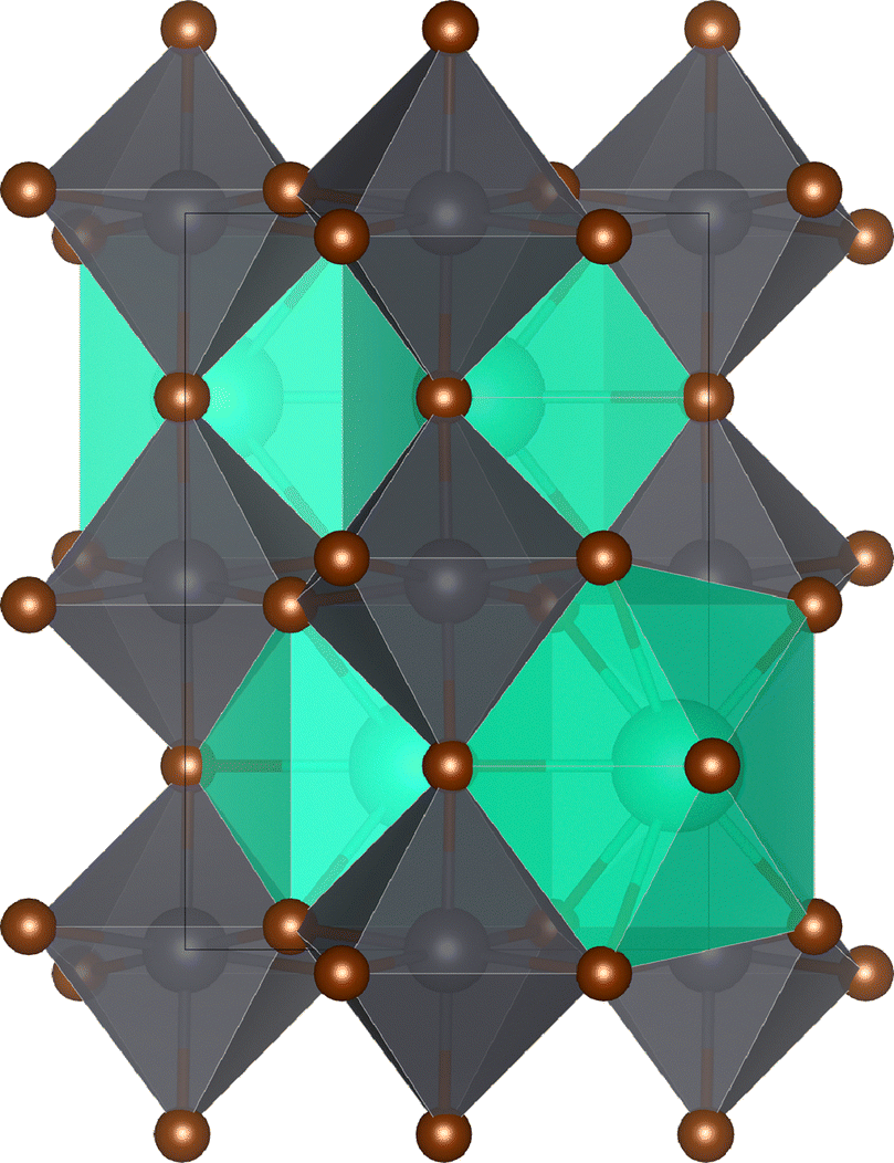 | ||
| Fig. 1 Geometric structure of CsPbBr3 (crystallographic space group Pnma) optimised by using density functional theory. Br is shown in brown and surrounds Pb (grey) and Cs (green) atoms. | ||
The electronic structure in the ground state was relaxed in the framework of density functional theory (DFT) using the generalised gradient approximation (GGA) of the exchange–correlation functional as implemented in the quantum espresso (QE) code suite.36 We have checked the convergence of the DFT parameters given in the literature.35,37,38 We note that the DFT and LR-TDDFT QE calculations performed under the random phase approximation (RPA) neglecting local field effects (RPA-NLFE) were compared with the same calculations using Elk,39 an all-electron full-potential linearised augmented plane-wave (LAPW) code and Questaal.40 The RPA-LFE LR-TDDFT calculations were performed with the Liouville–Lanczos turboEELS code.41 We have converged our k-mesh grid to 21 × 21 × 21 points.
In the LR-TDDFT, the susceptibility function χ(q,ω) can be obtained by solving the following Dyson-like equation:
| χ(q,ω)−1 = χ(q,ω)0−1 − vC(q) − fxc(q,ω), | (1) |
| ε(q,ω) = 1 − vC(q)χ(q,ω). | (2) |
In a periodic crystal, the microscopic dielectric function is denoted in reciprocal space as εG,G′(q,ω) ≡ ε(q + G, q + G′,ω), where G and G′ are reciprocal lattice vectors. The macroscopic dielectric function (or dielectric matrix) is related to the microscopic dielectric function by the following expression:
| (q,ω) = [ε−1]G=0,G′=0−1(q,ω). | (3) |
If this relationship is applied to the momentum q → 0 in the first Brillouin zone is referred to as the “optical limit”. The inversion of ε−1 with G and G′ not equal to zero leads to the inclusion of the so-called local field effects (LFE), which take into account the inhomogeneity of the system, in contrast to the non-local field effect (NLFE), in which only the head of the matrix is inverted. Using eqn (3), the ELF can be written as:
 | (4) |
To determine the effects of the AGGA correlation, the RPA (fxc(q,ω) = 0) is also used within LFE and NLFE. In the upper panel of Fig. 2 the ELFs are compared in the context of AGGA, RPA-LFE and RPA-NLFE. As we are currently unable to compare our computer simulations with the experimental results, the peaks are convolved with a typical Gaussian broadening of 0.1 eV. When RPA-LFE is compared with RPA-NLFE, a dramatic change in the shape of the ELF can be observed due to inhomogeneities. At the same time, the electron correlation in the AGGA kernel slightly increases the intensity in the 15–25 eV range, especially the 16.75 and ∼22 eV peaks, compared to RPA-LFE. The first less bright peak at 5 eV in the AGGA and RPA-LFE spectra is associated with the transition from the 4p states of the Br atom to the 6p states of Pb. The rich peak structures beyond 6 eV are primarily caused by transitions from the 4p states of the Br atom to a combination of 6p states of Cs and 6p states of Pb.
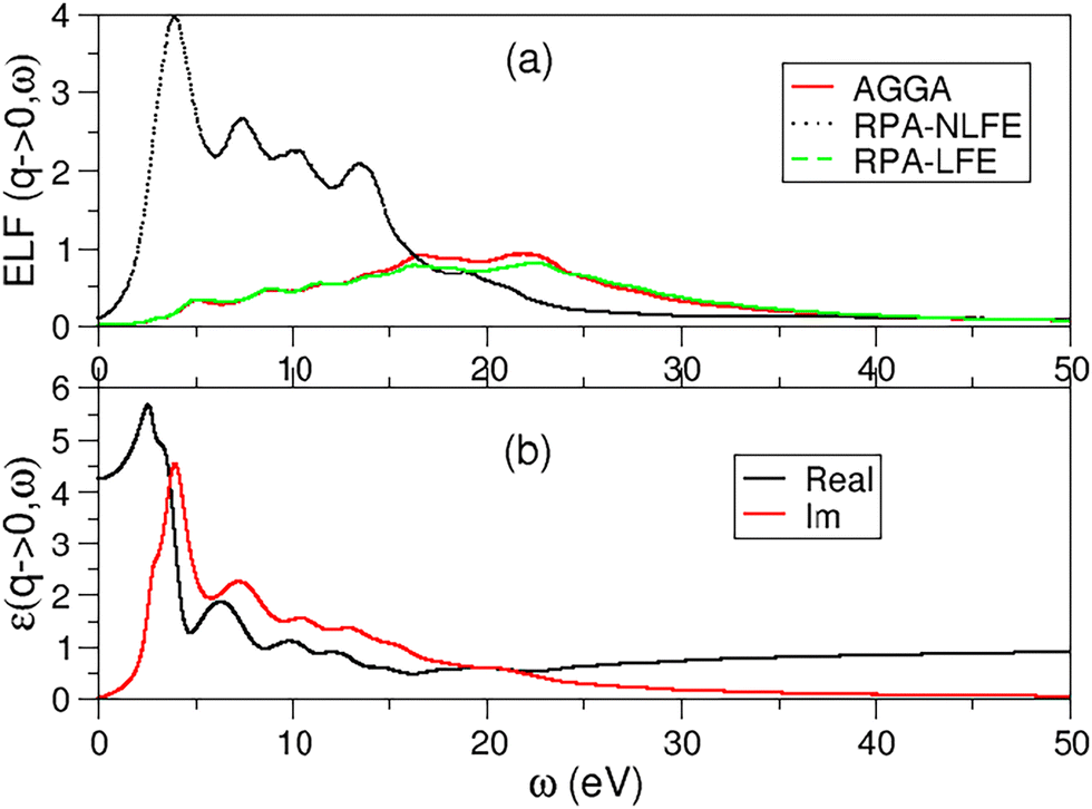 | ||
| Fig. 2 (a) ELF(q → 0,ω) of CsPbBr3 in RPA-NLFE (dotted black line), RPA-LFE (dashed green line) and AGGA (red solid line). (b) The real (black solid line) and imaginary (red solid line) parts of the dielectric function are calculated using LR-TDDFT within the AGGA framework. | ||
The real and imaginary parts of the dielectric function calculated using LR-TDDFT within the AGGA framework are shown in the bottom panel of Fig. 2. By analysing their spectral behaviour, it can be concluded that the 22 eV peak is associated with a mixed-state plasmon (the real part of the dielectric function remains positive, even if it is almost zero). In view of these results, we decided to use the TDDFT AGGA ELF, which contains the LFE, for our analysis.
In Fig. 3 the TDDFT AGGA LFE ELF is merged with the experimental form factors from the NIST datasets.43 This merging is necessary as the estimation of the high-energy TD-DFT ELF is computationally too demanding because of the numerous excited states that must be included in the calculation. On the other hand, the extension from 100 eV to 400 keV, which is related to the atomic core-level excitations, is needed to accurately determine the total inelastic cross section.
 | ||
| Fig. 3 ELF of CsPbBr3 in LR-TDDFT LFE AGGA merged with the ELF derived from the experimental form factors of the NIST datasets.43 | ||
B. Total inelastic scattering cross section and mean free path
To calculate the differential inverse inelastic mean free path (DIIMFP), which is used in our MC algorithm, we need to extend the ELF in the optical limit to finite momentum transfer q to account for energy-momentum dispersion. We have opted for the Drude–Lorentz approximation, where the dispersion is typically assumed to be a square law34 (see Appendix for details). The equation for the inverse inelastic mean free path (IIMFP), from which the total inelastic scattering cross section can be derived, is given by | (5) |
 are obtained by the energy-momentum conservation laws, a0 is the Bohr radius, m is the electron mass, and according to Ganachaud and Mokrani Wmin is the band gap and Wmax corresponds to the maximum energy of the incident electrons.44 We have tested that the relativistic effects on the IMFP of CsPbBr3 are minimal by performing the calculations with the relativistic extension of eqn (5)45 (the maximum kinetic energy considered in this work is ∼1/10 of the rest mass of the electron). Fig. 4 shows the IMFP (λinel) for CsPbBr3 as a function of the electron kinetic energy.
 | ||
| Fig. 4 IMFP (Å) as a function of the kinetic energy of the incident electron (eV), obtained by extending the ELF from TDDFT-AGGA in the energy axis via the NIST datasets and in the momentum transfer axis q according to the quadratic dispersion law.34 The minimum of the IMFP is 5.34 Å for an energy of 57 eV. | ||
C. Total elastic scattering cross section and mean free path
Elastic scattering is accounted for in our MC approach using Mott theory, which we have generalised to account for the presence of multiple scattering between neighbours in the periodic unit cell.46 In this approach, the differential elastic scattering cross section (DESCS) for an electron scattered by a central atomic potential at an angle θ is as follows: | (6) |
 | (7) |
![[thin space (1/6-em)]](https://www.rsc.org/images/entities/char_2009.gif) sinθ′dθ′.
sinθ′dθ′.
III. Monte Carlo results
Since we have access to the cross sections of elastic and inelastic scattering, our MC algorithm works as follows:34,47 we extract a random number μ that is sampled from a uniform distribution in the interval [0,1] and use it to determine the step length that each electron travels within the solid target Δs = −λln(μ), where λ is the mean free path that includes all elastic (λel−1) and inelastic (λinel−1) scattering processes and can be calculated from λ−1 = λel−1 + λinel−1.
Finally, the MC method selects an elastic or inelastic scattering event by comparing another random number μ′, which is sampled from a uniform distribution in the range [0, 1], with the corresponding probability. If μ′ ≤ λel−1/λ−1, it is an elastic scattering event that leads to an angular deviation of the electron's trajectory; otherwise, the electron suffers an inelastic interaction that leads to both energy loss and (typically small) angular deviation.47 We note that to escape from the surface of the sample, the electrons must overcome the barrier at the interface between the vacuum and the solid, i.e. they must fulfill the condition Ecos2(ϑ) ≥ EA where ϑ is the angle formed between the surface normal and the intersection of the electron trajectory on the surface, and E is the kinetic energy of the electrons. In addition, the transmission from solid to vacuum is modeled by a transmission coefficient that depends on the EA of the material.34
A. Reflection electron energy loss spectrum (REELS)
Using the MC approach described above, we have calculated the reflection electron energy loss spectrum (REELS)48 for different initial energies of the incident electrons (black solid line for 10 keV kinetic energy, red line for 20 keV, green line for 30 keV, orange line for 40 keV, and blue line for 50 keV), as shown in Fig. 5. Part of the electrons of the primary beam can be backscattered with the same energy as the incident energy and represents the so-called elastic (or lossless) peak, which typically also hides substructures due to electron–phonon scattering. We performed all MC calculations with a total number of electrons equal to 1010 to obtain a good signal-to-noise ratio. | ||
| Fig. 5 Monte Carlo simulation of the reflection energy loss spectrum (Reels) of electrons emerging from a 100 nm thick CsPbBr3 sample for different kinetic energies of the primary beam: 10 (black line), 20 (red line), 30 (green line), 40 (orange line) and 50 (blue line) keV. The inset shows the plasmon peak for a 20 keV electron beam. | ||
The elastic peaks shown in Fig. 5 are extremely bright and lie at the initial kinetic energy of the primary beam. The energy loss spectra show several peaks reflecting the ELF lineshape. In Fig. 5, the inset image highlights the first 100 eV of energy loss for an initial impact energy of 20 keV. The shoulders in the 20 keV REELS at 5, 8 and 12 eV from the elastic peak are directly related to single-particle excitations (Br 4p states → Pb 6p states and Br 4p states → Cs 6p states), which also occur in the ELF. The highest peak is at 22 eV away from the elastic peak, which is a mixed single-electron/plasmon transition.
B. Backscattered electrons
To investigate the effects of the film thickness on the reflected electrons, we also calculated the backscattering coefficient ηB (i.e. the fraction of backscattered electrons to total electrons) as a function of incident electron energies of 5, 10, 15, 20, 30, 40 and 50 keV. In Fig. 6 we show the results for three CsPbBr3 thin films of thickness 50 (cyan coloured line with full circles), 100 (black coloured line with full squares) and 200 nm (magenta coloured line with full diamonds). The backscattering coefficients for the CsPbBr3 sample exhibit a monotonically decreasing trend with increasing kinetic energy, which depends on the sample thickness; in particular, for a given initial kinetic energy of the primary electrons, the reflection is higher for thicker samples and is almost zero at 50 keV, i.e. all electrons are transmitted. At 5 keV, the reflection rate for the 200 nm sample is more than twice as high as for the 50 nm sample (ηB = 0.52 compared to ηB = 0.22, respectively). The intensities of the elastic peaks in Fig. 5 show the decisive contribution of the elastic collisions to the backscattering coefficient.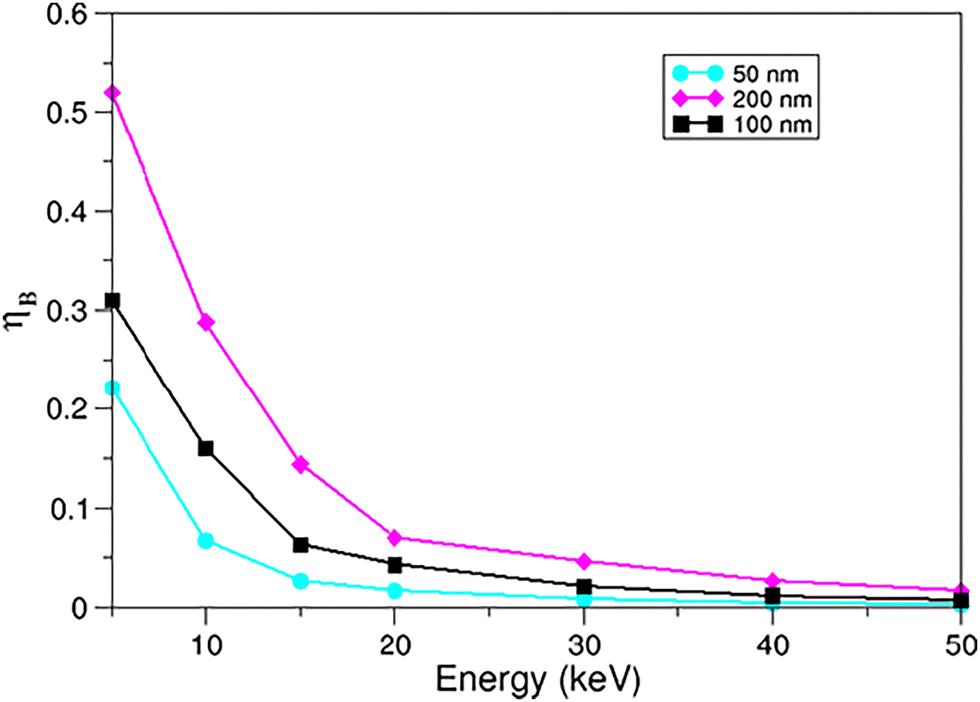 | ||
| Fig. 6 Backscattering coefficient (ηB) for the electrons of the primary beam as a function of their initial kinetic energy (keV). The results are shown for three different sample thicknesses: 50 nm (cyan-coloured solid line), 100 nm (black solid line) and 200 nm (magenta-coloured solid line). | ||
C. Secondary electrons
Electron beams that hit a material can also trigger the emission of secondary electrons by depositing their kinetic energy in the target. These electrons are emitted by the atoms of the solid as a result of inelastic interactions with the target, which may involve either the primary beam or other secondary electrons. The yield of transmitted or reflected secondary electrons recorded by the detector is influenced by all kinds of inelastic interactions with individual and collective charges, such as Auger decay, phonons, plasmons, trapping and charge density waves (CDW). Secondary electron emission is the primary contrast mechanism in an SEM and in SE imaging within the TEM. Secondary electron generation can also contribute to the charging of a sample, which has implications on electron beam-induced damage mechanisms.10,11,13,49 In this context, the SE yield is defined as the ratio between the number of secondary electrons (reflected or transmitted with a kinetic energy below 50 eV, although secondary electrons above this nominal limit can also be found) and the total number of primary electrons. The secondary yield is thus defined per incident particle.In Fig. 7 we show the yield of reflected secondary electrons δ determined for different initial kinetic energies of the primary electron beam of 1, 2, 5, 10, 20, 30, 50 keV for thicknesses of 50 (cyan line), 100 (black lines) and 200 nm (magenta line) for EA = 4.1 eV (pristine material). To investigate the dependence of the yield on the EA, which may depend on surface termination and material history, calculations were also performed for EA = 3 eV (black dash-dotted line) and 5 eV (black dashed line) and 100 nm thickness.
 | ||
| Fig. 7 Reflection yield of the secondary electrons (δ) as a function of the kinetic energy of the primary beam (keV). The results are shown for three different sample thicknesses and electron affinities: 50 nm (cyan-coloured solid line), 100 nm (black solid line) and 200 nm (magenta-coloured solid line) for EA = 4.1 eV (pristine material). For the 100 nm layer, results with EA = 3.0 eV (black dash-dotted line) and 5.0 eV (black dashed line) are also included. | ||
The reflection yield of secondary electrons decreases with increasing initial kinetic energy, from which we can conclude that low-energy primary electrons have a greater chance of producing the escaping secondary electrons immediately below the target surface. The secondary reflection at low kinetic energy of the incident electrons shows a behaviour that is almost independent of the sample thickness, in contrast to the backscattering coefficient of the reflected primary electrons. In addition, the EA plays a fundamental role in increasing the production of secondary electrons. At low kinetic energy of the primary beam, an EA = 3 eV leads to increased production of secondary electrons, while an EA = 5 eV attenuates them. This is particularly evident at the lowest energies (e.g. 2 and 5 keV) and confirms that impinging electrons with lower kinetic energy have a higher probability of emitting secondary electrons. At odds, the electrons penetrate deep into the sample at the high energy of the primary beam (50 keV) and the generated secondary electrons cannot escape at the vacuum-target interface due to the numerous inelastic scatterings they suffer on their way out of the solid; in this case, the different EAs have little influence on the secondary reflection yield.
In Fig. 8 the secondary electron energy (ΔEnergy = E − Evac, with Evac the near-surface vacuum energy) spectra are shown as a function of the initial kinetic energy of the primary beam equal to 1 (orange solid line), 2 (black solid line), 5 (red solid line), 10 (green solid line), 20 (blue solid line) and 50 keV (cyan solid line) for three different thicknesses of 50 (left), 100 (centre), 200 nm (right). The resulting secondary electrons are distributed over a range of 25 eV with a sustained peak at around 2.6 eV for all layer thicknesses and kinetic energies of the primary beam. These lineshapes are consistent with the secondary kinetic energy spectra obtained by real-time TDDFT (RT-TDDFT) calculations for graphene, where a peak position at 3.5 eV50 with an EA = 4.56 eV was found, for semiconductor materials such as TiN, VN, GaAs, InAs, InSb, PbS using the reverse MC approach,51 and with the analytical expression for metals originally developed by Chung–Everhart,52 which relates the position of the secondary electron peak to the EA. The Chung–Everhart expression can also be used to estimate grossly the peak distributions for non-metals. Considering the CsPbBr3 EA = 4.1 eV, the Chung–Everhart formula provides a peak position measured from the vacuum level at 1/3 of the EA, i.e. 4.1/3 ≃ 1.36 eV (≃ 1.3 eV below our estimate). Nevertheless, in our simulations, we confirm a red (blue) shift of the peak position by 0.3 eV for an EA of 3.0 eV (5.0 eV). At a thickness of 100 nm (centre panel of Fig. 8), the positively charged sample (EA = 3 eV, dotted-dashed line) enhances the intensity of the spectra of the kinetic energy of the secondary electrons, while the EA = 5 eV (corresponding to negatively charged samples, dashed line) attenuates it.
 | ||
| Fig. 8 Spectral distribution (with respect to the vacuum energy ΔEnergy = E − Evac, eV) of the reflected secondary electrons, parameterised for different initial kinetic energies of the primary electrons for three-layer thicknesses of 50 (left), 100 (centre) and 200 nm (right). For the 100 nm thick layer, the electron distribution was also calculated for an EA of 3.0 eV (dotted–dashed lines) and 5.0 eV (dashed lines), while the solid lines represent the pristine CsPbBr3 (EA = 4.1 eV). The coloured lines represent the different initial kinetic energies of the primary beam of 1 (orange lines), 2 (black lines), 5 (red lines), 10 (green lines), 20 (blue lines), 30 (magenta lines) and 50 keV (cyan lines). | ||
The conclusions that can be drawn from these results for the reflected secondary electron yield are as follows: (i) the more intense secondary electron distributions are found for low kinetic energies (5–10 keV) of the primary electrons rather than for higher energies (e.g. 50 keV). (ii) The EAs influence the distributions of the secondary electron yield mainly at low kinetic energies of the primary electrons (with a maximum at 2.6 keV). (iii) The distributions are not significantly influenced by the thickness of the layer.
D. Transmission of the primary and secondary electrons
The analysis carried out for the backscattered electrons is repeated for the primary and secondary electron transmission. In Fig. 9, the transmission coefficient (ηT) is plotted against the initial kinetic energies of the primary beam for three thicknesses. The number of transmitted primary electrons per incident particle is always less than 1 at low kinetic energy, as a large fraction of the incident electrons are reflected. However, the primary transmission coefficient saturates at a higher kinetic energy (>30 keV) for all investigated samples. We also note that the transmission coefficient decreases with increasing thickness at all energies. In particular, for the 100 nm thick layer (black solid line), the transmission coefficient of the primary electrons shows a behaviour between 50 (cyan solid line) and 200 nm (magenta solid line). In the case of 50 nm (cyan solid line), the primary electrons are almost completely transmitted at an incident energy of 5 keV. We emphasise that the spectra and yield of the secondary electrons, which are typically orders of magnitude greater in number than the primary electrons, have a better signal-to-noise ratio than the corresponding magnitudes of the primary electrons. | ||
| Fig. 9 Transmission coefficient (ηT) for the primary electrons as a function of the initial electron kinetic energy (keV). The results are shown for three different sample thicknesses: 50 nm (cyan solid line), 100 nm (black solid line) and 200 nm (magenta solid line). | ||
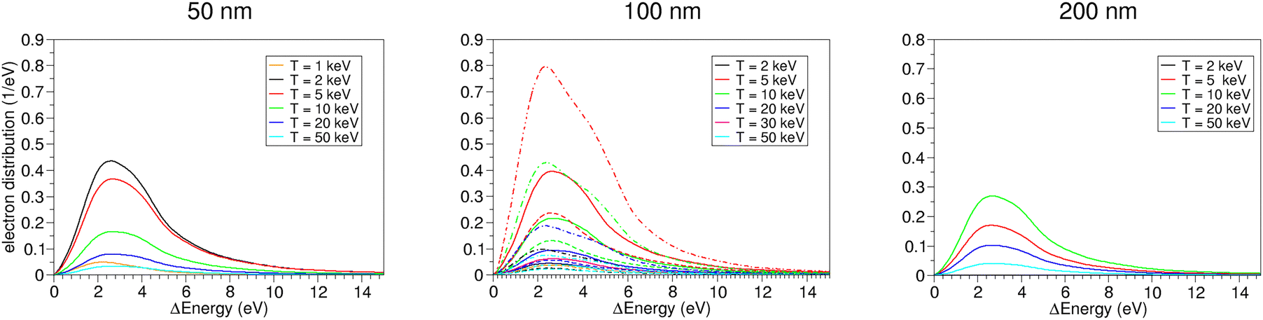
The transmission coefficient of the secondary electrons as a function of the primary beam kinetic energy reported in Fig. 10 shows a maximum, whose position and intensity depend on the thickness: 2 keV for 50 nm (cyan solid line), 5 keV for 100 nm (black solid line) and 10 keV for 200 nm (magenta solid line). We also find that the intensity of the maximum of δT decreases with increasing thickness and the EA also significantly affects the intensity of the transmitted secondary electrons; in particular the higher the EA, the smaller δT. We attribute this result to the fact that the only secondary electrons that can escape are those that originate near the vacuum interface (opposite the entrance surface). This behaviour can be interpreted in the light of Fig. 11, where we plot the distribution of transmitted secondary electrons as a function of origin depth. Fig. 11 shows that the number of generated secondary electrons initially increases as the energy of the primary electrons increases. However, this trend reverses as soon as the energy exceeds a certain threshold value, which is determined by the thickness of the film. This leads to a saturation point at which a considerable number of electrons from the primary beam pass through the film without much interaction and no longer contribute to the production of secondary electrons. This is also reflected in the thickness-dependent plateau in Fig. 9 for the transmission of primary electrons (>30 keV). Moreover, we find that the maximum secondary electron transmission occurs at a depth of about 0.75 nm along the direction of incidence from the interface to the vacuum. Finally, we also note that the generation of secondary electrons is filtered out at a low initial kinetic energy of the primary beam, e.g. the 2 keV distribution is most intense in a 50 nm thick layer, while it is attenuated in the 100 nm thick layer and suppressed in the 200 nm thick layer.
 | ||
| Fig. 10 Secondary electron transmission yield (δT) as a function of the initial kinetic energy of the primary beam (keV). The results are shown for three different sample thicknesses and electron affinities: pristine material (EA = 4.1 eV), 50 nm (cyan solid line), 100 nm (black solid line) and 200 nm (magenta solid line). The results for a depth of 100 nm with EA = 3.0 eV (black dashed line) and 5.0 eV (black dashed line) are also shown. | ||
 | ||
| Fig. 11 Distribution of transmitted secondary electrons as a function of the origin depth (along z-axis, in nm), parameterised for different initial primary electron energies for slab thicknesses of 50 (left), 100 (centre) and 200 (right) nm, respectively. The initial kinetic energies of the primary electron beam are T = 1 keV (orange lines), 2 keV (black lines), 5 keV (red lines), 10 keV (green lines) and 20 keV (blue lines). | ||
Finally, Fig. 12 shows the energy distributions of the transmitted secondary electrons for different parametrised layer thicknesses. Similar to the behaviour of the reflected secondary electrons, the energy spectra of the transmitted secondary electrons also exhibit a persistent peak around 2.6 eV, independent of the thickness and kinetic energy of the primary beam, with a tail reaching up to 20 eV. EA of 3 (5) eV increases (attenuates) the intensity of the peaks and produces a small red (blue) shift in the peak position, as shown in the centre panel of Fig. 12. The EA affects the transmission yield of secondary electrons, even at a kinetic energy of 50 keV.
 | ||
| Fig. 12 Energy spectra of the transmitted secondary electrons as a function of the kinetic energy of emission (with respect to the vacuum energy ΔEnergy = E − Evac, eV) for different initial primary electron energies for the three slab thicknesses, namely 50 (left), 100 (centre) and 200 (right) nm. For the 100 nm slab, the electron distribution was also calculated with an EA of 3.0 eV (dotted-dashed lines) and 5.0 eV (dashed lines), while for the original CsPbBr3 the EA is 4.1 eV (solid lines). The initial kinetic energies of the primary beam are T = 1 keV (orange lines), 2 keV (black lines), 5 keV (red lines), 10 keV (green lines), 20 keV (blue lines), 30 keV (magenta lines) and 50 keV (cyan lines). | ||
IV. Discussion and conclusions
In this study, we have theoretically investigated the scattering processes of high-energy primary and secondary electrons expected from scanning transmission electron microscopy measurements of the perovskite CsPbBr3. To this end, we used MC simulations in combination with first-principles LR-TDDFT calculations of the electron loss function to determine the inelastic mean free path of bulk CsPbBr3.We have focused in particular on analysing the reflection and transmission properties of backscattered and secondary electrons by calculating the spectra and yields of the emitted secondary electrons in thin films of CsPbBr3.
In terms of reflection, our results show that the backscattering coefficient of primary electrons decreases monotonically with kinetic energy and increases with film thickness. For secondary electrons, the EA (and not the thickness) plays a decisive role in the emission of these electrons, i.e. the higher the EA the lower their emission, although its influence diminishes at higher energies.
In terms of transmission, the observed peaks depend on both the thickness of the material and the initial kinetic energy of the primary electrons. In general, the transmission coefficient of primary electrons is greater for thinner films and approaches unity for initial kinetic energies of the primary beam above 30 keV for all thicknesses investigated. Transmitted secondary electrons are most likely to be emitted when they are generated within the last 10 nm of the nanolayer. In particular, the number of transmitted secondary electrons, which, as with reflection, reacts very sensitively to the EA, depends strongly on the layer thickness and the kinetic energy of the primary electrons: Initially, it increases sharply with the kinetic energy of the primary electrons for all layer thicknesses up to a thickness-dependent maximum and then decreases monotonically, as electrons that are too energetic cannot generate secondary electrons and are simply transmitted without causing emissions.
These results contribute to a better understanding of the transmission and reflection characteristics of primary and secondary electrons, ultimately aiding in the quantitative interpretation of the electron intensity in STEM experimental measurements.
Data availability
The data supporting the findings of this study will be publicly available at https://github.com/stfc/ALC_SUTOR. Additional details regarding data access and restrictions can be obtained by contacting the corresponding author.Conflicts of interest
There are no conflicts to declare.Appendices
A: Drude–Lorentz method
The inelastic scattering cross section is derived from the ELF in the entire spectrum of excitation energies (ω) and momentum transfers q. While first-principles methods can effectively determine the ELF for energies below 100 eV, performing ab initio calculations of the ELF over such a broad energy range (up to 400 keV) is often prohibitively expensive due to the enormous number of excited states that must be included in the ELF calculation. To obtain the IMFP in the investigated energy range, we need to rely on experimental NIST X-ray atomic data (TDDFT-NIST).43The TDDFT-NIST ELF was first fitted using the ALC_SUTOR suite,53 which uses nonlinear least squares minimisation lmfit.54 We used 34 Drude–Lorentz oscillators with a momentum-dependent broadening parameter γi as follows:
 | (A1) |
 | (A2) |
To include the electronic excitations of the inner shells in the ELF calculation, we have additionally used 10 Fano functions and 4 power-law functions that accurately reproduce the sharp edges associated with the core excitations.
The result of this fitting procedure is shown in Fig. 13. For details on different methods to extend the ELF beyond the optical limit, see ref. 34.
 | ||
| Fig. 13 Drude–Lorentz fit (black line) of the TDDFT-NIST43 ELF (red line). | ||
Acknowledgements
This work was supported by the Ada Lovelace Centre. The authors gratefully acknowledge the use of ARCHER2 (via the UK Car–Parrinello Consortium, EP/X035891/1) and the STFC-SCARF HPC facilities. S. T. acknowledges the European Union for funding under grant agreement no 10104665. P. E. T. thanks Dr J. Jackson for assistance with the Questaal calculations and Dr I. Scivetti for his help with Archer2.References
- A. Rivacoba, N. Zabala and J. Aizpurua, Image potential in scanning transmission electron microscopy, Prog. Surf. Sci., 2000, 65, 1 CrossRef.
- P. D. Nellist, Scanning transmission electron microscopy, in Springer Handbook of Microscopy, ed. P. W. Hawkes and J. C. H. Spence, Springer International Publishing, Cham, 2019, pp. 49–99 Search PubMed.
- H. Sawada, T. Sasaki, F. Hosokawa and K. Suenaga, Atomic-resolution stem imaging of graphene at low voltage of 30 kv with resolution enhancement by using large convergence angle, Phys. Rev. Lett., 2015, 114, 166102 CrossRef PubMed.
- C. S. Allen, M. Danaie, J. H. Warner, D. J. Batey and A. I. Kirkland, Super-resolution electron ptychography of low dimensional materials at 30 kev: Beyond the detector limit, Appl. Phys. Lett., 2023, 123, 023101 CrossRef.
- T. Sasaki, H. Sawada, F. Hosokawa, Y. Sato and K. Suenaga, Aberration-corrected stem/tem imaging at 15 kv, Ultramicroscopy, 2014, 145, 50 CrossRef PubMed , low-Voltage Electron Microscopy.
- T. Klein, E. Buhr and C. Georg Frase, tsem: A review of scanning electron microscopy in transmission mode and its applications, in Advances in Imaging and Electron Physics, Advances in Imaging and Electron Physics, ed. P. W. Hawkes, Elsevier, 2012, ch. 6, vol. 171, pp. 297–356 Search PubMed.
- J. Holm, Quantifying low-kev beam damage in ultrathin mfi zeolite nanosheets with an sem, Microsc. Microanal., 2022, 29, 131 CrossRef.
- M. Kuwajima, J. M. Mendenhall, L. F. Lindsey and K. M. Harris, Automated transmissionmode scanning electron microscopy (tsem) for large volume analysis at nanoscale resolution, PLoS One, 2013, 8, e59573 CrossRef PubMed.
- S. Taioli, S. Simonucci, L. Calliari and M. Dapor, Electron spectroscopies and inelastic processes in nanoclusters and solids: Theory and experiment, Phys. Rep., 2010, 493, 237 CrossRef.
- B. Plotkin-Swing, J. Martis, C. Su, M. T. Hotz, N. Dellby, T. Radlička, O. L. Krivanek and T. C. Lovejoy, Atomic resolution secondary electron imaging of top and bottom surfaces, Microsc. Microanal., 2024, 30, ozae044.731 CrossRef.
- O. Dyck, J. L. Swett, C. Evangeli, A. R. Lupini, J. Mol and S. Jesse, Contrast mechanisms in secondary electron e-beam-induced current (seebic) imaging, Microsc. Microanal., 2022, 28, 1567–1583 CrossRef CAS PubMed.
- M. L. San Gabriel, C. Qiu, D. Yu, T. Yaguchi and J. Y. Howe, Simultaneous secondary electron microscopy in the scanning transmission electron microscope with applications for in situ studies, Microscopy, 2024, 73, 169 CrossRef PubMed.
- H. Suzuki, Z. Akase, K. Niitsu, T. Tanigaki and D. Shindo, Secondary electron effect on electron beam induced charging of sio2 particle analyzed by electron holography, Microscopy, 2017, 66, 167 CAS.
- M. Dapor, M. Ciappa and W. Fichtner, Monte Carlo modeling in the low-energy domain of the secondary electron emission of polymethylmethacrylate for critical-dimension scanning electron microscopy, J. Micro/Nanolithogr., MEMS, MOEMS, 2010, 9, 023001 CrossRef.
- S. Taioli, M. Dapor, F. Dimiccoli, M. Fabi, V. Ferroni, C. Grimani, M. Villani and W. J. Weber, The role of low-energy electrons in the charging process of lisa test masses, Classical Quantum Gravity, 2023, 40, 075001 CrossRef.
- R. F. Egerton, Electron Energy-Loss Spectroscopy in the Electron Microscope, Springer, New York, Dordrecht, Heidelberg, London, 2011 Search PubMed.
- Z. Li, J. Gong, B. Da, J. Tóth, K. Töokési, R. Zeng and Z. J. Ding, Improved reverse monte carlo analysis of optical property of fe and ni from reflection electron energy loss spectroscopy spectra, Sci. Rep., 2023, 13, 12480 CrossRef CAS PubMed.
- P. de Vera, I. Abril and R. Garcia-Molina, Electronic cross section, stopping power and energy-loss straggling of metals for swift protons, alpha particles and electrons, Front. Mater., 2023, 10, 1249517 CrossRef.
- S. Taioli, P. Umari and M. M. De Souza, Electronic properties of extended graphene nanomaterials from gw calculations, Phys. Status Solidi B, 2009, 246, 2572 CrossRef CAS.
- S. Shi, Y. Wang, S. Zeng, Y. Cui and Y. Xiao, Surface regulation of cspbbr3 quantum dots for standard blue-emission with boosted plqy, Adv. Opt. Mater., 2020, 8, 2000167 CrossRef CAS.
- S. Wang, C. Bi, J. Yuan, L. Zhang and J. Tian, Original core-shell structure of cubic cspbbr3 amorphous cspbbr3 perovskite quantum dots with a high blue photoluminescence quantum yield of over 80%, ACS Energy Lett., 2018, 3, 245 CrossRef CAS.
- J.-S. Yao, J. Ge, B.-N. Han, K.-H. Wang, H.-B. Yao, H.-L. Yu, J.-H. Li, B.-S. Zhu, J.-Z. Song, C. Chen, Q. Zhang, H.-B. Zeng, Y. Luo and S.-H. Yu, Ce3-doping to modulate photoluminescence kinetics for efficient cspbbr3 nanocrystals based light-emitting diodes, J. Am. Chem. Soc., 2018, 140, 3626 CrossRef CAS PubMed.
- H. Guan, S. Zhao, H. Wang, D. Yan, M. Wang and Z. Zang, Room temperature synthesis of stable single silica-coated cspbbr3 quantum dots combining tunable red emission of ag-inzn-s for high-cri white light-emitting diodes, Nano Energy, 2020, 67, 104279 CrossRef CAS.
- S. Wei, Y. Yang, X. Kang, L. Wang, L. Huang and D. Pan, Room-temperature and gramscale synthesis of cspbx3 (x = cl, br, i) perovskite nanocrystals with 50–85% photoluminescence quantum yields, Chem. Commun., 2016, 52, 7265 RSC.
- Z.-J. Yong, S.-Q. Guo, J.-P. Ma, J.-Y. Zhang, Z.-Y. Li, Y.-M. Chen, B.-B. Zhang, Y. Zhou, J. Shu, J.-L. Gu, L.-R. Zheng, O. M. Bakr and H.-T. Sun, Doping-enhanced short-range order of perovskite nanocrystals for near-unity violet luminescence quantum yield, J. Am. Chem. Soc., 2018, 140, 9942 CrossRef CAS PubMed.
- D. Han, K. Yang, C. Bai, F. Chen, Z. Sun, Y. Wang, H. Ji, Z. Yang and X. Tang, Thermal and chemical durability of metal halide perovskite cspbbr3 single crystals, Chem. Eng. J., 2023, 475, 146209 CrossRef CAS.
- C. Bi, Z. Yao, X. Sun, X. Wei, J. Wang and J. Tian, Perovskite quantum dots with ultralow trap density by acid etching-driven ligand exchange for high luminance and stable pure-blue light-emitting diodes, Adv. Mater., 2021, 33, 2006722 CrossRef CAS PubMed.
- L. Protesescu, S. Yakunin, S. Kumar, J. Bar, F. Bertolotti, N. Masciocchi, A. Guagliardi, M. Grotevent, I. Shorubalko, M. I. Bodnarchuk, C.-J. Shih and M. V. Kovalenko, Dismantling the “red wall” of colloidal perovskites: Highly luminescent formamidinium and formamidinium-cesium lead iodide nanocrystals, ACS Nano, 2017, 11, 3119 CrossRef CAS PubMed.
- M. Ezzeldien, S. Al-Qaisi, Z. A. Alrowaili, M. Alzaid, E. Maskar, A. Es-Smairi, T. V. Vu and D. P. Rai, Electronic and optical properties of bulk and surface of cspbbr3 inorganic halide perovskite a first principles dft 1/2 approach, Sci. Rep., 2021, 11, 20622 CrossRef CAS PubMed.
- B. Yang and K. Han, Charge-carrier dynamics of lead-free halide perovskite nanocrystals, Acc. Chem. Res., 2019, 52, 3188 CrossRef CAS PubMed.
- P. Zeng, X. Ren, L. Wei, H. Zhao, X. Liu, X. Zhang, Y. Xu, L. Yan, K. Boldt, T. A. Smith and M. Liu, Control of hot carrier relaxation in cspbbr3 nanocrystals using damping ligands, Angew. Chem., Int. Ed., 2022, 61, e202111443 CrossRef CAS.
- Z. Cao, F. Hu, Z. Man, C. Zhang, W. Zhang, X. Wang and M. Xiao, Trion-facilitated dextertype energy transfer in a cluster of single perovskite cspbbr3 nanocrystals*, Chin. Phys. Lett., 2020, 37, 127801 CrossRef CAS.
- R. H. Ritchie, Plasma losses by fast electrons in thin films, Phys. Rev., 1957, 106, 874 CrossRef CAS.
- S. Taioli and M. Dapor, Advancements in secondary and backscattered electron energy spectra and yields analysis: From theory to applications, Surf. Sci. Rep., 2024, 80, 100646 CrossRef.
- M. Rodová, J. Brožek, K. Knížek and K. Nitsch, Phase transitions in ternary caesium lead bromide, J. Therm. Anal. Calorim., 2003, 71, 667 CrossRef.
- P. Giannozzi, O. Andreussi, T. Brumme, O. Bunau, M. Buongiorno Nardelli, M. Calandra, R. Car, C. Cavazzoni, D. Ceresoli, M. Cococcioni, N. Colonna, I. Carnimeo, A. Dal Corso, S. de Gironcoli, P. Delugas, R. A. DiStasio, A. Ferretti, A. Floris, G. Fratesi, G. Fugallo, R. Gebauer, U. Gerstmann, F. Giustino, T. Gorni, J. Jia, M. Kawamura, H.-Y. Ko, A. Kokalj, E. Küçükbenli, M. Lazzeri, M. Marsili, N. Marzari, F. Mauri, N. L. Nguyen, H.-V. Nguyen, A. Otero-de-la Roza, L. Paulatto, S. Poncé, D. Rocca, R. Sabatini, B. Santra, M. Schlipf, A. P. Seitsonen, A. Smogunov, I. Timrov, T. Thonhauser, P. Umari, N. Vast, X. Wu and S. Baroni, Advanced capabilities for materials modelling with quantum espresso, J. Phys.: Condens. Matter, 2017, 29, 465901 CrossRef CAS PubMed.
- The plane-wave basis energy cutoff was 520 eV. The Monkhorst–Pack scheme k-points grid sampling was set at 3 × 2 × 2.
- K. Tomanová, V. Ćuba, M. G. Brik, E. Mihóková, R. M. Turtos, P. Lecoq, E. Auffray and M. Nikl, On the structure, synthesis, and characterization of ultrafast blue-emitting cspbbr3 nanoplatelets, APL Mater., 2019, 7, 011104 CrossRef.
- The Elk Code, https://elk.sourceforge.net/.
- D. Pashov, S. Acharya, W. R. Lambrecht, J. Jackson, K. D. Belashchenko, A. Chantis, F. Jamet and M. van Schilfgaarde, Questaal: A package of electronic structure methods based on the linear muffin-tin orbital technique, Comput. Phys. Commun., 2020, 249, 107065 CrossRef CAS.
- I. Timrov, N. Vast, R. Gebauer and S. Baroni, turboeels—a code for the simulation of the electron energy loss and inelastic x-ray scattering spectra using the liouville–lanczos approach to time-dependent density-functional perturbation theory, Comput. Phys. Commun., 2015, 196, 460 CrossRef CAS.
- M. Marques and E. Gross, Time-dependent density functional theory, Annu. Rev. Phys. Chem., 2004, 55, 427 CrossRef CAS PubMed.
- S. Seltzer, X-ray form factor, attenuation and scattering tables, NIST standard reference database 66 ( 1995) Search PubMed.
- J. Ganachaud and A. Mokrani, Theoretical study of the secondary electron emission of insulating targets, Surf. Sci., 1995, 334, 329 CrossRef CAS.
- H. Shinotsuka, S. Tanuma and C. J. Powell, Calculations of electron inelastic mean free paths. xiii. data for 14 organic compounds and water over the 50 ev to 200 kev range with the relativistic full penn algorithm, Surf. Interface Anal., 2022, 54, 534 CrossRef.
- F. Salvat, A. Jablonski and C. J. Powell, ELSEPA—Dirac partial-wave calculation of elastic scattering of electrons and positrons by atoms, positive ions and molecules, Comput. Phys. Commun., 2005, 165, 157 CrossRef CAS.
- M. Dapor, Transport of Energetic Electrons in Solids. Computer Simulation with Applications to Materials Analysis and Characterization, Springer Tracts in Modern Physics, Springer Nature, Switzerland AG, 4th edn, 2023, vol. 290 Search PubMed.
- Z. Li, J. M. Gong, B. Da, J. Tóth, K. Tökési, R. G. Zeng and Z. J. Ding, Improved reverse monte carlo analysis of optical property of fe and ni from reflection electron energy loss spectroscopy spectra, Sci. Rep., 2023, 13, 12480 CrossRef CAS PubMed.
- R. Egerton, Radiation damage and nanofabrication in tem and stem, Microsc. Today, 2021, 29, 56–59 CrossRef CAS.
- Y. Yao, A. Kononov, A. Metzlaff, A. Wucher, L. Kalkhoff, L. Breuer, M. Schleberger and A. Schleife, Nonequilibrium dynamics of electron emission from cold and hot graphene under proton irradiation, Nano Lett., 2024, 24, 5174 CrossRef CAS.
- A. Hussain, L. H. Yang, Y. B. Zou, S. F. Mao, B. Da, H. M. Li and Z. J. Ding, Theoretical calculations of the mean escape depth of secondary electron emission from compound semiconductor materials, J. Appl. Phys., 2020, 127, 125304 CrossRef CAS.
- M. S. Chung and T. E. Everhart, Simple calculation of energy distribution of low-energy secondary electrons emitted from metals under electron bombardment, J. Appl. Phys., 1974, 45, 707 CrossRef CAS.
- Alc sutor, https://github.com/stfc/ALC_SUTOR.
- lmfit, https://lmfit.github.io/lmfit-py/.
- A. Pedrielli, N. M. Pugno, M. Dapor and S. Taioli, In search of the ground-state crystal structure of ta2o5 from ab initio and monte carlo simulations, Comput. Mater. Sci., 2023, 216, 111828 CrossRef CAS.
| This journal is © The Royal Society of Chemistry 2025 |