
 Open Access Article
 This Open Access Article is licensed under a Creative Commons Attribution-Non Commercial 3.0 Unported Licence
Picosecond dynamics of hot carriers in infrared plasmonic metasurfaces†
Matias
Bejide‡
 a,
The Linh
Pham‡
a,
Amirmostafa
Amirjani‡
a,
Guillaume
Libeert
a,
Nils
Deßmann
b,
Thanh Tung
Nguyen
*c and
Ewald
Janssens
*a
a,
The Linh
Pham‡
a,
Amirmostafa
Amirjani‡
a,
Guillaume
Libeert
a,
Nils
Deßmann
b,
Thanh Tung
Nguyen
*c and
Ewald
Janssens
*a
aQuantum Solid State Physics, Department of Physics and Astronomy, KU Leuven, 3001 Leuven, Belgium. E-mail: ewald.janssens@kuleuven.be
bInstitute for Molecules and Materials, FELIX Laboratory, Radboud University, 6525 ED, Nijmegen, The Netherlands
cInstitute of Materials Science, Vietnam Academy of Science and Technology, Hanoi, Vietnam. E-mail: tungnt@ims.vast.ac.vn
First published on 20th June 2025
Abstract
The transient transmittance of plasmonic metasurfaces consisting of metal antennas over a semiconductor substrate was investigated, focusing on the role of carrier multiplication within the semiconductor through hot carrier generation by localized surface plasmons. Time-resolved far-infrared pump–probe spectroscopy monitored the dependence of the optical responses on the metasurface periodicity, the substrate temperature (ranging from 10 K to 300 K), and substrate dopant level (ranging from 2.9 × 10¹² to 3.3 × 1015 cm−3). The relative position of the excitation wavelength with respect to the plasmon resonance of the metasurface is crucial for the dynamic response. Transmittance changes up to 50% were achieved if the excitation was close to the plasmonic resonance. By decreasing the periodicity of the metasurface, the transmission minimum shifts towards shorter wavelengths. The periodicity also significantly affected the field enhancement of the metasurface, which plays a crucial role in the charge carriers' dynamics. Cooling the samples results in much larger transient transmission changes owing to the higher impact ionization rate, carrier multiplication factor, and longer diffusion length. A low initial substrate dopant concentration was found to be favorable for achieving a large transient response. The simulations from the developed diffusive impact ionization model validated all experimental results. These findings provide insight into the carrier dynamics and pave the way for developing electro-optical devices operating in the far-infrared spectral range.
1. Introduction
Plasmon-induced effects in hybrid materials, comprising noble metals and semiconductors, recently attracted attention due to their capability to control light–matter interactions at the nanoscale beyond the diffraction limit.1–4 Plasmonic resonances can be broadly categorized into surface plasmon polaritons (SPPs) and localized surface plasmons (LSPs). While SPPs propagate along metal–dielectric interfaces, LSPs are confined within metal nanoparticles. LSPs are associated with local field confinement and enhancement, hot carrier generation at the surface of the metal nanoparticles, and carrier trapping at metal–semiconductor interfaces. They form the basis for potential sensing, photodetection, and energy harvesting applications, especially in the infrared range; associated with vibrational transitions in molecules and compounds.5–7 In particular, the far-infrared (FIR) spectral range attracts current attention because it is the missing link between the IR and Terahertz (THz) region, where fingerprint spectra can be obtained based on molecular and intermolecular behavior.Among the sub-wavelength structures that support LSPs, metamaterials, and their 2D subcategory metasurfaces, allow for greater control over electromagnetic waves. Of particular importance in this respect are recent developments in reconfigurable, tunable, and chiral metamaterials.8–10 The operating wavelength of a metasurface can be conveniently tuned by rescaling its unit cell dimensions, the meta-atom geometry, and the material choice. Furthermore, active plasmonic metasurfaces, whose properties may be changed in real-time using external stimuli, provide a platform for multifunctional, switchable devices.11–14 The collective excitation of free electrons through LSPs generally induces electron–electron scattering (within a few hundred femtoseconds), electron–phonon scattering (few picoseconds), and phonon–phonon scattering (from hundreds of picoseconds to a few nanoseconds).
The engineering of plasmonic carrier dynamics in non-radiative decay processes has shown potential for applications in photodetection, photothermal heat generation, and photochemical reactions.15–17 Hot carriers can be exploited in photocatalysis and energy conversion applications when they are transferred to a semiconductor support or a nearby molecule.18,19 Despite the efforts to utilize these plasmon-enhanced hot carriers for different applications, there still is a lack of understanding of their dynamics.20–22 Studying the dynamics of these hot carriers is possible using ultrafast pump–probe spectroscopy, where a high-intensity pump pulse excites the electrons, and the subsequent dynamics are explored through the optical response of a delayed probe pulse.23,24
In our earlier work, we demonstrated that an intense pump pulse that resonantly excites a THz cut-wire metasurface causes a redshift and a broadening of the plasmonic resonance in the first few picoseconds after excitation, which is followed by a relaxation process that takes several tens to hundreds of picoseconds.25 The transient optical response of the metasurface sheds more light on the dynamics of plasmon-induced hot carriers. The transient change was attributed to the rapid increase of carrier concentration in the silicon substrate caused by impact ionization (IMI).26 Electromagnetic field enhancement triggers IMI in the silicon substrate, enlarging the charge carrier concentration by several orders of magnitude. Afterward, the initial situation is restored by carrier diffusion and electron–hole recombination.
In the current paper, we investigate how the characteristics of the metasurface determine the transient optical properties. By combining modeling and pump–probe experiments, we identify the effect of the plasmonic metasurface's periodicity, the substrate's initial dopant concentration, and the lattice temperature on the carrier multiplication and relaxation in the semiconductor substrate. The results of this study provide a solid understanding of the underlying dynamics and allow the control of the ultrafast transient processes, which is crucial for the development of active FIR ultrafast optoelectronics and IR energy harvesting devices.
2. Methodology
2.1. Sample fabrication
The samples were fabricated with electron-beam lithography (EBL, Raith GmbH). Three different 500 μm thick double-side polished silicon substrates were used, namely n-type phosphorous-doped silicon with dopant concentrations of 2.9 × 1012 cm−3 and 1.6 × 1015 cm−3 and p-type boron-doped silicon with a dopant concentration of 3.3 × 1015 cm−3 (more details about the samples are given in Table S1 of the ESI†). First, two resist layers (MMA/PMMA) were spin-coated on the silicon substrates. Next, the patterns of antennas with sizes of a few microns were written using 20 keV electrons. After the patterning, the sample was developed with a mixture of isopropyl alcohol and methyl isobutyl ketone (MIBK-IPA) in a 1![[thin space (1/6-em)]](https://www.rsc.org/images/entities/char_2009.gif) :1 volume ratio. Molecular beam epitaxy was used to deposit a 5 nm chromium adhesion layer and a 50 nm gold top layer. Finally, the sample was lifted off by immersing it in acetone for a few hours and sonicating it for 10 seconds in an ultrasonic bath to remove photoresist leftovers (an overview of the fabrication process can be seen in Scheme 1). Scanning electron microscopy images of the metasurfaces were obtained using the image mode of the same EBL machine (Raith GmbH).
:1 volume ratio. Molecular beam epitaxy was used to deposit a 5 nm chromium adhesion layer and a 50 nm gold top layer. Finally, the sample was lifted off by immersing it in acetone for a few hours and sonicating it for 10 seconds in an ultrasonic bath to remove photoresist leftovers (an overview of the fabrication process can be seen in Scheme 1). Scanning electron microscopy images of the metasurfaces were obtained using the image mode of the same EBL machine (Raith GmbH).
 | ||
| Scheme 1 The schematic representation for the fabrication of plasmonic metasurfaces using the electron beam lithography technique. | ||
2.2. Characterization
The interaction of FIR electromagnetic waves with the metasurfaces was investigated statically and dynamically. The static transmission was measured using Fourier transform infrared (FTIR) spectroscopy (Bruker Vertex 80V) at ambient conditions, spanning the wavelength range from 1.4 to 100 μm. The picosecond relaxation dynamics of the metasurfaces were investigated with time-resolved pump–probe spectroscopy (TPPS) in the 17.6 to 40 μm wavelength range at the Free Electron Laser for Infrared eXperiments (FELIX)27 of the Radboud University, Nijmegen, The Netherlands. The FIR light is generated by stimulated emission from an accelerated electron beam that is guided through a periodic magnetic structure (undulator) inside a cavity. A free electron laser provides wide tunability, high coherence, and greater intensity than infrared optical parametric oscillators. The output of the free electron laser consists of an 8 μs long macropulse with a repetition frequency of 10 Hz. Each macropulse consists of a train of micropulses that have a duration of 8 ps and are separated by 40 ns. A three-beam pump–probe scheme was used to measure the transient transmission (Scheme 2). The three laser pulses (pump, probe, and reference)28 are obtained from the same micropulse using beam splitters. The pump pulse is given the highest fluence (about 90% of the micropulse being 2–13 J m−2, corresponding to an incident electric field strength of 3–7.6 × 10⁷ V m−1). At those fluences, no degradation of the silicon wafers is expected. Previous reports indicated that this would only occur at fluences above 20 J m−2.29,30 Additionally, the MSs, composed of gold and silicon, exhibit excellent stability under the cryogenic conditions applied during some of the experiments. | ||
| Scheme 2 Schematic illustration of the three-beam pump–probe setup used. Reproduced with permission from ref. 25. | ||
The probe and reference have the same fluence (each about 5% of the micropulse) and are separated in time by half of the micropulse repetition period (i.e., 20 ns). The reference beam allows to balance out pulse-to-pulse intensity fluctuations, increasing the sensitivity of the measurements. The pump–probe delay was varied from −100 to 600 ps.
Schematic view of the pump–probe setup. It shows how the three beams (pump, probe, and reference) are derived from single FELIX pulse, and arranged to reach the sample with desired time delays between each other.
2.3. Simulations
The CST Studio Suite software was used to numerically study the dynamic transmission changes due to plasmonic field enhancement of incident FIR light pulses, which induces IMI in the silicon substrate. Based on the finite difference method, the time domain solver was utilized with periodic boundary conditions on the lateral borders and open boundaries at the top and bottom. A substrate thickness of 50 μm and a simulation time of 1.5 ps were chosen to ensure the transmitted wave does not encounter Fabry–Perot interference due to internal reflection. The effects of the IMI process, spatial variations in the substrate's enhanced electron and hole concentrations, and their diffusion and decay process were considered.3. Results and discussions
3.1. Diffusive impact ionization model
After being excited by an intense picosecond FIR laser pulse, the relaxation dynamics of the metasurface can be probed via its transient transmission. The material changes can be described based on the impact ionization model and decay processes of the generated charge carriers.31,32 Because the material changes are important in the areas of the metasurface where the field enhancement is large and because the affected volume evolves due to carrier diffusion, we propose to model the dynamics through a diffusive IMI model.In the presence of the FIR laser pulse, the spatially dependent density of charge carriers n(t) and their momentum k(t) under the influence of a strong electric field is described by:
 | (1) |
 | (2) |
After laser excitation (i.e. t > 8 ps), the carrier density decreases because of electron–hole recombination and carrier diffusion:
 | (3) |
 | (4) |
The sums in eqn (1) and (2) run over the three most relevant excitation pathways, namely i = 1 and i = 2 being the lowest energy indirect band gap transition for electrons and holes, respectively, and i = 3 the lowest energy direct band gap transition for electrons. E(t) = ħ2k(t)2/2m is the free carriers' kinetic energy, Eith corresponds to the different threshold energies (1.2, 1.85, and 3.45 eV for i = 1, 2, 3, respectively), θ(x) is the Heaviside function, and p(i) are constants, evaluated to be 3.25 × 10¹⁰, 3.0 × 10¹², and 6.8 × 10¹⁴ s−1 for i = 1, 2, and 3, respectively.26Eqn (2) relates the momentum of the charge carriers with the external electric field, which delivers energy to the metasurface as long as the laser light is present, the creation of electron–hole pairs, and carrier relaxation with momentum decay time τm. ε(t) represents the enhanced electric field of the FIR micropulse, which is modeled as a Gaussian modulated envelope. ε(t) = εFEcos(ω0t)exp(−t2/2σ2), where ω0 is the angular frequency of the infrared light, and σ is the full width at half maximum pulse duration, which is set to 4 ps corresponding to the FELIX pulse profile. εFE is the enhanced electric field amplitude, i.e., the incident FIR field strength times the field enhancement factor, FE. The carrier concentration in the silicon substrate changes due to plasmon-induced carrier multiplication.
Eqn (3) describes the spatially dependent decrease of the charge carriers n(t) due to electron–hole recombination with characteristic time τre and carrier diffusion. nIMI is the carrier density after the IMI (i.e. at t = 8 ps). The expanding affected volume V(t) due to diffusion is described by eqn (4). The carrier diffusion coefficient D(T) corresponds to the ambipolar diffusion function,33 which depends on the electron and hole density and the temperature:
 | (5) |
To trigger the IMI process, the electric field strength penetrating into the silicon substrate must exceed the IMI threshold for silicon of 6 × 10⁷ V m−1.35 For a typical pump fluence of 3.5 J m−2, this roughly corresponds to an enhancement factor FE ≥ 2. To obtain a measurable transmission change, a substantial increase in the silicon carrier concentration is required (by at least one order of magnitude), which corresponds to FE ≥ 3 for the earlier mentioned typical pump fluence. To make the model computationally efficient, we define the initial affected volume V0 = (t = 0) (t = 0)dz (t = 0) with dx (t = 0), dy (t = 0), and dz (t = 0) the initial extensions of this volume that satisfies the FE ≥ 3 condition along x-, y- and z-axis.
The evolution of the impacted volume is schematically presented in the ESI† (Fig. S2 and S3). Finally, (n(t), V(t)) is used to simulate the transient transmission of the metasurface using the Drude model. Fig. 1 illustrates the predictions of the diffusive IMI model for different initial dopant concentrations and sample temperatures. From Fig. 1(a), it can be inferred how charge multiplication evolves for different dopant concentrations at FE = 7. The carrier multiplication factor is defined as CM = n(t)/n0, where n0 is the initial dopant concentration of the silicon substrate.
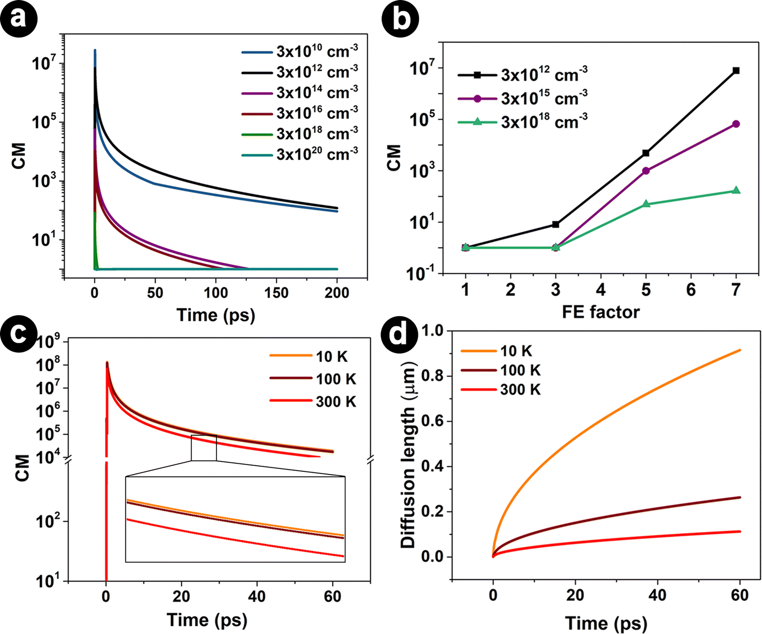 | ||
| Fig. 1 (a) Time dependence of the carrier multiplication as calculated with the diffusive IMI model. (b) CM at t = 1 ps as a function of the FE factor for different initial carrier concentrations. Panels (c) and (d) show the time evolution of CM and the diffusion length as calculated with the diffusive IMI model at FE = 7 for different sample temperatures. | ||
The IMI shows that low dopant concentration is favorable for achieving high carrier multiplication (CM), due to multiple interrelated phenomena. At elevated carrier densities, screening effects become prominent, wherein mobile charge carriers collectively diminish local electric fields induced by plasmonic resonance. Besides, higher carrier densities signify carrier-carrier scattering, resulting in rapid energy dissipation and reduced carrier energy gain.36 Consequently, fewer carriers achieve the necessary kinetic energy to initiate subsequent ionization events.
In intrinsic silicon, with a carrier concentration of approximately 3 × 1010 cm−3, the carrier density increases by seven orders of magnitude within one picosecond due to impact ionization. Under these conditions, on average, only a single electron donor is present in the high-field region around each antenna. This implies that field screening is minimal. At the slightly higher initial carrier concentration of 3 × 1012 cm−3, field screening by free carriers has some influence on the local electric field inside the silicon substrate. Together with carrier scattering, these processes, which in turn reduce the IMI coefficient, weaken the impact ionization process and the CM factor. If n0 is further increased (3 × 1016 cm−3 and 3 × 1018 cm−3 in Fig. 1(a)), the CM factor drops significantly. This trend in CM behavior aligns with the dependence of the IMI coefficient on initial carrier concentration, as reported in Tarekegne's works.35,37 The CM is close to 1 for even higher dopant concentration, i.e., at 3 × 1020 cm−3.
A related insight is obtained from Fig. 1(b), which provides the carrier multiplication factor as a function of the FE factor at t = 1 ps. For n0 > 3 × 1012 cm−3, there is no significant change in carrier concentration if FE ≤ 3. For this reason, we focus on the affected regions with FE > 3 in the following.
Fig. 1(c) and (d) illustrate the temperature dependence of the evolution of the carrier multiplication and diffusion length as predicted by the diffusive IMI model for FE = 7. It can be inferred that a higher temperature leads to a lower carrier multiplication factor and a shorter diffusion length. This dependence arises from the temperature dependence of the diffusion rate D(T), i.e., directly through T in eqn (5), but also through the temperature dependence of the electron and hole mobility. Low temperatures could lead to lower kinetic energy dissipation and lower carrier-phonon scattering. Those insights from the diffusive impact ionization model will be used to interpret the experimental results.
3.2. Static transmission study
Fig. 2(a) shows the false-colored SEM images of metasurface samples MS1, MS2, and MS3. The antenna sizes (1 × 4 μm2) and the Si dopant concentration (2.9 × 1012 cm−3) are the same in those samples, while the x-axis and y-axis periodicities vary from 7.5 × 4.5 μm2, over 7 × 4 μm2, to 6 × 3.5 μm2 for samples MS1, MS2, and MS3, respectively. These unit cell sizes were chosen to evolve from a sample with uncoupled antenna resonances (MS1) to a coupled regime (MS3). As shown in Fig. 2(b), the transmission minimum shifts towards the shorter wavelength (from 24.7 μm over 23.4 μm to 20.7 μm) by decreasing the unit cell size due to the well-known behavior of dipole antennas.38 The wavelength-dependent simulated FE factor at the tip of the antennas and the electric field distribution in the x–y plane at the interface between the antenna and the dielectric substrate for a resonant incoming electromagnetic wave are shown in Fig. 2(c) and (d), respectively. With decreasing unit cell size, there is a stronger coupling between the neighboring antennas, which reduces the quality of dipole resonance, represented by the maximal FE factor and the sharpness of the field enhancement curve close to the resonance. As can be noted, the transmission minimum differs slightly from the wavelength for which the FE factor is maximal. The reason for this is that the field enhancement corresponds to the radiative signal of the antennas, while the transmission dip depends both on the local field confinement and the amount of reflected light. | ||
| Fig. 2 (a) False-colored SEM images of the prepared metasurfaces with different periodicity. The sizes of the golden antennas are the same (4 μm × 1 μm) for the three metasurfaces. (b) Measured FTIR transmission spectra of the three metasurfaces. (c) Simulated spectral dependence of the FE factor at the middle of the longitudinal edge of the antenna for the different metasurfaces (point indicated with the white asterisk in (d)). (d) Simulated electric field distribution at the resonance wavelengths in a single unit cell of the different metasurfaces. The color scale shows the FE factor. | ||
3.3. Dynamic transmission study
To shed more light on the dynamics of the hot carriers, time-resolved pump–probe spectroscopy was used to investigate the effect of pertinent factors such as the substrate's initial carrier concentration, the antennas' dimensions, and the sample's initial temperature. The measurements are compared with simulations based on the diffusive IMI model. | ||
| Fig. 3 Measured (a) and simulated (b) ΔTre (%) of MS2 as a function of pump–probe delay time for different temperatures (10 K, 100 K, and 300 K) at λ = 22.8 μm. Measured (c) and simulated (d) maximal transient change amplitude (ΔTmax/Tt=0) at different temperatures. | ||
Fig. 3(a) presents the transmission after pump excitation of sample MS2 at 22.8 μm for three sample temperatures (300 K, 100 K, and 10 K). The relative transient transmission change is defined as ΔTre (%) = 100(T(t) − T0)/T0 where T(t) is the transmission of the probe beam that is delayed by a time t with respect to the pump, and T0 is the transmittance of the probe if no pump is present. ΔTre is found to be larger at a lower sample temperature, i.e., 7% at 10 K compared to 3.5% at 300 K. In addition, the temperature significantly affects the relaxation process; the relaxation time τre is found to be 80 ps at 10 K and 100 K, and 125 ps at 300 K (procedure to extract the relaxation time is described in the ESI†). Fig. 3(b) presents the corresponding modelled transient transmission change. The temperature-dependent trends are consistent with the experiments. The experimental and measured wavelength dependence of the relative transmission change is presented in Fig. 3(c and d). Here, the maximal transmission change is shown, which typically occurs a few picoseconds after the pump excitation. It is found that cooling the samples from 300 K to 10 K results in a higher transmission increase at wavelengths shorter than the metasurface's resonance and a higher transmission decrease at long wavelengths. This can be attributed to a higher CM factor and longer diffusion length at low temperatures, as predicted by the diffusive IMI model (Fig. 1). Although the first term of eqn (5), which provides the diffusion coefficient, is proportional to the sample temperature, the carrier mobilities decrease at a faster rate with increasing temperature. As a result, the diffusion coefficient and the IMI rate decrease with increasing temperature. This is consistent with prior IMI experimental results and theoretical predictions for the IMI rate.
At low temperatures, there is a reduced kinetic energy dissipation from carrier-phonon scattering; meanwhile, the higher carrier mobility facilitates the acceleration of carriers under the local electric field. Thus, the carrier generation at 10 K is more efficient than at room temperature, resulting in larger ΔTre. Besides, the carrier lifetime is shorter at low temperatures due to a higher probability of the recombination processes, which explains the observed faster decay. Those trends are consistent in experimental and modeled results and can be attributed to the inclusion of a temperature-dependent carrier diffusion coefficient in our model.
Comparing the values in Fig. 3(b) with those in Fig. 3(a) and (d) with those of Fig. 3(c), it can be seen that the absolute values of the modeled ΔTre are higher than the measured values. This can be attributed to the difference in the static transmission minimum at resonance, which is 0.1 in the experiment and 0.06 in the simulation (will be discussed on the basis of Fig. 5).
 | ||
| Fig. 4 The transient transmission change of samples MS1 (black), MS2 (red), and MS3 (blue), measured at 22.8 μm (a), 26.2 μm (b), and 34 μm (c). | ||
Fig. 5(a) presents the measured transmission spectra of MS1 for a fixed pump–probe delay of 15 ps and compares them with the spectrum obtained without a pump laser. Under pump pulse influence, the transmission minimum shifts slightly to the longer wavelength, and the spectrum becomes flatter. The simulation in Fig. 5(b) reproduces those changes well. The spectral changes can be understood as follows. Free carriers generated by IMI due to the local field enhancement around the tips of the antennas (Fig. 2(d)) spread out to the surrounding silicon space, causing the change of carrier concentration both in time and space. Such change leads to the spectral shift of the resonance wavelength. Furthermore, the plasmonic resonance considerably broadens after laser excitation, owing to a strong increase in the silicon substrate carrier concentration, causing a rise in the Ohmic losses. In this regard, by combining the diffusive IMI model and FDTD simulation, we could effectively capture both effects (spectral shift and peak broadening) using the Drude model for silicon.39 Similar to the temperature dependence investigation (Fig. 3), the simulation's absolute value for the transmission change is larger. The transmission of the MSs on the blue side of plasmonic resonance increases, and at the same time, transmission reduction is observed on the red side. On the other hand, MS2 and M3 display significantly less peak broadening, a smaller transmission change, and minimal spectral shifts (see simulation in ESI† Fig. S5). Those differences for different sample geometries can be related to the higher field enhancement of MS1, which has uncoupled antennas.
 | ||
| Fig. 5 Panel (a) and (b) show the experimental and simulated transmittance of MS1 without a pump and for a pump–probe delay of 15 ps. | ||
Transient transmission change maps based on the excitation wavelength and pump–probe delay reveal the wavelength-dependent dynamic response of the metasurfaces more clearly. According to the data obtained in Fig. 6, different dynamics can be achieved depending on the relative positions of the pump–probe wavelength and the plasmonic resonance. In the case of MS1, there is an increase in transmission for excitation at the center or shorter wavelengths of the resonance and a decrease in transmission for the longer wavelengths. In sample MS2, a mixed behavior is observed in a narrow wavelength range between those two regions (i.e., in the 24–26 μm range). The transient transmission changes for MS3 are qualitatively similar to MS1 but have a lower intensity. In general, sample MS1 exhibits the strongest response, which can be attributed to its highest FE factor.
 | ||
| Fig. 6 Transient transmission change ΔTre of different metasurfaces – MS1 (a), MS2 (b), MS3 (c), and MS4 (d) – as a function of the pump–probe delay and the FIR wavelength. The horizontal dashed line indicates the plasmonic resonance of the different metasurfaces. The resonance for MS3 (panel c) is not shown because it is out of the range of the figure. | ||
Lastly, we investigate the influence of the initial dopant concentration in the silicon substrate on the dynamics. Sample MS4 was fabricated with the same geometry as MS1 but has a higher silicon dopant concentration of 1.6 × 1015 cm−3 (compared to 2.9 × 1012 cm−3 in MS1). The higher initial carrier concentration causes more carrier scattering events and a more substantial electric field screening effect, significantly reducing the kinetic energy of carriers with as result that they do not contribute to the impact ionization. This explains the modest transient transmission change in MS4 (Fig. 6(d)). This conclusion is in line with related studies regarding the surface recombination of electron–hole pairs generated by IMI indirect band gap semiconductors.40 A low initial carrier concentration (as in MS1) is important to ensure a strong dynamic response. Those results demonstrate how changes in the metasurface geometry and the initial carrier concentration can be used to engineer the dynamic optical response.
4. Conclusions
The findings of this study provide a better knowledge of plasmonic-induced impact ionization in silicon and the subsequent relaxation. The influences of the metasurface geometry, the initial carrier concentration of the silicon substrate, and the sample temperature on carrier dynamics were investigated. The obtained results revealed that the transient transmittance change depends on the pump–probe laser's relative position compared to the metasurface's plasmon resonance. If the pump–probe laser excites the metasurfaces close to their plasmonic resonance, transmittance changes of up to 60% could be achieved. It was inferred that changing the antenna coupling through the periodicity of the metasurface shifted the transmission minimum towards shorter wavelengths and affected the field enhancement significantly. Increasing the temperature adversely affected the IMI rate, charge multiplication factor, and diffusion length. Lastly, a low initial dopant concentration was found to be favorable for achieving a maximal dynamic response. The simulations from the proposed diffusive IMI model validated the experimentally obtained results and provided further insight into the underlying carrier dynamics. This increased understanding of the dynamics of metasurfaces can be used to improve energy harvesting systems as active elements in FIR image cameras and simple optical nonlinear high-frequency switches. Building on the findings of this work, the impact ionization effect can be effectively utilized to induce ultrafast optical modulation in metasurfaces, positioning it as a promising mechanism for next-generation ultrafast photonic devices. However, further advancements towards obtaining higher quality factors and lower radiative losses are needed.Conflicts of interest
There are no conflicts of interest to declare.Data availability
The experimental data, the simulation results, and the computer code of the theoretical model (diffusive impact ionization model) supporting this article are included in the manuscript and the ESI.†Acknowledgements
This work has been supported by a joint research project between the Research Foundation Flanders (FWO) under Grant G0DAX23N and the Vietnam National Foundation for Science and Technology Development (NAFOSTED) under Grant No. FWO.103-2022.01. T. L. P. acknowledges the KU Leuven Research Council for IRO scholarhsip ZB/21/023. The authors acknowledge support of CALIPSOplus project under HORIZON 2020 GA730872 from the EU Framework Program for Research and Innovation; they thank the FELIX staff and are grateful to the Nederlandse Organisatie voor Wetenschappelijk Onderzoek (NWO) for the support of the FELIX Laboratory.References
- L. Zhou, Q. Huang and Y. Xia, Chem. Rev., 2024, 124, 8597–8619 CrossRef CAS PubMed.
- Y. Park, I. Hamada, A. Hammud, T. Kumagai, M. Wolf and A. Shiotari, Nat. Commun., 2024, 15, 6709 CrossRef CAS PubMed.
- A. Stefancu, N. J. Halas, P. Nordlander and E. Cortes, Nat. Phys., 2024, 20, 1065–1077 Search PubMed.
- L. Zhang, X. Wang, Z. Zheng, C. Zhang, H. Zheng, C. Liu, H. Chen and M. Wang, Nano Lett., 2024, 24, 11654–11660 CrossRef CAS PubMed.
- M. Hong, R. B. Dawkins, B. Bertoni, C. You and O. S. Magaña-Loaiza, Nat. Phys., 2024, 20, 830–835 Search PubMed.
- C. Zhang, H. Hu, C. Ma, Y. Li, X. Wang, D. Li, A. Movsesyan, Z. Wang, A. Govorov, Q. Gan and T. Ding, Nat. Commun., 2024, 15, 2 Search PubMed.
- H. Zhou, D. Li, Z. Ren, C. Xu, L. F. Wang and C. Lee, Sci. Adv., 2024, 10, eado3179 Search PubMed.
- C. Jung, E. Lee and J. Rho, Sci. Adv., 2024, 10, eado8964 Search PubMed.
- F. Han, T. L. Pham, K. Pilarczyk, N. T. Tung, D. H. Le, G. A. E. Vandenbosch, J. Van de Vondel, N. Verellen, X. Zheng and E. Janssens, Adv. Opt. Mater., 2024, 12, 2303085 Search PubMed.
- A. Jain, H. Northfield, E. Karimi, P. Berini and R. Bhardwaj, ACS Nano, 2024, 18, 27383–27392 CrossRef CAS PubMed.
- Y. Lai, D. D. A. Clarke, P. Grimm, A. Devi, D. Wigger, T. Helbig, T. Hofmann, R. Thomale, J. S. Huang, B. Hecht and O. Hess, Nat. Commun., 2024, 15, 6324 CrossRef CAS PubMed.
- K. S. Sunil and J.-S. Huang, ACS Appl. Opt. Mater., 2025, 3, 483–493 CrossRef CAS.
- A. T. M. Yesilyurt, X. Wu, K. Tapio, I. Bald and J. S. Huang, J. Am. Chem. Soc., 2023, 145, 25928–25932 CrossRef CAS PubMed.
- C. O. Karaman, A. Y. Bykov, F. Kiani, G. Tagliabue and A. V. Zayats, Nat. Commun., 2024, 15, 703 CrossRef CAS PubMed.
- A. Amirjani, N. B. Amlashi and Z. S. Ahmadiani, ACS Appl. Nano Mater., 2023, 6, 9085–9123 CrossRef CAS.
- A. Amirjani, P. Shokrani, S. A. Sharif, H. Moheb, H. Ahmadi, Z. S. Ahmadiani and M. S. Paroushi, J. Mater. Chem. B, 2023, 11, 3537–3566 RSC.
- A. Amirjani, T. V. Tsoulos, S. H. Sajjadi, A. Antonucci, S.-J. Wu, G. Tagliabue, D. F. Haghshenas and A. A. Boghossian, Carbon, 2022, 194, 162–175 CrossRef CAS.
- V. Coviello, D. Badocco, P. Pastore, M. Fracchia, P. Ghigna, A. Martucci, D. Forrer and V. Amendola, Nat. Commun., 2024, 15, 834 CrossRef CAS PubMed.
- V. Coviello, D. Forrer and V. Amendola, Chem. Phys. Chem., 2022, 23, e202200136 CrossRef CAS PubMed.
- J. L. Yang, H. J. Wang, X. Qi, Q. N. Zheng, J. H. Tian, H. Zhang and J. F. Li, ACS Appl. Mater. Interfaces, 2024, 16, 12149–12160 CrossRef CAS PubMed.
- S. Inoue, T. Yokoyama, K. Sasaki, H. Misawa and H. Ishihara, J. Phys. Chem. C, 2024, 128, 2796–2802 CrossRef CAS.
- A. J. Bagnall, S. Ganguli and A. Sekretareva, Angew. Chem., Int. Ed., 2024, 63, e202314352 CrossRef CAS PubMed.
- L. Xu, J. He, W. Tang, C. Yang, L. Han, L. Zhang, H. Zhu, S. Liu, C. Liu, M. Qiu, G. Li and X. Chen, Laser Photonics Rev., 2023, 18, 2300643 CrossRef.
- M. Maiuri, A. Schirato, G. Cerullo and G. Della Valle, ACS Photonics, 2024, 11, 2888–2905 CrossRef CAS.
- M. Bejide, Y. Li, N. Stavrias, B. Redlich, T. Tanaka, V. D. Lam, N. T. Tung and E. Janssens, Opt. Express, 2021, 29, 170–181 CrossRef CAS PubMed.
- E. Cartier, M. V. Fischetti, E. A. Eklund and F. R. McFeely, Appl. Phys. Lett., 1993, 62, 3339–3341 CrossRef CAS.
- D. Oepts, A. F. G. van der Meer and P. W. van Amersfoort, Infrared Phys. Technol., 1995, 36, 297–308 CrossRef CAS.
- N. Q. Vinh, B. Redlich, A. F. G. van der Meer, C. R. Pidgeon, P. T. Greenland, S. A. Lynch, G. Aeppli and B. N. Murdin, Phys. Rev. X, 2013, 3, 011019 Search PubMed.
- A. Irizawa, S. Suga, T. Nagashima, A. Higashiya, M. Hashida and S. Sakabe, Appl. Phys. Lett., 2017, 111, 26093–26102 CrossRef.
- J. Zhang, X. Zhao, K. Fan, X. Wang, G.-F. Zhang, K. Geng, X. Zhang and R. D. Averitt, Appl. Phys. Lett., 2015, 107, 231101 CrossRef.
- A. V. Ovchinnikov, O. V. Chefonov, M. B. Agranat, A. V. Kudryavtsev, E. D. Mishina and A. A. Yurkevich, Opt. Express, 2021, 29, 26093–26102 CrossRef CAS PubMed.
- H. Wen, M. Wiczer and A. M. Lindenberg, Phys. Rev. B: Condens. Matter Mater. Phys., 2008, 78, 125203 CrossRef.
- Y. Yang, Y. Yan, M. Yang, S. Choi, K. Zhu, J. M. Luther and M. C. Beard, Nat. Commun., 2015, 6, 7961 CrossRef CAS PubMed.
- C. Jacoboni, C. Canali, G. Ottaviani and A. Alberigi Quaranta, Solid State Electron., 1977, 20, 77–89 CrossRef.
- A. T. Tarekegne, K. Iwaszczuk, M. Zalkovskij, A. C. Strikwerda and P. U. Jepsen, New J. Phys., 2015, 17, 043002 CrossRef.
- F. Meng, M. D. Thomson, B. E. Sernelius, M. Jörger and H. G. Roskos, Phys. Rev. B: Condens. Matter Mater. Phys., 2015, 91, 075201 CrossRef.
- A. T. Tarekegne, H. Hirori, K. Tanaka, K. Iwaszczuk and P. U. Jepsen, New J. Phys., 2017, 19, 123018 CrossRef.
- H. Wakatsuchi, J. Paul, S. Greedy and C. Christopoulos, IEEE Trans. Antennas Propag., 2012, 60, 3670–3678 Search PubMed.
- K. J. Willis, S. C. Hagness and I. Knezevic, Appl. Phys. Lett., 2013, 102, 122113 CrossRef.
- E. Najafi and A. Jafari, J. Appl. Phys., 2019, 125, 185303 CrossRef.
Footnotes |
| † Electronic supplementary information (ESI) available. See DOI: https://doi.org/10.1039/d5ma00127g |
| ‡ These authors contributed equally. |
| This journal is © The Royal Society of Chemistry 2025 |