
 Open Access Article
 This Open Access Article is licensed under a Creative Commons Attribution-Non Commercial 3.0 Unported Licence
van der Waals epitaxial growth of hexagonal boron nitride on graphene for enhanced deep ultraviolet sensing performance†
Hoang Hung
Nguyen
a,
Seongjun
Kim
b,
Tran Viet
Cuong
a,
Huynh Tran My
Hoa
a,
Anh Hao Huynh
Vo
a,
Thien Trang
Nguyen
a,
Kang Bok
Ko
c and
Young Jae
Park
 *b
*b
aVKTech Research Center, NTT Hi-Tech Institute, Nguyen Tat Thanh University, 298-300A Nguyen Tat Thanh Street, District 4, Ho Chi Minh City, Vietnam
bNational Institute for Nanomaterials Technology, Pohang University of Science and Technology, Cheongam-Ro 77, 37673 Pohang, Republic of Korea. E-mail: youngjaepark@postech.ac.kr
cSchool of Semiconductor and Chemical Engineering, Jeonbuk National University, Jeonju 54896, Republic of Korea
First published on 28th June 2025
Abstract
The integration of hexagonal boron nitride (h-BN) and graphene, known as a van der Waals heterostructure (vdWHT), holds significant potential as a fundamental platform for developing innovative two-dimensional devices such as ultra-thin transistors, capacitors, and photodetectors. However, the currently employed fabrication methods often involve mechanical assembly, which can introduce defects and limit scalability. Herein, we demonstrate a scalable approach to grow lattice-matched h-BN on graphene via metal–organic chemical vapor deposition with a flowrate-modulated epitaxy method. TEM analysis revealed the successful growth of 7 to 8 layers of h-BN on the substrates. Notably, vdWHT h-BN/graphene exhibited superior optical and structural properties compared with h-BN/sapphire. This was evident in the results of UV-Vis and Raman spectroscopies and SEM analysis. Moreover, vdwHT h-BN/graphene demonstrated significantly enhanced DUV sensing performance at 254 nm, with an excellent on/off ratio exceeding 110 compared with the ratio of 3.8 of h-BN/sapphire. These findings underscore the importance of lattice matching in optimizing the properties of h-BN-based heterostructures. The successful fabrication of high-quality vdwHT h-BN/graphene heterostructures opens a new avenue for the development of advanced DUV sensing devices and other 2D applications.
1. Introduction
Hexagonal boron nitride (h-BN), often referred to as ‘white graphene’, is a two-dimensional material with a graphene-like honeycomb structure, featuring tightly bonded sp2-hybridized BN atoms. Among the BN allotropes, h-BN's exceptional mechanical durability, thermal conductivity, and chemical inertness make it a versatile material for applications in energy conversion,1–3 biomedicine,4–6 environment,7,8 photonics and electronics.9–12 In photoelectronics, h-BN's indirect bandgap of 5.96 eV makes it an ideal candidate for deep ultraviolet (DUV) photonic device applications, as evident from a series of recent publications related to h-BN photoelectronic devices.9,13–17 Recent studies have explored numerous ways to enhance the performance of h-BNs in DUV sensing applications; for instance, Heng Liu et al. demonstrated a high-performance DUV photodetector fabricated using a few-layers of h-BN on SiO2/Si substrates, achieving an on/off ratio exceeding 1000 under an irradiation of 212 nm.18 The modified h-BN also improved the DUV sensing performance; Wang et al. investigated the effects of carbon doping on h-BN's DUV sensing performance, revealing that a 7.5% carbon doping ratio was optimal for improving the sensitivity.17Owing to its similar in-plane lattice constant to graphene, h-BN is a promising material for vdWHTs. These heterostructures offer new possibilities for developing innovative 2D devices.19–25 However, the wafer-scale growth of h-BN remains a significant challenge owing to the difficulties in controlling uniformity and thickness at a large scale.26 Among the h-BN synthesis methods, metal–organic chemical vapor deposition (MOCVD) has been proposed (Top Engineering, model: Phaethon 100U, asset ID: NFEC-2013-04-177491, located at the Semiconductor Process Research Center, SPRC) as a highly promising solution to achieve wafer-scale growth of 2D materials on sapphire or other substrates. For growing h-BN with high crystalline quality, high temperature is necessary to promote the surface migration of B atoms and B-free radicals. However, an increase in temperature generates gas-phase prereactions among the precursors, leading to adduct formation—commonly referred to as a parasitic reaction. This issue can be mitigated by employing an alternative precursor supply method, such as sequential or pulsed injection, which prevents simultaneous precursor mixing in the gas phase, as reported in previous studies.27,28 This approach not only suppresses parasitic reactions but also enhances adatoms migration across the substrate surface. However, optimizing the flow rates of both the precursors can be challenging as it significantly influences the growth rate and V/III flux ratios, in principle.29–31
Herein, a vdWHT of h-BN and graphene was fabricated, in which h-BN was synthesized on a 2-inch transferred graphene/sapphire wafer via an MOCVD method. It was then used to investigate the DUV sensing performance at an excitation wavelength of 254 nm. Another photodetector made from h-BN grown directly on sapphire was used as the controlled device. Results demonstrated that the h-BN/graphene/sapphire photodetector exhibited significantly superior properties, highlighting the advantages of this vdWHT structure in DUV sensing performance.
2. Experimental
2.1. Growth of h-BN epilayers
A two-dimensional heterojunction between h-BN and graphene was successfully fabricated on sapphire substrates via a combined temperature-step and pulse-flow growth method. The h-BN layers were epitaxially grown via MOCVD on either a 2-inch CVD-grown graphene layer that was transferred onto a substrate, or on a sapphire wafer (both provided by Hanwha Aerospace Company). A reference sample consisting of h-BN grown directly on a 2-inch sapphire wafer (Hanwha Aerospace Company) was also prepared. The vertical MOCVD reactor operated at 30 torr, with triethyl boron (TEB) and ammonia (NH3) as precursors for boron (B) and nitrogen (N) sources, respectively, with hydrogen (H2) as the carrier gas.Fig. 1a shows three stages of temperature sequence for h-BN epitaxy process. Prior to h-BN growth, the thermal treatment process was carried out by annealing in ambient nitrogen gas (N2) at 1100 °C for 3 minutes, which was found to be critical for h-BN growth.32 After thermal treatment, further h-BN epilayer growth was carried out by introducing the precursor while using a step-grown temperature approach, which involves the growth h-BN layers at a low temperature (LT) followed by a high temperature (HT) via a flowrate-modulated epitaxy (FME) technique. The timing of the FME technique is shown in Fig. 1b, which includes the injection of 2.9 μmol min−1 of TEB for 4 seconds before the injection of 1000 sccm of NH3 for 4 seconds while continuously injecting the H2 carrier. The precursor gas flow was interrupted for 2 seconds between the injection of B and N sources, creating a modulated gas flow cycle of 12 second. This FME technique helped to avoid nitrogen migration and suppressed the occurrence of the gas-phase parasitic reaction. The LT h-BN layer was grown at 800 °C for over 12 cycles in 5 minutes to form a buffer layer, which was essential for a flat- and defect-free surface for subsequent growth. At LT, the slower decomposition of precursors led to a slower growth rate and a smoother film, reducing the influence of thermal expansion from the substrate during epitaxy. Additionally, the LT buffer layer enhanced the connectivity of the h-BN epilayer on the substrates.33 Previous studies have demonstrated that buffer layers are effective for h-BN growth on sapphire substrates, primarily to mitigate lattice mismatch. However, the necessity of a buffer layer for h-BN growth on graphene/sapphire is not well established. Despite the similar lattice constants of graphene and h-BN, the role of a buffer layer in this system remains unclear.
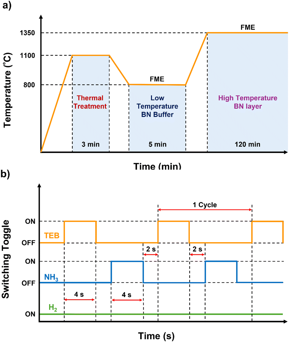 | ||
| Fig. 1 Schematic illustration of the h-BN growth sequence using a stepwise temperature profile and flow-modulated epitaxy (FME) process. (a) Step-temperature growth sequence comprising thermal treatment (∼1100 °C, 3 min), low-temperature BN buffer growth (∼800 °C, 5 min), and high-temperature BN layer deposition (∼1350 °C, 120 min), with FME applied during BN growth stages. (b) Timing diagram for one FME cycle, showing sequential pulsing of triethylboron (TEB, 4 s ON), ammonia (NH3, 4 s ON), and hydrogen (H2, continuous), repeated for each growth cycle. | ||
In our study, a low-temperature buffer layer was used based on standard protocols for sapphire substrates. However, we did not directly compare growth with and without the buffer layer on graphene/sapphire owing to experimental constraints in this study. The susceptor temperature was increased to 1350 °C to initiate the HT process, thus growing the primary epitaxial h-BN layers at 180 FME cycles in 120 minutes. Neither the low-temperature buffer layer process nor the FME technique was confirmed to be essential for the synthesis method used in this study. While these techniques were employed in the process, no direct control experiments were conducted to confirm their necessity. Thus, these results do not confirm the absolute requirements of these methods, and further investigation in future studies may explore their impact on the synthesis process.
The morphologies of h-BN/graphene/sapphire and h-BN/sapphire interfaces were investigated using SEM and high-resolution TEM (HRTEM) analyses. UV-Vis and Raman spectroscopies (using a 532-nm Nd:YAG laser with E2g Raman mode) were applied to characterize the optical properties of the grown h-BN films.
2.2. Fabrication and characterization of the DUV photodetector
Based on our previous work to grow an h-BN film on graphene, we successfully implemented an h-BN/graphene heterostructure and fabricated the photodetector device, operating at deep UV region. Fig. 2 depicts the structure of the h-BN/graphene/sapphire photodetector with an Ni/Au layer acting as the conducting electrode. The fabricated devices possessed the dimensions of 0.4 × 0.8 cm2 and a photoactive area of 64 × 10−5 cm2. The photoresponse of the fabricated h-BN/graphene/sapphire photodetector was characterized by monitoring the current–voltage change (Keithley 4200-MStech) under a 254-nm light irradiation. Another photodetector device obtained from an h-BN film grown on sapphire was tested for the purpose of comparison. A xenon lamp (450 W) and an Oriel Cornerstone 130 1/8m monochromator were used as light sources to record the responsivity spectrum.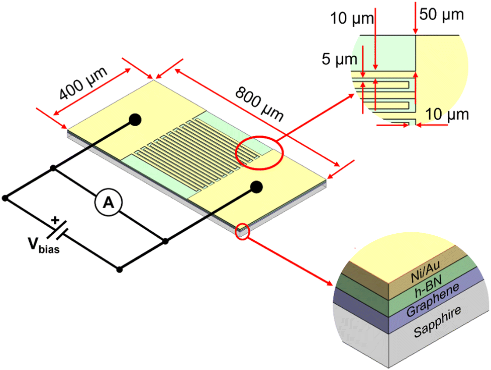 | ||
| Fig. 2 Schematic of the fabricated photodetector using h-BN grown on graphene with an Ni/Au electrode layer for DUV detection. | ||
3. Results and discussion
The nucleation and growth of h-BN epilayers on substrate surfaces using the MOCVD technique proceed through a highly complex, multi-step formation pathway, influenced by various surface reactions and precursor dynamics. Fig. 3 illustrates the mechanism of h-BN formation from the precursors TEB and NH3 during the MOCVD growth process. The initial step involved the pyrolysis of the TEB precursor, resulting in the formation of B-based compounds. Under high-temperature conditions, TEB decomposed into borane compounds by cleaving the ethyl radical groups (C2H5*), which were subsequently converted into more stable compounds, including C2H4, C4H10, and H2. Prior to the introduction of NH3, these borane compounds combined to form diborane, which was characterized by two bridging hydrogen elements (B–H–B) due to three-center two-electron bonding.34,35 The thermal decomposition process was continued until the formation of boron monohydride (BH), which subsequently decomposed into B adatoms on the substrate. When NH3 was introduced into the reaction chamber, it reacted with the B adatoms, which created the B–N bonds on the substrate,36 initiating the h-BN nucleation in MOCVD. During the growth process, owing to the Lewis acid property of borane compounds, they were able to share an electron couple with NH3, forming amine borane compounds. These compounds interacted with each other to form borazine compounds, exhibiting a benzene-like ring structure. Similarly, diborane compounds reacted with NH3 to form borazine compounds.37 These compounds featured B–N bonds and contained B–H or B–C2H5 bonds, depending on the specific borane compound involved. The decomposition of borazine compounds produced small BN molecules that linked together to form h-BN. | ||
| Fig. 3 Transformation pathways of precursors into h-BN during MOCVD. | ||
Fig. 4 presents the optical properties of h-BN layers synthesized on graphene and sapphire substrates via the MOCVD method. The Raman spectra with Gaussian fitting curves are shown in Fig. 4a, in which the distinctive feature indicating sp2-hybridized BN is the E2g mode. This mode originated from the vibrations of boron and nitrogen, moving in opposite directions within the plane of the h-BN lattice.38–40 The h-BN grown on graphene revealed a characteristic E2g mode peak at approximately 1364 cm−1, which was consistent with previous reports.26,40,41 In this study, the graphene/sapphire Raman spectrum, including the D-peak, is shown in Supplementary information S1 (ESI†) and was used for reference, but it was not subtracted in the presented spectrum in Fig. 4(a). The D-peak, which is a characteristic of defects in graphene, could overlap with the E2g peak of h-BN, potentially affecting the estimation of the E2g FWHM. We acknowledge that this overlap could influence the FWHM calculation; however, for the analysis in Fig. 4(a), the D-peak was not removed from the spectrum. The FWHM of the E2g peak for vdWHT h-BN/graphene/sapphire was 16.2 cm−1, which was narrower than that for h-BN/sapphire (23.8 cm−1). Additionally, a small red shift was observed for h-BN/sapphire (wavenumber peak at 1362 cm−1) compared with vdWHT h-BN/graphene/sapphire. Previous studies have reported that the red shift in the Raman spectra of h-BN layers is correlated with both the thickness26 and tensile strain42 of the layers. This indicates that the higher tensile strain in h-BN layers on sapphire may result from the lower structural stability of the sapphire surface compared to the graphene/sapphire substrate. Although no direct evidence was observed in the samples for significant carbon contamination, the possibility of low levels of carbon contamination cannot be completely excluded, particularly because of the TEB decomposition process. The UV-Vis spectra with an inset of Tauc plots are shown in Fig. 4b. Both vdWHT h-BN/graphene/sapphire and h-BN/sapphire exhibited significant increase in photon absorption at 200 nm. Tauc plot analysis yielded bandgap values of 5.96 eV and 5.88 eV for vdWHT h-BN/graphene/sapphire and h-BN/sapphire, respectively. While the obtained bandgap value of vdWHT h-BN/graphene/sapphire aligned well with the reported indirect bandgap of h-BN,43 the bandgap of h-BN/sapphire was slightly lower. These optical properties indicated a higher degree of crystallinity and fewer defects in h-BN epilayers grown on graphene compared with those grown on sapphire.
 | ||
| Fig. 4 Raman spectrum of h-BN grown on sapphire and on graphene (a) and UV-Vis absorption spectrum of h-BN grown on sapphire (black line) and graphene (red line); inset: Tauc plot for bandgap identification (b). | ||
The morphology of the h-BN epitaxial layers, grown on both graphene/sapphire and sapphire substrates, were examined using SEM and AFM techniques. The SEM image depicting the h-BN growth on graphene (Fig. 5a) revealed a notably smooth surface morphology. In contrast, the surface of h-BN grown on sapphire (Fig. 5b) displayed numerous grain formations and wrinkle patterns. These morphological differences could be attributed to the lattice mismatch between the h-BN epilayers and substrates. As previously reported,44,45 the in-plane lattice constant of h-BN is approximately 2.496 ± 0.006 Å in the temperature range of 500 °C to 1500 °C. This value closely matches the in-plane lattice constant of graphene on sapphire, which is 2.44 ± 0.02 Å,46 resulting in a lattice mismatch of around 2.2% for vdWHT h-BN/graphene. In comparison, the in-plane lattice constant of sapphire is 4.78 ± 0.015 Å in the temperature range of 500 °C to 1200 °C, leading to a significantly larger lattice mismatch between h-BN and sapphire. This substantial mismatch explained the presence of rough grains and wrinkles on h-BN/sapphire. The measured surface roughness (RMS) values from the AFM images of h-BN epilayers grown on sapphire substrates with graphene (Fig. 5c) and without graphene (Fig. 5d) were 0.826 nm and 0.914 nm, respectively. The surface roughness was regarded as ESI,† for the explanation of the SEM data. These results implied that smoother morphology and fewer defects observed in vdWHT h-BN/graphene/sapphire correlate with its improved optical properties, as discussed previously.
 | ||
| Fig. 5 SEM (a) and (b) and AFM images (c) and (d) of vdWHT h-BN/graphene/sapphire and h-BN/sapphire, respectively. | ||
Fig. 6 displays the cross-sectional HRTEM images of vdWHT h-BN/graphene/sapphire and h-BN/sapphire along the11,20 zone axis, with supplementary electron diffraction patterns. Two distinct layers with different structures were observed in h-BN grown on sapphire (Fig. 6a). The upper layer, which was closer to the surface, was a well-oriented layer consisting of a stack of h-BN epilayers in highly ordered basal planes. This stack included 7 to 8 h-BN multilayers intact on the sapphire substrate, with a layer thickness of approximately 0.33 nm, as determined from the line profile provided in the inset. Fig. 6b shows three distinct layers from the top-down view, belonging to h-BN epilayers, graphene, and sapphire. This observation was further confirmed using electron diffraction patterns.
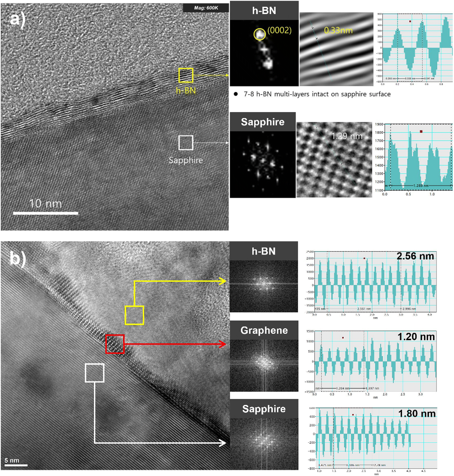 | ||
| Fig. 6 Cross-sectional high-resolution transmission electron microscopy (HRTEM) images and corresponding structural analyses of (a) h-BN/sapphire and (b) van der Waals heterostructure (vdWHT) h-BN/graphene/sapphire samples. In (a), 7–8 layers of h-BN are observed directly grown on the sapphire substrate, with clear (0002) lattice fringes (∼0.33 nm spacing) indicating good crystallinity. The inset shows an enlarged view of the h-BN lattice, FFT pattern, and corresponding intensity profile, confirming uniform interlayer spacing and structural coherence with the sapphire interface. In (b), the vdWHT sample shows sequentially stacked h-BN (∼2.56 nm), monolayer graphene (∼1.20 nm), and sapphire. Insets highlight the distinct contrast between layers, FFT patterns for each region, and line profiles indicating their respective periodicities. The presence of the graphene interlayer enhances the structural order of h-BN and reduces interfacial strain compared to direct growth on sapphire. | ||
Fig. 7a presents the photoresponsivity of the vdWHT h-BN/graphene/sapphire photodetector at a bias voltage of −100 V, with an inset showing the top-view of the fabricated device. The responsivity spectrum demonstrates the device's response in the DUV region, which was consistent with the UV-Vis analysis, and exhibited a significant increase with decreasing wavelength. At 200 nm, the responsivity reached a peak of 10.335 mA W−1, while the responsivity in the non-DUV region was below 1.326 mA W−1. This result indicated the high sensitivity of the vdWHT h-BN/graphene/sapphire photodetector to DUV radiation. The I–V curves of vdWHT h-BN/graphene/sapphire and h-BN/sapphire photodetectors with and without a 254-nm irradiation are shown on Fig. 7b. The I–V characteristic of the vdWHT h-BN/graphene/sapphire photodetector exhibited a superior performance compared with h-BN/sapphire. Without irradiation, the dark current density of vdWHT h-BN/graphene/sapphire was 8.91 × 10⁻¹⁰ A cm−2 at −100 V, while the photocurrent density was 1.01 × 10⁻⁷ A cm−2 at −100 V. This resulted in a signal-to-noise ratio of over 110. On the contrary, the h-BN/sapphire photodetector exhibited a dark current density of 6.41 × 10⁻¹⁰ A cm−2 and a photocurrent density of 2.45 × 10⁻⁹ A cm−2 at −100 V, yielding a signal-to-noise ratio of only 3.8.
 | ||
| Fig. 7 (a) Photoresponse spectra of vdWHT h-BN/graphene/sapphire photodetector at a −100-V bias voltage; inset: top-view of the fabricated devices and (b) I–V characteristics of the vdWHT h-BN/graphene/sapphire and h-BN/sapphire photodetectors under a 254-nm light irradiation. | ||
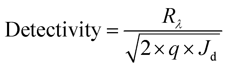
To further investigate the performance of the h-BN-based photodetectors, a comparison of different recently reported photoconductive DUV sensors obtained from this type of material was conducted (Table 1). Detectivity was calculated using the specific detectivity formula provided below:
| Properties | |||||||
|---|---|---|---|---|---|---|---|
| Material | Growth method | Tested wavelength (nm) | Responsivity (A W−1) | Detectivity (Jones) | Photo-to-dark current ratio | Dark current (A) | Active area (cm2) |
| IBD: ion beam deposition; SSR: solid-state reaction; LPD: laser plasma deposition; CVD: chemical vapor deposition. | |||||||
| h-BN/sapphire (this work) | MOCVD | 254 | — | — | 3.8 | 5.7 × 10⁻¹³ | 64 × 10−5 |
| h-BN/graphene/sapphire (This work) | MOCVD | 254 | 4.03 × 10⁻³ | 2.82 × 10¹¹ | 113.3 | 4.1 × 10⁻¹³ | 64 × 10−5 |
| 7.5% carbon-doped h-BN/SiO2/Si17 | IBD | 212 | 9.2 × 10⁻³ | 3.09 × 10¹¹ | — | 43.9 × 10⁻⁹ | — |
| h-BN/SiO2/Si18 | IBD | 212 | 0.1 × 10⁻³ | 2.4 × 10⁸ | 103 | — | 25 × 10−4 |
| Thick film h-BN/Quartz47 | IBD | 204 | 0.5 | 6.92 × 10⁹ | 103 | — | 15 × 10−4 |
| h-BN/Cu48 | SSR | 210 | 5.022 | 6.1 × 10¹² | 100 | — | 1 |
| h-BNNs/Mo49 | LPD | 254 | 1.5 × 10⁻³ | — | 1.5 | 200 × 10−9 | 2 × 10⁻³ |
| BN/Au50 | CVD | 160-400 | 0.7 × 10⁻⁶ | 1.55 × 10⁸ | 115.04 | — | 0.21 |
| h-BN/SiO2/Si51 | CVD | 220 | 0.45 | 2.8 × 10¹⁰ | — | — | — |
| h-BN/SiO2/Si52 | CVD | 220 | 3.4 × 10⁻³ | 3.9 × 10¹⁰ | — | 10−10 | — |
| h-BN/SiO2/Si53 | CVD | 210 | 5.45 × 10⁻³ | 8.62 × 10⁹ | 45 | 9 × 10⁻¹³ | 7 × 10⁻⁵ |
4. Conclusions
This work successfully fabricated a 2-inch vdWHT h-BN/graphene vdWHT via an MOCVD method using the FME technique. HRTEM analysis revealed approximately 7 to 8 layers of h-BN epitaxy on the substrate. Owing to the small lattice mismatch between h-BN and graphene, the vdWHT h-BN/graphene structure exhibited superior properties compared with the h-BN grown on sapphire. UV-Vis spectroscopy demonstrated a higher absorption intensity for vdWHT h-BN/graphene/sapphire than h-BN/sapphire. Additionally, a slight red shift observed in the Raman spectrum of h-BN/sapphire (1362 cm−1) compared with vdWHT h-BN/graphene/sapphire (1364 cm−1) indicated structural defects in h-BN/sapphire. SEM images confirmed the presence of rough grains and wrinkles on h-BN/sapphire, while vdWHT h-BN/graphene exhibited a smoother surface, highlighting it as the perfect buffer of graphene to grow h-BN. The superior structure of vdWHT h-BN/graphene directly influenced its optoelectronic properties in DUV applications. Fewer defects in vdWHT h-BN/graphene led to higher electron mobility, resulting in a significantly higher SNR of 110 compared with the SNR of 3.8 for h-BN/sapphire in DUV sensing performance. This achievement highlights the potential of lattice-matched vdWHT h-BN/graphene for enhancing the performance of DUV sensors and other related applications.Conflicts of interest
There are no conflicts to declare.Data availability
The raw experimental data used in this study are not publicly available owing to confidentiality and data protection regulations. However, data requests can be directed to the corresponding author. All data used in this study are generated during the course of the research and do not include publicly available datasets.Acknowledgements
This work was supported by the National R&D Program through the National Research Foundation of Korea (NRF), funded by the Ministry of Science and ICT (NRF-2022M3H4A1A04074153). Support from the Nguyen Tat Thanh University Research Grant (NTTU-2025) in Vietnam is also gratefully acknowledged.References
- D. Sun, Z. Sun, D. Yang, X. Jiang, J. Tang and X. Wang, Advances in boron nitride-based materials for electrochemical energy storage and conversion, EcoEnergy, 2023, 1, 375–404, DOI:10.1002/ece2.22.
- R. Han, F. Liu, X. Wang, M. Huang, W. Li, Y. Yamauchi, X. Sun and Z. Huang, Functionalised hexagonal boron nitride for energy conversion and storage, J. Mater. Chem. A, 2020, 8, 14384–14399, 10.1039/D0TA05008C.
- Q. Wang, C. R. Bowen, R. Lewis, J. Chen, W. Lei, H. Zhang, M.-Y. Li and S. Jiang, Hexagonal boron nitride nanosheets doped pyroelectric ceramic composite for high-performance thermal energy harvesting, Nano Energy, 2019, 60, 144–152, DOI:10.1016/j.nanoen.2019.03.037.
- T. Lu, L. Wang, Y. Jiang, Q. liu and C. Huang, Hexagonal boron nitride nanoplates as emerging biological nanovectors and their potential applications in biomedicine, J. Mater. Chem. B, 2016, 4, 6103–6110, 10.1039/C6TB01481J.
- S. M. Sharker, Hexagonal Boron Nitrides (White Graphene): A Promising Method for Cancer Drug Delivery, Int. J. Nanomed., 2019, 14, 9983–9993, DOI:10.2147/IJN.S205095.
- M. Jedrzejczak-Silicka, M. Trukawka, M. Dudziak, K. Piotrowska and E. Mijowska, Hexagonal Boron Nitride Functionalized with Au Nanoparticles—Properties and Potential Biological Applications, Nanomaterials, 2018, 8, 605, DOI:10.3390/nano8080605.
- J. Hassan, S. Naz, A. Haider, A. Raza, A. Ul-Hamid, U. Qumar, J. Haider, S. Goumri-Said, M. B. Kanoun and M. Ikram, h-BN nanosheets doped with transition metals for environmental remediation; a DFT approach and molecular docking analysis, Mater. Sci. Eng.: B, 2021, 272, 115365, DOI:10.1016/j.mseb.2021.115365.
- L. Wang, Z. Chen, C. R. Dean, T. Taniguchi, K. Watanabe, L. E. Brus and J. Hone, Negligible Environmental Sensitivity of Graphene in a Hexagonal Boron Nitride/Graphene/h-BN Sandwich Structure, ACS Nano, 2012, 6, 9314–9319, DOI:10.1021/nn304004s.
- S. Moon, J. Kim, J. Park, S. Im, J. Kim, I. Hwang and J. K. Kim, Hexagonal Boron Nitride for Next-Generation Photonics and Electronics, Adv. Mater., 2023, 35, 2204161, DOI:10.1002/adma.202204161.
- R.-J. Shiue, Y. Gao, Y. Wang, C. Peng, A. D. Robertson, D. K. Efetov, S. Assefa, F. H. L. Koppens, J. Hone and D. Englund, High-Responsivity Graphene–Boron Nitride Photodetector and Autocorrelator in a Silicon Photonic Integrated Circuit, Nano Lett., 2015, 15, 7288–7293, DOI:10.1021/acs.nanolett.5b02368.
- H. X. Jiang and J. Y. Lin, Hexagonal boron nitride for deep ultraviolet photonic devices, Semicond. Sci. Technol., 2014, 29, 084003, DOI:10.1088/0268-1242/29/8/084003.
- S. A. Marye, X.-Y. Tsai, R. R. Kumar, F.-G. Tarntair, R. H. Horng and N. Tumilty, A hBN/Ga2O3 pn junction diode, Sci. Rep., 2024, 14, 23484, DOI:10.1038/s41598-024-73931-6.
- L. Wang, S. Yang, Y. Gao, J. Yang, Y. Duo, S. Song, J. Yan, J. Wang, J. Li and T. Wei, Quasi-van der Waals Epitaxy of a Stress-Released AlN Film on Thermally Annealed Hexagonal BN for Deep Ultraviolet Light-Emitting Diodes, ACS Appl. Mater. Interfaces, 2023, 15, 23501–23511, DOI:10.1021/acsami.3c03438.
- Q. Wu, Y. Guo, S. Sundaram, J. Yan, L. Zhang, T. Wei, X. Wei, J. Wang, A. Ougazzaden and J. Li, Exfoliation of AlN film using two-dimensional multilayer hexagonal BN for deep-ultraviolet light-emitting diodes, Appl. Phys. Express, 2019, 12, 015505, DOI:10.7567/1882-0786/aaeede.
- D. A. Laleyan, S. Zhao, S. Y. Woo, H. N. Tran, H. B. Le, T. Szkopek, H. Guo, G. A. Botton and Z. Mi, AlN/h-BN Heterostructures for Mg Dopant-Free Deep Ultraviolet Photonics, Nano Lett., 2017, 17, 3738–3743, DOI:10.1021/acs.nanolett.7b01068.
- X. Zhu, L. Chen, X. Tang, H. Wang, Y. Xiao, W. Gao and H. Yin, Plasmonic enhancement in deep ultraviolet photoresponse of hexagonal boron nitride thin films, Appl. Phys. Lett., 2022, 120, 091109, DOI:10.1063/5.0081117.
- Y. Wang, J. Meng, Y. Tian, Y. Chen, G. Wang, Z. Yin, P. Jin, J. You, J. Wu and X. Zhang, Deep Ultraviolet Photodetectors Based on Carbon-Doped Two-Dimensional Hexagonal Boron Nitride, ACS Appl. Mater. Interfaces, 2020, 12, 27361–27367, DOI:10.1021/acsami.0c05850.
- H. Liu, J. Meng, X. Zhang, Y. Chen, Z. Yin, D. Wang, Y. Wang, J. You, M. Gao and P. Jin, High-performance deep ultraviolet photodetectors based on few-layer hexagonal boron nitride, Nanoscale, 2018, 10, 5559–5565, 10.1039/C7NR09438H.
- Y. Hattori, T. Taniguchi, K. Watanabe and K. Nagashio, Layer-by-Layer Dielectric Breakdown of Hexagonal Boron Nitride, ACS Nano, 2015, 9, 916–921, DOI:10.1021/nn506645q.
- J. Zhang, B. Tan, X. Zhang, F. Gao, Y. Hu, L. Wang, X. Duan, Z. Yang and P. Hu, Atomically Thin Hexagonal Boron Nitride and Its Heterostructures, Adv. Mater., 2021, 33, 2000769, DOI:10.1002/adma.202000769.
- X.-T. Liu, J.-R. Chen, Y. Wang, S.-T. Han and Y. Zhou, Building Functional Memories and Logic Circuits with 2D Boron Nitride, Adv. Funct. Mater., 2021, 31, 2004733, DOI:10.1002/adfm.202004733.
- A. K. Geim and I. V. Grigorieva, van der Waals heterostructures, Nature, 2013, 499, 419–425, DOI:10.1038/nature12385.
- A. Castellanos-Gomez, X. Duan, Z. Fei, H. R. Gutierrez, Y. Huang, X. Huang, J. Quereda, Q. Qian, E. Sutter and P. Sutter, van der Waals heterostructures, Nat. Rev. Methods Primers, 2022, 2, 58, DOI:10.1038/s43586-022-00139-1.
- S. Bhandary, S. Haldar and B. Sanyal, Quasiperiodic van der Waals Heterostructures of Graphene and Hexagonal Boron Nitride, Phys. Status Solidi (b), 2022, 259, 2270007, DOI:10.1002/pssb.202270007.
- M. V. Kamalakar, A. Dankert, P. J. Kelly and S. P. Dash, Inversion of Spin Signal and Spin Filtering in Ferromagnet|Hexagonal Boron Nitride-Graphene van der Waals Heterostructures, Sci. Rep., 2016, 6, 21168, DOI:10.1038/srep21168.
- S. Fukamachi, P. Solís-Fernández, K. Kawahara, D. Tanaka, T. Otake, Y.-C. Lin, K. Suenaga and H. Ago, Large-area synthesis and transfer of multilayer hexagonal boron nitride for enhanced graphene device arrays, Nat. Electron., 2023, 6, 126–136, DOI:10.1038/s41928-022-00911-x.
- Q. Zhang, Y. Guo, Z. Liu, D. Wang, Q. Li, J. Yan, J. Li and J. Wang, Effect of the Growth Interruption on the Surface Morphology and Crystalline Quality of MOCVD-Grown h-BN, Crystals, 2023, 13, 486, DOI:10.3390/cryst13030486.
- D. Chugh, J. Wong-Leung, L. Li, M. Lysevych, H. H. Tan and C. Jagadish, Flow modulation epitaxy of hexagonal boron nitride, 2D Mater., 2018, 5, 045018, DOI:10.1088/2053-1583/aad5aa.
- L. Zhang, J. Li, X. Deng, K. Xu, X. Zhou, X. Zhang, Y. Ma, F. Yang, Y. Fan and B. Zhang, Effect of V–III Ratio-Based Growth Mode on the Surface Morphology, Strain Relaxation, and Dislocation Density of AlN Films Grown by Metal-Organic Chemical Vapor Deposition, Phys. Status Solidi B, 2023, 260, 2200279, DOI:10.1002/pssb.202200279.
- I. Demir and S. Elagoz, V/III ratio effects on high quality InAlAs for quantum cascade laser structures, Superlattices Microstruct., 2017, 104, 140–148, DOI:10.1016/j.spmi.2017.02.022.
- S. A. Dayeh, E. T. Yu and D. Wang, III−V Nanowire Growth Mechanism:
![[thin space (1/6-em)]](https://www.rsc.org/images/entities/char_2009.gif) V/III Ratio and Temperature Effects, Nano Lett., 2007, 7, 2486–2490, DOI:10.1021/nl0712668.
V/III Ratio and Temperature Effects, Nano Lett., 2007, 7, 2486–2490, DOI:10.1021/nl0712668. - K. Ahmed, R. Dahal, A. Weltz, J. J. Q. Lu, Y. Danon and I. B. Bhat, Effects of sapphire nitridation and growth temperature on the epitaxial growth of hexagonal boron nitride on sapphire, Mater. Res. Express, 2017, 4, 015007, DOI:10.1088/2053-1591/aa54d5.
- S. Majety, J. Li, X. K. Cao, R. Dahal, B. N. Pantha, J. Y. Lin and H. X. Jiang, Epitaxial growth and demonstration of hexagonal BN/AlGaN p-n junctions for deep ultraviolet photonics, Appl. Phys. Lett., 2012, 100, 061121, DOI:10.1063/1.3682523.
- G. R. Eaton, Interpreting the bonding of B2H6 and the nature of the 3-center-2-electron bond: decisive test of theory of valency, Found. Chem., 2023, 25, 285–298, DOI:10.1007/s10698-023-09469-8.
- R. M. Lobayan, R. C. Bochicchio, A. Torre and L. Lain, Topology of the Effectively Paired and Unpaired Electron Densities for Complex Bonding Patterns: The Three-Center Two-Electron Bonding Case, J. Chem. Theory Comput., 2009, 5, 2030–2043, DOI:10.1021/ct900281q.
- C. A. Thompson and L. Andrews, Reactions of B Atoms with NH3 to Produce HBNH, BNBH, and B2N, J. Am. Chem. Soc., 1995, 117, 10125–10126, DOI:10.1021/ja00145a029.
- P. V. Ramachandran and A. S. Kulkarni, The role of ammonia in promoting ammonia borane synthesis, Dalton Trans., 2016, 45, 16433–16440, 10.1039/C6DT02925F.
- R. Geick, C. H. Perry and G. Rupprecht, Normal Modes in Hexagonal Boron Nitride, Phys. Rev., 1966, 146, 543–547, DOI:10.1103/PhysRev.146.543.
- R. J. Nemanich, S. A. Solin and R. M. Martin, Light scattering study of boron nitride microcrystals, Phys. Rev. B: Condens. Matter Mater. Phys., 1981, 23, 6348–6356, DOI:10.1103/PhysRevB.23.6348.
- S. Reich, A. C. Ferrari, R. Arenal, A. Loiseau, I. Bello and J. Robertson, Resonant Raman scattering in cubic and hexagonal boron nitride, Phys. Rev. B: Condens. Matter Mater. Phys., 2005, 71, 205201, DOI:10.1103/PhysRevB.71.205201.
- F. Schaumburg, S. Sleziona, M. Zöllner, V. Dergianlis, M. Schleberger, M. Geller, A. Lorke and G. Prinz, Enhanced intensity of Raman signals from hexagonal boron nitride films, Appl. Phys. Lett., 2023, 123, 073101, DOI:10.1063/5.0159365.
- W. Wang, Z. Li, A. J. Marsden, M. A. Bissett and R. J. Young, Interlayer and interfacial stress transfer in hBN nanosheets, 2D Mater., 2021, 8, 035058, DOI:10.1088/2053-1583/ac0c2a.
- G. Cassabois, P. Valvin and B. Gil, Hexagonal boron nitride is an indirect bandgap semiconductor, Nat. Photonics, 2016, 10, 262–266, DOI:10.1038/nphoton.2015.277.
- M. A. Kriegel, K. M. Omambac, S. Franzka, F.-J. Meyer Zu Heringdorf and M. Horn-von Hoegen, Incommensurability and negative thermal expansion of single layer hexagonal boron nitride, Appl. Surf. Sci., 2023, 624, 157156, DOI:10.1016/j.apsusc.2023.157156.
- S. Thomas, K. M. Ajith, S. Chandra and M. C. Valsakumar, Temperature dependent structural properties and bending rigidity of pristine and defective hexagonal boron nitride, J. Phys.: Condens. Matter, 2015, 27, 315302, DOI:10.1088/0953-8984/27/31/315302.
- G. Anemone, E. Climent-Pascual, H. K. Yu, A. Al Taleb, F. Jiménez-Villacorta, C. Prieto, A. M. Wodtke, A. De Andrés and D. Farías, Quality of graphene on sapphire: long-range order from helium diffraction versus lattice defects from Raman spectroscopy, RSC Adv., 2016, 6, 21235–21245, 10.1039/C5RA27452D.
- D. Li, W. Gao, X. Sun, H. Yu, C. Liu and H. Yin, Direct Growth of Hexagonal Boron Nitride Thick Films on Dielectric Substrates by Ion Beam Assisted Deposition for Deep-UV Photodetectors, Adv. Opt. Mater., 2021, 9, 2100342, DOI:10.1002/adom.202100342.
- S. Veeralingam, L. Durai, P. Yadav and S. Badhulika, Record-High Responsivity and Detectivity of a Flexible Deep-Ultraviolet Photodetector Based on Solid State-Assisted Synthesized hBN Nanosheets, ACS Appl. Electron. Mater., 2021, 3, 1162–1169, DOI:10.1021/acsaelm.0c01021.
- A. F. Zhou, A. Aldalbahi and P. Feng, Vertical metal-semiconductor-metal deep UV photodetectors based on hexagonal boron nitride nanosheets prepared by laser plasma deposition, Opt. Mater. Express, 2016, 6, 3286–3292, DOI:10.1364/OME.6.003286.
- J. Hao, L. Li, T. Yan, J. Meng and Z. Liu, The deep ultraviolet detector based on BN/Au and BN/Al interfaces, Sens. Actuators, A, 2025, 389, 116590, DOI:10.1016/j.sna.2025.116590.
- Y. Yang and W. Sun, Atmospheric-pressure CVD-grown h-BN for the detector with deep ultraviolet response, Phys. Scr., 2023, 98, 125989, DOI:10.1088/1402-4896/ad0a2d.
- B. Tan, H. Yang, Y. Hu, F. Gao, L. Wang, M. Dai, S. Zhang, H. Shang, H. Chen and P. Hu, Synthesis of High-Quality Multilayer Hexagonal Boron Nitride Films on Au Foils for Ultrahigh Rejection Ratio Solar-Blind Photodetection, ACS Appl. Mater. Interfaces, 2020, 12, 28351–28359, DOI:10.1021/acsami.0c00449.
- H. Yang, L. Wang, F. Gao, M. Dai, Y. Hu, H. Chen, J. Zhang, Y. Qiu, D. C. Jia, Y. Zhou and P. Hu, Shape evolution of two dimensional hexagonal boron nitride single domains on Cu/Ni alloy and its applications in ultraviolet detection, Nanotechnology, 2019, 30, 245706, DOI:10.1088/1361-6528/ab0d3d.
Footnote |
| † Electronic supplementary information (ESI) available. See DOI: https://doi.org/10.1039/d5ma00044k |
| This journal is © The Royal Society of Chemistry 2025 |