
 Open Access Article
 This Open Access Article is licensed under a Creative Commons Attribution-Non Commercial 3.0 Unported Licence
Lead-free alternatives and toxicity mitigation strategies for sustainable perovskite solar cells: a critical review†
Md. Helal
Miah
 ab,
Mayeen Uddin
Khandaker
*acd,
Md. Jakir
Hossen
ef,
Noor-E-Ashrafi
b,
Ismat
Jahan
f,
Md.
Shahinuzzaman
g,
Mohammad
Nur-E-Alam
hij,
Mohamed Y.
Hanfi
kl,
Md. Habib
Ullah
m and
Mohammad Aminul
Islam
fn
ab,
Mayeen Uddin
Khandaker
*acd,
Md. Jakir
Hossen
ef,
Noor-E-Ashrafi
b,
Ismat
Jahan
f,
Md.
Shahinuzzaman
g,
Mohammad
Nur-E-Alam
hij,
Mohamed Y.
Hanfi
kl,
Md. Habib
Ullah
m and
Mohammad Aminul
Islam
fn
aApplied Physics and Radiation Technologies Group, CCDCU, Faculty of Engineering and Technology, Sunway University, 47500 Bandar Sunway, Selangor, Malaysia. E-mail: mayeenk@sunway.edu.my
bDepartment of Physics, Bangabandhu Sheikh Mujibur Rahman Science and Technology University, Gopalganj-8100, Bangladesh
cFaculty of Graduate Studies, Daffodil International University, Daffodil Smart City, Birulia, Savar, Dhaka-1216, Bangladesh
dDepartment of Physics, College of Science, Korea University, 145 Anam-ro, Seongbuk-gu, Seoul 02841, Republic of Korea
eDepartment of Physics, Hajee Mohammad Danesh Science and Technology University, Dinajpur 5200, Bangladesh
fDepartment of Electrical Engineering, Faculty of Engineering, Universiti Malaya, Jalan Universiti, 50603 Kuala Lumpur, Selangor, Malaysia
gInstitute of Energy Research and Development, Bangladesh Council of Scientific and Industrial Research (BCSIR), Dhaka 1205, Bangladesh
hSchool of Science, Edith Cowan University, 270 Joondalup Drive, Joondalup-6027, WA, Australia
iCentre for Research Impact and Outcome, Chitkara University Institute of Engineering and Technology, Chitkara University, Rajpura, 140401, Punjab, India
jInstitute of Sustainable Energy, Universiti Tenaga Nasional, Jalan IKRAM-UNITEN, Kajang 43000, Selangor, Malaysia
kUral Federal University, Ekaterinburg 620002, Russia
lNuclear Materials Authority, P.O. Box 530 El-Maadi, Cairo, Egypt
mDepartment of Physics, American International University-Bangladesh (AIUB), 408/1, Kuratoli, Khilkhet, Dhaka 1229, Bangladesh
nMiyan Research Institute, International University of Business Agriculture and Technology, Dhaka 1230, Bangladesh
First published on 13th March 2025
Abstract
The growing global energy demand has prompted an increase in research into renewable energy conversion technologies. Although lead-based perovskite solar cells (PSCs) offer high efficiency as well as low manufacturing costs, the toxicity of the material is still a serious hurdle to their commercialization and widespread adoption. Amid ongoing efforts to develop lead-free perovskites, over the last few years, growing attention on mitigating the toxicity of lead by inhibiting the leakage of lead from PSCs has been observed. This review discusses the potential replacement of lead from PSCs and explores various approaches to mitigate lead leakage from PSCs. In addition, researchers expect that tin, germanium, antimony, bismuth and their combination-based perovskites (PVSKs), as well as other PVSK structures like halide double PVSKs, chalcogenide PVSKs, and metal-free organic perovskites, will be alternatives to lead-based PVSKs for the development of effective lead-free PSCs. Moreover, along with efforts to develop lead-free PSCs, researchers are also keen on supporting highly performing lead-based PSCs by addressing the issue of lead contamination by means of exploring strategies for lead confinement and lead recycling in Pb-based PSCs, since complete removal of lead from PSCs may require rigorous research and significant time. Therefore, technologies that increase the public acceptability of the present Pb-based PSCs require further development.
1. Introduction
Photovoltaic technology is fascinating and has immense prospects as solar energy is plentiful, free, and will never run out. In comparison with limited fossil fuels, solar energy is naturally renewable and eco-friendly, making it an appropriate energy resource.1,2 Renewable energy sources produced approximately 30% of the total 29![[thin space (1/6-em)]](https://www.rsc.org/images/entities/char_2009.gif) 000 TW h of worldwide electricity output in 2022, in which the contribution of solar energy was 4.5%.3,4 In 2019, this contribution was only 1.6%.5 Thus, photovoltaic technology is gaining popularity due to its colossal prospects for capturing solar energy. The photovoltaic industry comprehends several generations of solar cells (SCs) with their own set of benefits and challenges.
000 TW h of worldwide electricity output in 2022, in which the contribution of solar energy was 4.5%.3,4 In 2019, this contribution was only 1.6%.5 Thus, photovoltaic technology is gaining popularity due to its colossal prospects for capturing solar energy. The photovoltaic industry comprehends several generations of solar cells (SCs) with their own set of benefits and challenges.
Perovskite solar cells as third-generation SCs have emerged as a front runner in the renewable energy arena owing to their impressive efficiency, facile fabrication process and cost-effectiveness. In addition, PVSKs have already proven to be an extraordinary emerging material for SC applications, by raising their efficiency from 3.81% at their first utilization in 2009 to their existing record of 26.7% somewhat more than a decade later.6–9 However, in most cases, highly efficient PSCs are composed of lead-based PVSK materials. The attained power conversion efficiency (PCE) of the PSCs supersedes that of other established thin-film-based photovoltaics (PVs), including CIGS with 23.6%, CdTe with 23.1%, and Si-thin-film crystal with 21.2% (https://www.nrel.gov). The trend of emerging PV SCs is depicted in Fig. 1.
 | ||
| Fig. 1 Recent progress in emerging PV SCs. Data extracted from NREL (https://www.nrel.gov/). | ||
In academia and industry, research communities have involved themselves in the commercialization of PSCs. However, their poor operating stability, module scalability, and the toxicity of the materials, notably lead, raising legitimate environmental concerns about their long-term ecological impact, are major concerns hindering their practical commercialization and wide-ranging application.10,11 Pb is a heavy metal lethal to both plants and other living organisms.10 To be specific, high-performing PSC compositions contain lead, a well-known neurotoxin.12 In the presence of degradation factors, these PVSKs are easily degraded. As a consequence, they dissolve into water to generate toxic Pb2+ ions. The lead element produced from PVSKs was discovered to enter plants as well as other living organisms.13 Thus, they poisoned the food cycle more extensively as well as causing risks to human health.
Even at a low exposure level, it can cause serious harm to neurological and renal systems, as well as leading to poor bone calcification.14 The capacity of lead to substitute for Ca2+ ions in the enzyme protein kinase C impacts the neurological system.15 Lead poisoning is caused largely by the capacity for lead to make covalent bonds with the active position of the thiol group of numerous enzymes, inhibiting the function of many antioxidant enzymes.16 Therefore, in practical circumstances, the potential risk of lead leakage from broken PSCs should be seriously considered, along with other hazardous elements like Cd and Hg. In this regard, scientific communities have been expanding their efforts to reduce the toxicity in PSCs.17–19
To overcome these challenges, researchers and industrial pioneers are actively working on a transition towards greener alternatives by balancing the need for expediting efficient energy conversion with long-term stability and the imperative of sustainability. This transition encompasses a multifaceted approach that addresses various aspects of PVSK material engineering, advances in the fabrication process and modification of cell design. One pivotal feature of this transition involves exploration of toxic-element-free PVSK frameworks. By replacing toxic elements, especially lead, with isoelectronic elements such as Sn or Ge, the researcher's goal is to sustain the high performance of PSCs while mitigating potential environmental hazards. This transition not only minimizes the environmental impact of SC production, but also improves the safety of the product, which aligns with worldwide efforts to promote sustainable energy alternatives. Although this approach allows greener alternatives, they do not perform as well as lead-containing PVSKs. In addition, the lead becomes stable in the +2 oxidation state by losing its p-electrons from s2p2.20 The inert s-pair is a more typical configuration in heavier materials like lead, wherein relativistic contraction settles the s-orbitals.21 On the other hand, Sn and Ge are more stable at a higher oxidation state (+4). Indeed, any endeavors to develop lead-free PSCs by employing Sn or Ge or mixing them in an ABX3 structure have confirmed major stability concerns, which are directly related to Sn or Ge oxidation and the subsequent generation of Sn or Ge lattice vacancies.22 Fortunately, controlling the film morphology, compositional engineering, reducing exposure to the atmosphere throughout device preparation, additive engineering, or encapsulation of the device, significantly inhibit the further oxidation of Sn2+/Ge2+.20,23,24 In Fig. 2, a comparison of toxic elements and the PCE of PSCs without lead is demonstrated.25–41
 | ||
| Fig. 2 Attempt to produce eco-friendly PSCs. (a) Comparing the toxicity of various metals; redrawn with permission from ref. 42. (b) The progression in efficiency of lead-free PSCs. | ||
Researchers have been initiating compositional engineering by inserting various sized cations or anions on their respective sites in ABX3 to form a huge number of lead-free derivatives of PVSK materials, including A2B+B3+X6, A3B3+2X9, A2B4+X6, AB3+2X7, A2B+B2+X5, and A4B2+X6. Among them, A2B+B3+X6, called halide double perovskite (HDP), is more efficient and more stable. However, the PCE of devices based on HDPs has not yet reached a satisfactory level. Ongoing research on HDP-based PSCs aims to improve their efficiency. Various research groups suggest that chalcogenide or metal-free organic-based PVSKs could be potential alternatives to lead-based PVSKs in PSCs. This conclusion is supported by both theoretical and experimental scrutiny of their mechanical properties, optoelectronic characteristics, and thermodynamic features.
Although the replacement of lead by double halide or chalcogenide or metal-free organic-based PVSKs shows promise as a safer and more eco-friendly alternative to lead-based PVSKs, they currently do not match the performance levels achieved by lead-containing absorbers.25,43 Lead-based PVSKs are known for their exceptional PCE and favorable optoelectronic properties, which are challenging to replicate with alternative PVSK materials. Despite significant research and progress, lead-free PVSKs involving Sn, Ge, double halide, chalcogenide, etc. still face hurdles in reaching comparable performance, limiting their immediate application in high-performance photovoltaic devices. Since lead-based halide PVSKs have been confirmed to be highly effective photovoltaic materials in PSCs, it is important to consider how they can be utilized without negatively impacting the environment or human health. Some researchers are trying to mitigate the leakage of lead from PSCs in parallel with efforts to produce lead-free PSCs. Consequently, different attempts have been made to lessen the toxicity risk of lead from PSC modules, including an additive approach for complexation (or chelation), modification to charge transporting layers, encapsulation by a lead-capturing functionality, and lead management at the end of life of PSCs.44–47
In a nutshell, while lead-based PVSKs have demonstrated significant potential in photovoltaic applications, their environmental and toxicological risks cannot be overlooked. This study offers a comprehensive review on replacing lead-based PVSKs with alternative materials or reducing lead leakage from PSCs to develop more environmentally friendly and sustainable PSCs. In addition, the review highlights the various approaches being explored to address the environmental issues linked with lead and emphasizes the importance of finding viable solutions that maintain the high performance of PSCs while minimizing their ecological impact. The essence of our review is depicted in Fig. 3.
 | ||
| Fig. 3 Essence of this review at a glance. | ||
2. Material and structures of PSCs
It is indispensable to understand previous technologies to gain a better comprehension of the functioning of PVSK-based photovoltaic cells. A conventional SC is mainly composed of two semiconductor (junction) layers, where one layer comprises a p-type semiconductor and the other comprises an n-type semiconductor. This p–n-junction-based device produces a current when subjected to solar irradiation.48 The photovoltaic industry comprehends various generations of SCs, making distinctions according to the materials and technologies utilized in their manufacture, each of which have their own set of benefits and challenges. First-generation SCs, also known as wafer cells, involving monocrystalline and polycrystalline silicon, are excellent in terms of both PCE and stability, but their manufacturing cost is high. In addition, they need harsh production conditions, involving high vacuum and high temperature.49 Second-generation SCs, known as thin-film SCs, including CdTe and CIGS, are less expensive, but their PCE is moderate.50 Third-generation SCs, known as emerging photovoltaics, including CZTS, DSSCs, PSCs, organic photovoltaics and quantum dot SCs, are cost-efficient and high in PCE, but they face stability issues.51–54 The configuration of various generations of SCs is presented in Fig. 4(a). | ||
| Fig. 4 (a) Structural configuration of various generations of SC. (b) Diagrams showing PSCs with: (i) n–i–p mesoscopic arrangement, (ii) n–i–p planar arrangement, (iii) p–i–n planar arrangement, and (iv) p–i–n mesostructured arrangement. | ||
Cell development is a fundamental element in determining the overall role of SCs. The basic components of a PSC are a transparent conductive oxide (TCO), an electron transport layer (ETL), PVSK material, a hole transport layer (HTL), and a metal electrode.55 PSCs are fabricated by employing layer-by-layer deposition to make a stack of these basic components. PSCs are labeled as having a conventional (n–i–p) arrangement or an inverted (p–i–n) arrangement, depending on how the incident light first enters.56 In addition, these two configurations can also be classified as mesoscopic or planar PSCs. PSCs based on a mesoscopic structure include a mesoporous layer, whereas the planar structure comprises all-planar films. Moreover, PSCs without ETL or HTL have also been confirmed. In a nutshell, PSCs based on an n–i–p mesoscopic arrangement, n–i–p planar arrangement, p–i–n planar arrangement, p–i–n mesoscopic arrangement, ETL-free arrangement, HTL-free arrangement, or both ETL-free and HTL-free arrangement can be fabricated.55,57 Different types of PSCs are shown in Fig. 4(b).
In 1839, German mineralogist Gustav Rose discovered CaTiO3, which he called a PVSK in honor of Russian mineralogist Count Lev Alekseyevich von Perovski.58 Later any stoichiometric ratio of ABX3 was termed a PVSK. In the ABX3 stoichiometric configuration, the symbol A suggests a monovalent organic or inorganic cation or a mixture of both cations, B reveals a divalent cation and X means a halide anion.59 In addition, various cations and anions with different valences can be combined in the ABX3 formula. For example, chalcogenide, oxygen, carbon, or nitrogen can be positioned at the X-site to form ABX3 PVSKs, where the valences of the A and B cations will be changed in such a way that the structure attains charge neutrality. A cubic PVSK compound consists of corner-sharing BX6 octahedra that establish a 3D system with A-site cations in the 12-fold coordinated (cuboctahedral) vacancies to guarantee charge neutrality (shown in Fig. 5(a)).60,61 On the other hand, a PVSK material might be deemed a cubic close-packed AX3 sublattice with divalent B-site cations inside six-fold coordinated (octahedral) cavities.
 | ||
| Fig. 5 (a) Basic formation of ABX3 with corner-sharing BX6 octahedra. (b) The role of the Goldschmidt tolerance factor in performance. | ||
Moreover, monovalent and trivalent cations can be combined to swap divalent ones from group IV, including Pb, Ge, Sn, to form double PVSKs with the stoichiometric formula A2B+B3+X6, which demonstrates an extended 3D structure similar to ABX3 PVSKs.62 This approach also revealed a large number of new halide PVSK materials for prospective greener photovoltaic applications. There are also various novel PVSK derivatives, including A3B3+2X9, A2B4+X6, AB3+2X7, A2B+B2+X5, and A2B+B3+X6.63–67 Unfortunately, except for double halide A2B+B3+X6, all are lower-dimensional materials. Generally, lower-dimensional materials possess poor carrier transportation properties, high carrier effective masses, and high exciton binding energies, which limit their applicability in photovoltaics.
Sometimes the potential applicability of PVSK in photovoltaic is determined by the Goldschmidt tolerance factor (GTF). GTF is a dimensionless quantity that is utilized to forecast the geometrical distortion along with the phase stability of a PVSK material, depending on the sizes of the anions and cations in ABX3. It is defined as  , where RA, RB and RX are the effective ionic radius for A, B, and X atoms in ABX3 or mixed PVSK, respectively. This value should be in the range 0.80 < t < 1.0 to uphold a stable photovoltaic 3D PVSK structure.68 The GTF of a given ABX3 structure not only aids as a pointer for assessing its possibility of adopting a 3D configuration but also aids as a projecting tool for defining whether it will exhibit an ideal cubic phase with t ≈ 1 or deviate to tetragonal by having 0.9 < t < 1.0 or tilted to orthorhombic phases by having 0.8 < t < 0.9.69 In addition, a GTF of less than 0.8 or higher than 1 has a tendency to result in a non-photovoltaic PVSK (as illustrated in Fig. 5(b)).70
On the other hand, as reported in recent studies, the accuracy of GTF is often insufficient.71 Considering 576 ABX3 PVSK materials experimentally scrutinized under ambient circumstances and reported in ref. 72–74, the GTF properly distinguishes between non-PVSK and PVSK for only 74% of materials and performs noticeably worse for compounds containing heavier halides (accuracy levels for chlorides: 51%, bromides: 56%, and iodides: 33%) than for oxides (83% accuracy) or fluorides (83% accuracy). This inadequacy in the generalization of halide PVSKs harshly limits the applicability of GTF for the discovery of new materials. However, the prominent research group led by Christopher J. Bartel presented a new tolerance factor defined by the following equation:75

Another essential quantity is recognized as the octahedral factor, denoted by μ, that assesses the formability of BX6 octahedra along with the stability of the PVSK compounds. This factor is shaped by the ratio of RB and RX. To facilitate the formation of BX6 octahedra, μ should be within the limits 0.414 < μ < 0.732.76 Although some researchers agree on a lower limit, they have reported a higher upper limit of 0.895 for halide perovskites.73 Preserving the 3D configuration is essential for easing charge transportation within the system, which ensures the efficient accumulation of photogenerated charges.77
3. Approaches to greenness
As the emphasis on sustainability grows, the development of PSCs with a greener footprint is gaining momentum. Scientific communities are gradually prioritizing the development of non-toxic, earth-abundant materials to swap for lead and other hazardous substances usually used in PSCs. This movement aims to improve the environmental friendliness of solar technology while retaining high efficiency and reliability. Innovations are also being directed towards improving the life cycle and recyclability of PSCs, reducing their negative environmental impact. By advancing towards greener PVSK formulations and manufacturing processes, the scientific community is making significant strides towards realizing SCs that are not only effective and economical but also environmentally sustainable, contributing to the broader goal of reducing toxic footprints and promoting clean energy. Fig. 6 illustrates the approaches that are being used by the scientific community to address the issue of lead for sustainable energy by means of PSCs. | ||
| Fig. 6 Strategies for addressing lead-related issues in perovskite materials. | ||
3.1 Lead-free perovskites
In particular, lead-based PSCs have demonstrated remarkable PCEs that are comparable to those of conventional SCs, especially silicon SCs. Efficiency improvements in Pb-based PSCs have been astounding; in recent years, laboratory-scale devices have achieved efficiency levels beyond 26.7%.9,78 However, lead toxicity, stability (particularly when exposed to heat and moisture), and the scalability of manufacturing procedures are among the concerns for Pb-based PSCs. The inevitable Pb poisoning of an ecosystem can be accelerated by extreme weather conditions like heavy rain, high temperature, or intense sunlight. This could cause harm to wildlife and the environment. Along with stability, the toxicity of Pb-based PSCs is the main concern to overcome to make them eco-friendly and efficient alternatives as a renewable source of energy.79 The Pb toxicity from PSCs is mainly due to PbI2 and PbBr2 and between these two, PbI2 is more toxic than PbBr2.80 Research showed that a one square meter MAPbI3 PSC module on a rooftop possibly decomposed 0.9 g of PbI2 due to heavy rainfall.81 This amount of PbI2 must be diluted with 20000 L of water to obtain a safe concentration of lead, while 4–10 L of water would be available for every square meter of PSC surface that receives intense rainfall each hour.82 Therefore, it is essential to take the initiative to reduce/stop the use of lead in PSCs. Fig. 7 shows how toxic lead relocates to aquatic water from Pb-based PSCs.
 | ||
| Fig. 7 Illustration of lead migration from Pb-based PSCs into aquatic environments, highlighting the environmental contamination pathway. | ||
However, Sn-based PSCs cannot be equally effective as Pb-PSCs because of their high Voc losses. The large Voc losses are ascribed to augmented carrier recombination owing to defects triggered through the oxidation of Sn2+ to Sn4+, which accelerates the background carrier density.90 The rapid crystallization of Sn-based PVSKs can compromise the quality of the PVSK film by resulting in small grain sizes and pinhole formation within the film. As a consequence, charge recombination occurs at grain boundaries and interfaces, leading to poor performance of the devices.91
Conversely, germanium (Ge), a group-14 element like Pb and Sn, has emerged as a promising alternative to lead. Ge is a strong candidate for use in PSCs due to its relatively large electronegativity and heightened covalent nature compared to Pb.92 Despite extensive theoretical studies highlighting the prospect of germanium-based PVSKs for SC applications, experimental investigations have been limited. This is primarily owing to the unstable nature of germanium in oxidation state +2.93 In 2015, Stoumpos and his team produced an AGeI3 PVSK compound and explained its structural, electrical and optical characteristics.94 The bands of these AGeI3 PVSKs were observed from 1.6 to 2.8 eV (1.6 eV, 1.9 eV, 2.2 eV, 2.5 eV, 2.7 eV, 2.5 eV and 2.8 eV for CsGeI3, CH3NH3GeI3, HC(NH2)2GeI3, CH3C(NH2)2GeI3, C(NH2)3GeI3, (CH3)3NHGeI3, and (CH3)2C(H)NH3GeI3, respectively), which are larger than certain Pb-based PVSKs. The large bandgap may be attributed to higher orbital energies in Ge 4s states and Ge2+-induced structural distortion of [GeI6] octahedra because of the three short and long Ge–I bonds instead of the regular [GeI6] octahedral structure. Currently, the PCE of Ge-based PSCs is lower than 5%, hindered by factors such as smaller ionic radius, limited solubility in polar solvents, and relatively large bandgap (over 1.6 eV).95–97 One strategy to enhance the efficiency of PSCs involves the mixing of tin and germanium, a method that has shown promising results in the literature.84,98 Incorporating Ge is believed to improve the stability of the PVSK compound while reducing trap density. C. H. Ng et al. reported a similar trend, obtaining the highest PCE for Sn–Ge-based PSCs at 7.9%.99 However, it is important to note that the PCE of Sn–Ge-based PSCs remained much lower than that of their Pb-based counterparts, primarily due to their lower Voc and Jsc. This discrepancy is likely to be due to insufficient absorption in the UV range and challenges related to aligning energy levels at the ETL and PVSK interface, as noted in previous studies.84,100 Some notable research on Sn, Ge and their combination-based PSCs have been tabulated in Table 1.
| Device | PCE (%) | FF (%) | J sc (mA cm−2) | V oc (V) | Year (ref.) |
|---|---|---|---|---|---|
| ITO/CsSnI3/Au/Ti | 0.9 | 22 | 4.80 | 0.42 | 201285 |
| FTO/c-TiO2&m-TiO2/MASnI3/Spiro-OMeTAD/Au | 6.4 | 42 | 16.8 | 0.88 | 2014101 |
| ITO/PEDOT:PSS/FASnI3/C60/BCP/Ag | 6.22 | 60 | 22.07 | 0.47 | 2016102 |
| ITO/PEDOT:PSS/FA0.75MA0.25SnI3/C60/BCP/Ag | 8.12 | 63 | 21.20 | 0.61 | 2017103 |
| ITO/PEDOT:PSS/FASnI3 (PEAI)/C60/BCP/Ag | 9.00 | 71 | 24.1 | 0.53 | 2018104 |
| ITO/PEDOT:PSS/FA0.75MA0.25Sn0.95Ge0.05I3/PCBM/C60/Ag | 4.48 | 55 | 19.50 | 0.42 | 2018105 |
| FTO/TiO2/CsGeI3/Spiro-OMeTAD/Ag | 4.94 | 51 | 18.78 | 51 | 2018106 |
| FTO/PEDOT:PSS/FA0.98EDA0.01SnI3/C60/BCP/Ag/Au | 10.18 | 73 | 23.09 | 0.60 | 2019107 |
| FTO/PEDOT:PSS/FA0.75MA0.25Sn0.95Ge0.05I3/PCBM/C60/BCP/Ag/Au | 7.9 | — | — | — | 201999 |
| ITO/PEDOT:PSS/FASnI3/C60/BCP/Ag | 11.4 | 64 | 23.5 | 0.76 | 2020108 |
| ITO/PEDOT:PSS/FASnI3/C60/BCP/Ag | 11.78 | 72 | 22.37 | 0.73 | 2020109 |
| ITO/PEDOT:PSS/PEA0.15FA0.85SnI3/ICBA/BCP/Ag | 12.4 | 75 | 17.4 | 0.94 | 2020110 |
| FTO/PEDOT:PSS/Ge doped FA0.98EDA0.01SnI3(EA0.1)/C60/BCP/Ag/Au | 13.24 | 78 | 20.32 | 0.84 | 2020111 |
| ITO/PEDOT:PSS/FASnI3(FPEABr)/ICBA/BCP/Al | 14.8 | 71 | 24.9 | 0.84 | 2021112 |
| ITO/PEDOT:PSS/FASnI3/C60/BCP/Ag | 13.4 | 72 | 23.02 | 0.81 | 2021113 |
| ITO/PEDOT:PSS/PEA0.1FA0.9SnI3/ICBA/BCP/Ag | 14.81 | 70.76 | 24.91 | 0.84 | 2021114 |
| ITO/PEDOT:PSS/PEA0.15FA0.85SnI3/ICBA/BCP/Ag | 14.63 | 77.1 | 20.6 | 0.91 | 2021115 |
| ITO/PEDOT:PSS/FA0.75MA0.25SnI3/C60/BCP/Ag | 14.7 | 76.7 | 24.9 | 0.77 | 2022116 |
| ITO/PEDOT:PSS/PEA0.15FA0.85SnI3/DCBA(Trasn3)/BCP/Ag | 14.58 | 75.7 | 21.39 | 0.90 | 2023117 |
| ITO/PEDOT:PSS/PEA0.15FA0.85SnI3/ICBA/BCP/Ag | 14.6 | 78.6 | 20.6 | 0.905 | 2023118 |
| ITO/PEDOT:PSS/FASnI3-BrDS/ICBA/C60/BCP/Cu | 14.98 | 79.5 | 23.86 | 0.79 | 2024119 |
| ITO/PEDOT:PSS/PEA0.15FA0.85SnI3/PCBM/BCP/Ag | 15.38 | 72.37 | 24.81 | 0.856 | 202425 |
On the other hand, bismuth (Bi)- and antimony (Sb)-based PVSKs have been explored as Pb-free PVSK compounds. Bi-based PVSKs are an excellent example of materials that offer low toxicity, stability in atmospheric conditions, and significant tenability.120 Similarly, Sb-based PVSKs, though containing a heavy metal, also exhibit relatively low toxicity. In 2015, Park et al. first utilized a straightforward one-step spin-coating method to develop Cs3Bi2I9, MA3Bi2I9, and MA3Bi2I9−xClx.121 Among these compounds, Cs3Bi2I9 demonstrated the highest performance, achieving an efficiency of 1.09% in a mesoscopic configuration. In comparison, MA3Bi2I9 and MA3Bi2I9−xClx had significantly lower efficiencies of 0.12% and 0.003%, respectively. The researchers recognized the very low efficiency of MA3Bi2I9−xClx in the presence of amorphous BiCl3. Additionally, the first inverted device using MA3Bi2I9 was reported, but due to its large bandgap of 2.9 eV, its efficiency remained very low at approximately 0.1%. Another piece of research conducted by I. Turkevych et al. reported the fabrication of PSCs using a stable Ag3BiI6 PVSK with a rudorffite formation.122 A device with the configuration FTO/c&m-TiO2/Ag3BiI6/PTAA/Au achieved a PCE of 4.3%. Jin Huang and his research team developed a PSC by adopting the structure FTO/TiO2/CsBiSCl2/Spiro-OMeTAD/Au.123 In this research, they overcame the challenge of the poor solubility of Bi2S3 by incorporating DMA, leading to the preparation of a well-soluble DMABiS2 intermediate. Control experiments were conducted to determine the optimal annealing temperature, duration, and precursor stoichiometric ratio for PVSK films. As a consequence, they prepared a film of CsBiSCl2 with the highest quality and crystallinity using a precursor solution with a molar ratio of CsCl to DMABiS2 of 4:1 after annealing at 220 °C for 1 h and 20 min. Measurements of the optical properties confirmed the successful synthesis of CsBiSCl2 PVSK crystals with a bandgap of 2.012 eV. Tests of electrical properties showed that the device, built with a conventional structure, achieved a PCE of 10.38%. Additionally, the CsBiSCl2 PSC demonstrated excellent stability in ambient air, retaining 97% of its original efficiency after 150 days, with only a 3% reduction. This makes it one of the most stable devices among inorganic Bi-based PSCs currently available. This research offers new perspectives for the future development of environmentally friendly and commercially stable lead-free PSCs. The research group led by Seok was the pioneer in fabricating PSCs with MASbSI2 PVSK structures as light absorbers.124 The formation of MASbSI2 involved a sequential reaction of Sb2S3, SbI3, and methylammonium iodide, followed by moderate annealing in an argon environment. PSCs made with MASbSI2 achieved a PCE of 3.08%. The low PCE of antimony chalcogenide-based SCs is due to the self-trapping of photoexcited carriers caused by distortions in the Sb2S3 lattice. Some notable work on Bi and Sb based PSCs has been tabulated in Table 2.
| Device | PCE (%) | FF (%) | J sc (mA cm−2) | V oc (V) | Year (ref.) |
|---|---|---|---|---|---|
| FTO/c&m-TiO2/Cs3Bi2I9/Spiro-OMeTAD/Ag | 1.09 | 60 | 2.15 | 0.85 | 2015121 |
| FTO/c&m-TiO2/MA3Bi2I9/Spiro-OMeTAD/Au | 0.259 | 48 | 0.83 | 0.56 | 2016125 |
| FTO/c&m-TiO2/Ag3BiI6/PTAA/Au | 4.3 | 64 | 10.7 | 0.63 | 2017122 |
| FTO/c&m-TiO2/MASbSI2/PCPDTBT/PEDOT:PSS/Au | 3.08 | 59 | 8.12 | 0.65 | 2018124 |
| FTO/c-TiO2/Cs3Bi2I9/CuI/Au | 3.20 | 64 | 5.78 | 0.86 | 2018126 |
| FTO/c&m-TiO2/AgBiI4/PTAA/Au | 2.20 | 62 | 5.24 | 0.67 | 2018127 |
| FTO/c&m-TiO2/Ag2BiI5/PTAA/Au | 2.60 | 62 | 6.04 | 0.69 | |
| FTO/c&m-TiO2/MA3Bi2I9/P3HT/Au | 3.17 | 78 | 4.02 | 1.01 | 2018128 |
| FTO/c&m-TiO2/Cs3Bi2I9-Ag3Bi2I9 BHJ/PDBD-T/Au | 3.59 | 60 | 7.65 | 0.78 | 2020129 |
| FTO/c&m-TiO2/BiI3 co-doped Sb2SI3/PCPDTBT:PCBM/PEDOT:PSS/Au | 7.05 | 63 | 21.5 | 0.52 | 2021130 |
| FTO/TiO2/CsBiSCl2/Spiro-OMeTAD/Au | 10.38 | 0.58 | 16.73 | 1.07 | 2024123 |
 | ||
| Fig. 8 (a) and (b) Comparison between lead-based and lead-free HDP materials: the transition from toxic, unstable, lead-based PVSKs to non-toxic, stable, lead-free double halide alternatives. (c) The increasing research interest in lead-free HDPs is highlighted by the growing number of publications from 2019 to 2023. | ||
The feasibility of HDPs in photovoltaic applications was first experimentally demonstrated in 2017 using Cs2AgBiBr6 HDPs, obtaining a PCE of 2.43%.133 Because of its comparatively broad and indirect bandgap, Cs2AgBiBr6 SCs have a Shockley–Queisser maximum efficiency of less than 8%.134 A higher simulated PCE of 11.17% can be attained, according to Islam et al., by adjusting the valence band between Cu2O as HTM and Cs2AgBiBr6.135 However, the SC is affected by a vast hysteresis, which hinders the PCE of the SC enormously. To resolve the hysteresis problem, Martina Pantaler et al. used a new approach, a simple and highly reproducible deposition technique in order to produce a homogeneous Cs2AgBiBr6 capping layer.136 Their fabricated layer with a uniform and compact size does not show hysteresis because of tuning of the material deposition parameter and using different molecular and polymeric HTM. An m-TiO2 oxide scaffold and PTAA have been used to reach a PCE of up to 1.26%. To achieve device performance without hysteresis, this study defines a clear and reliable procedure and specifies the fundamental methods for the optimal synthesis of Cs2AgBiBr6 active layers. Low PCEs from low absorption of visible light, poor film quality, and a broad indirect bandgap are still problems that prevent them from being used extensively in SCs. Meanwhile, Z. Zhang et al. achieved a PCE of 6.37%, by employing a method of post-treatment of hydrogenation plasma for Cs2AgBiBr6 films and tuned the bandgap from 2.18 eV to 1.64 eV, with long environmental stability.137 Doping with hydrogen atoms is believed to be responsible for this decrease in the bandgap from 2.18 to 1.64 eV. During their experiment, the carrier concentration of Cs2AgBiBr6 was 5.96 × 1012 cm−3, which was much higher than previously, and the carrier lifetime and mobility were 41.86 ns and 9.28 cm2 V−1 s−1, respectively.138 The Voc and Jsc were 0.92 V and 11.40 mA cm−2. Meanwhile, these hydrogenated Cs2AgBiBr6-based SCs show excellent stability by retaining nearly 95%, 91%, and 84% of initial PCE after exposure to N2 at 20 °C with light illumination and 85 °C without or with light for 1440 h, respectively. These achievements inspired researchers to develop PSCs with HDPs material as an alternative to Pb by adopting different approaches, including doping or post-crystallization treatment for further improvement. This compound has made significant improvements in the case of toxicity and environmental stability in PSCs. Despite notable advances in achieving non-toxicity and ambient stability, the photophysical properties and PV performance of these materials still fail to meet expectations. To fully harness their potential and position them as the best alternative to lead-based PVSKs, further research is needed in areas such as structural characteristics, morphological control, fundamental photophysics, tuning of optoelectronic properties, and device optimization. Some of the challenges are discussed here.
According to the SQ limit for an SC, the perfect bandgap range for the material is around 1.1 to 1.4 eV139 However, the majority of reported HDPSs exhibit extremely wide bandgaps, greater than 2 eV. In addition, parity-forbidden transitions pose a challenge to In- and Tl-based HDPs with direct bandgaps. Photon energy near the bandgap is weakly absorbed by the parity-forbidden transitions, which is not desirable for thin-film applications. The parity-forbidden transition is frequently broken by doping or alloying at high concentration. Besides, the low photoluminescence quantum yields (PLQY) of double PVSKs are one of their main disadvantages. The goal of several groups is to raise the PLQY of HDPs. Suppressing surface defects, doping with an additional metal ion, or adding water during synthesis can occasionally lead to an increase in the PLQY of HDPs. Moreover, HDPs typically have a stable cubic structure. But occasionally, orbital interaction is restricted by the cubic unit cell, resulting in a large bandgap and a narrow conduction band. Further study on charge carrier dynamics is necessary to comprehend the charge transfer mechanism. The morphology of halide PVSKs, or their size and shape, could be readily adjusted. However, tuning the morphology of HDPs is a challenging task. To produce HDPs, the precursor elements must be accurately controlled in terms of quantity or ratio. Furthermore, component engineering might be feasible through the alloying of rare earth elements, which might result in a notable alteration in optical characteristics. The high temperatures required for the preparation of some HDPs pose some challenges in the fabrication of the device. One of the primary obstacles to quickly gaining a thorough grasp of this class of materials is the solubility of the precursors. Solution-processed HDPs are more difficult to fabricate than lead halide PVSKs due to several issues. More precursors are required, and most halide salts are poorly soluble in the solvents that are typically used to make lead-based PVSKs. One way to solve this problem might be to use solid-state synthesis methods (like ball-milling powder synthesis). In Table 3, recent research work on HDP has been tabulated with their PSC structure and photovoltaic performance.
| Device | PCE (%) | FF (%) | J sc (mA cm−2) | V oc (V) | Year (ref.) |
|---|---|---|---|---|---|
| FTO/c-TiO2/Ti3C2Tx/Cs2AgBiBr6/Spiro-OMeTAD/MoO3/Ag | 2.81 | 70.0 | 4.14 | 0.96 | 2021140 |
| FTO/c&m-TiO2/Cs2AgBiBr6/Spiro-OMeTAD/Au | 2.30 | 70.0 | 3.10 | 1.09 | 2021141 |
| FTO/c&m-TiO2/Cs2AgBiBr6/Spiro-OMeTAD/Au | 2.43 | 62.4 | 3.96 | 0.98 | 2021142 |
| FTO/C&m-TiO2 PVSK/Spiro-OMeTAD/Ag | 2.28 | 69.32 | 3.220 | 1.020 | 2021143 |
| FTO/c&m-TiO2/C-Chl/PVSK/Spiro-OMeTAD/Ag | 3.11 | 73.12 | 4.090 | 1.040 | |
| FTO/c&m-TiO2/Cs2AgBiBr6/PTB7/Au | 2.53 | 76.0 | 3.50 | 0.95 | 2021144 |
| FTO/c&m-TiO2/Cs2AgBiBr6/Spiro-OMeTAD/Ag | 3.19 | 58.6 | 5.24 | 1.04 | 2021145 |
| FTO/c&m-TiO2/D149-Cs2AgBiBr6/Spiro-OMeTAD/Ag | 4.23 | 70.3 | 8.24 | 0.73 | 2021146 |
| FTO/c&m-TiO2/C-Chl-Cs2AgBiBr6/Spiro-OMeTAD/Ag | 3.11 | 73.1 | 4.09 | 1.04 | 2021147 |
| FTO/c&m-TiO2/Cs2AgBiBr6/Spiro-OMeTAD/Ag | 2.09 | 71.0 | 2.38 | 1.23 | 2022148 |
| FTO/c&m-TiO2/Cs2AgBiBr6/Spiro-OMeTAD/Ag | 3.07 | 58.1 | 5.14 | 1.03 | 2022149 |
| FTO/c-TiO2/Cs2AgBiBr6/PBDB-T/MoO3/Ag | 3.31 | 77.5 | 3.34 | 1.28 | 2022150 |
| FTO/c&m-TiO2/Cs2AgBiBr6/Spiro-OMeTAD/Au | 2.47 | 66.0 | 3.50 | 1.07 | 2022151 |
| FTO/m-TiO2/Cs2(Ag1−xZnx)BiBr6/carbon | 2.16 | 51.0 | 4.23 | 1.00 | 2022152 |
| FTO/c&m-TiO2/Cs2AgBiBr6/carbon | 2.25 | 67.6 | 2.82 | 1.18 | 2022153 |
| FTO/c&m-TiO2/Cs2AgBiBr6/carbon | 2.22 | 71.0 | 2.61 | 1.20 | 2022154 |
| FTO/c&m-TiO2/D149-Cs2AgBiBr6/Spiro-OMeTAD/Ag | 4.47 | 70.0 | 8.85 | 0.72 | 2022155 |
| ITO/SnO2/Cs2AgBiBr6/Spiro-OMeTAD/Au | 6.37 | 60.93 | 11.29 | 0.920 | 2022137 |
| FTO/SnO2/MA2KBiCl6/Au | 0.15 | 59 | 0.3 | 0.90 | 2023156 |
| FTO/SnO2/MA2NaBiCl6/Au | 2.09 | 58 | 4.0 | 0.98 | 2023156 |
| FTO/SnO2/MA2AgBiCl6/Au | 1.639 | 34.5 | 5.0 | 0.95 | 2023156 |
| FTO/TiO2/Cs2Ag0.95Ga0.05BiBr6/Spiro-OMeTAD | 4.52 | 80 | 6.01 | 0.94 | 2024157 |
| FTO/TiO2/Cs2AgBiBr6/Spiro-OMeTAD/Au | 3.48 | 73 | 5.13 | 0.92 | 2024157 |
| FTO/TiO2/Cs2Ag0.95Al0.05BiBr6/Spiro-OMeTAD/Au | 3.40 | 71 | 5.29 | 0.91 | 2024158 |
| FTO/TiO2/Cs2AgBiBr6/Spiro-OMeTAD/Au | 3.02 | 67 | 5.01 | 0.89 | 2024158 |
| FTO/TiO2/Cs2AgBiBr6/carbon | 1.82 | 54.3 | 3.29 | 1.02 | 2025159 |
| FTO/TiO2/Cs1.96Li0.01Na0.03AgBiBr6/carbon | 5.02 | 71.6 | 6.56 | 1.07 | 2025159 |
| Parameter | Type | CaSnS3 | BaZrS3 | CaZrS3 | BaHfS3 | SrHfS3 | SrZrS3 | SrSnS3 | BaZrSe3 |
|---|---|---|---|---|---|---|---|---|---|
| E g in eV (bandgap) | Direct | 1.58 | 1.81 | 2.48 | 1.31 | 1.12 | 1.46 | 1.56 | 1.44 |
| Indirect | 1.98 | 1.81 | 2.48 | 1.31 | 1.12 | 1.46 | — | 1.01 | |
| α in cm−1 (absorption coefficient) | — | >105 | — | >105 | >105 | >105 | >105 | — | |
| m* (effective mass) | e− | 0.31 | 0.43 | 0.41 | 0.94 | 0.23 | 0.79 | 0.5 | — |
| h+ | 0.64 | 0.75 | 0.22 | 0.35 | 0.27 | 0.34 | 0.33 | 0.82 |
Among chalcogenide PVSKs, BaZrS3 has garnered the most attention, largely owing to its relatively low bandgap. The strong absorption of this material is driven primarily by transitions from sulfur p-orbitals to zirconium d-orbitals. Combined with the high joint density of states at the VBM (valence band maximum), this results in a significantly higher transition probability, a characteristic that sets ABS3 materials apart from hybrid PVSKs, whereas transitions occur to or from hybridized bands.168,169 Both experimental observations and theoretical calculations show that BaZrS3 has a sharp absorption edge, indicating a low number of tail states with Urbach energies around 28 meV, similar to high-efficiency MAPbI3.170 Additionally, photoluminescence in BaZrS3 and other ABS3 structures exhibits sharp peaks with small Stokes shifts relative to their bandgaps, as well as decent yields in early development stages. This suggests the potential for high open-circuit voltages.171 Although BaZrS3 has a bandgap of approximately 1.8 eV, which is a little bit higher than the Shockley–Queisser limit, making it a little bit unsuitable for single-junction SCs, it could be effective in tandem SC applications. Various efforts have been made to lower the bandgap for single-junction use through alloying with different cations and anions.169,171–173 Specifically, substituting titanium for zirconium and mixing selenium with sulfur have shown promising results. Titanium substitution is expected to drop the bandgap in a more significant and linear way than selenium doping, which exhibits a bowing effect.171 For instance, the compound BaZr0.75Ti0.25S3 is predicted to have a bandgap of 1.43 eV, approaching the optimal value in accordance with the Shockley–Queisser limit.171
Despite the scarcity of experimental research on chalcogenide PSCs, there has been substantial theoretical work exploring their optoelectronic properties, as well as their mechanical and thermal behavior. These studies also include extensive efforts at device optimization, providing valuable insights for future experimental endeavors. In such an attempt, the research group of L. Marasamy optimized a structure with FTO/ZrS2/BaZrS3/SnS/Au by means of SCAPS-1D.174 Optimizing the thickness of the absorber and carrier concentration significantly increased absorption and built-in potential, enhancing charge carrier generation and reducing interface charge accumulation. The best PCE of 28.08% was attained for the device, which might have occurred due to suppressing the barrier height of 0.1 eV at the junction of ZrS2 and BaZrS3, as well as the degenerate behavior of SnS, which augmented the charge carrier movement and conductivity in the device. Another piece of research conducted by D. Pal and his team explored the potential of BaZrxTi1−xS3-based hybrid SCs with the structure ITO/WS2/BaZrxTi1−xS3/Cu2O/Au.175 Optimization was carried out on critical parameters, including thickness, bandgap, bulk defect density, and doping concentration of the absorber BaZrxTi1−xS3. The impact of defects at the ETL/BaZrxTi1−xS3 and HTL/BaZrxTi1−xS3 interfaces on performance was also analyzed. Light-intensity-dependent explorations were conducted to assess the ideality factor as well as recombination losses. The optimized non-toxic BaZrxTi1−xS3 SCs were projected to achieve efficiencies exceeding 27% with proper parameter engineering. The research group led by S. Karthick conducted a numerical investigation on an n–i–p configured chalcogenide-PVSK-based SC modelled with BaZrS3 and its variants, BaZr(S0.6Se0.4)3.176 The study optimized different parameters of absorber layer properties, including thickness and defect densities, and achieved PCEs of 12.42%, 15.47% and 18.85% for BaZrS3, BaZr(S0.6Se0.4)3, and Ba(Zr0.95Ti0.05)S3, respectively. It also examined limiting factors like interface and surface states, current leakage, and charge recombination, which contribute to parasitic resistance. The analysis indicated that parasitic resistance and operating temperature impact device performance, with higher temperature and series resistance reducing efficiency. Their findings suggest that chalcogenide BaZrS3-based PVSKs have great potential as efficient, cost-effective, and environmentally friendly SC absorbers.
The promising optoelectronic properties of chalcogenide PVSKs have revealed significant prospects for PV applications. Researchers have been exploring their structural stability, defect tolerance, and environmental resilience, all of which are sophisticated properties for the practical deployment of SCs. These materials reveal a favorable bandgap, high absorption coefficients, and robust charge carrier dynamics, making them potential candidates for energy conversion. As the research community continues its efforts to advance the understanding and optimization of these properties, it is projected that the realization of chalcogenide-PVSK-based SCs will occur in the near future.
3.2 Minimization of lead leaching out from PSCs into the environment
A notable advance has been made in lead-free PSCs with a PCE of about 15.38%, whereas the PCE of lead-based PSCs has reached 26.7%.9,25,43 In addition, along with the PCE, the stability of lead-free PSCs is also still inferior to that of Pb-based PSCs. The scientific community is eager to enjoy the excellent performance of lead-based PSCs, notwithstanding their toxicity. Hence researchers are trying to mitigate the leakage of lead from PSCs in parallel with efforts to produce lead-free PSCs. Consequently, different attempts have been made to reduce the risk of the toxicity of lead from PSC modules.47 As PVSK materials are ionic, they dissolve easily in water and seep into the soil and subterranean water to affect plants and other living organisms. The most likely method of human exposure to this lead is the ingestion of drinking water or food contaminated with lead in the soil. As a result, there are restrictions in place to limit the amount of lead in water, soil, and food. The WHO recommends limiting the lead level to 10 μg L−1 in drinking water and the USA limits it at 15 μg L−1, with a plan to reduce this to 10–15 μg L−1 and a goal of null in the future.47,188 To minimize the lead in the environment, researchers recommended the additive approach for complexation (or chelation), modification of charge transporting layers, encapsulation by lead capturing functionality, and lead management at the end of life of PSCs. Table 5 highlights promising studies that employ various approaches to address and mitigate lead leakage effectively.| Device | Approach | Adopted material | Control PCE (%) | Improved PCE (%) | Lead leakage test | Reduced percentage | Ref. |
|---|---|---|---|---|---|---|---|
| F = fresh, R = recycled and r = recovery rate. | |||||||
| FTO/MeO-2PACz/perovskite/PVBN/PCBM/BCP/Ag | Interfacial modification | 1,3-Bis(2-vinylbenzyl)-1H-benzimidazolium chloride | 23.03 | 25.30 | Under deionized water over 3 hours | 83.6 | 189 |
| ITO/SnO2/MAPbI3/Spiro-MeOTAD/MoOx/Ag | Additive | Poly(acrylic acid)-grafted carbon nanotubes | 19.6 | 21.8 | Under water over 10 hours | 70 | 190 |
| ITO/NiOn/PBAT+(FA1−x−yMAxCsy)Pb(I1−zBrz)3/PCBM+C60/BCP/Cr/Au | Additive | Poly(butylene adipate-co-terephthalate) (PBAT) polymer | 19.17 | 22.07 | Under deionized water for 240 minutes | 98 | 191 |
| ITO/SnO2/FA1−x−yCsxMAyPb(I1−zBrz)/Spiro-OMeTAD/Ag | Additive | 3-Mercaptopropyl-tri-ethoxy-silane | 20.80 | 22.42 | Under deionized water for 30 minutes | 66 | 192 |
| ITO/SnO2/MAPbI3/PCBM/Ag | Additive | 4-[(Trifluoromethyl)sulfanyl]-aniline (4TA) with trifluoromethyl (–CF3) and aniline (–NH2) moieties | 18 | 20.24 | Under deionized water with a pH of ∼5.7 for 60 seconds | 80 | 193 |
| ITO/SnO2/perovskite/Spiro-OMeTAD/Ag | Additive | Fullerene–porphyrin dyad (FPD) with a porphyrin ring as well as pentafluorophenyl groups | 20.99 | 23 | Under water for 960 seconds | 42 | 194 |
| FTO/TiO2/PCBM/perovskite/HTM/Au. | Charge transport layer modifying(Spiro-OMeTAD) | A metal–organic framework (MOF) based on polyoxometalate (POM) employing H3PMo12O40 to produce a zirconium-porphyrin-based MOF-545 (P@Ms) | 20.1 | 21.5 | Under deionized water | 70 | 195 |
| ITO/SnO2/FA1−xMAxPb(I1−yCly)3/PEAI/Spiro-OMeTAD/Au | Charge transport layer modifying (SnO2) | Na3PO4 | 20.39 | 23.06 | Under deionized water for 30 minutes | 80 | 196 |
| ITO/PTAA/MA0.7FA0.3PbI3/C60/BCP/Cu | Encapsulation | A self-healing ion gel prepared from poly(acrylic acid) chains crosslinked with methylene-bisacrylamide, employing azobisisobutyronitrile phosphate as a thermal initiator, and integrating tributyl(methyl)phosphonium dimethyl phosphate as an ionic liquid | 22.45 | 22.87 | Under water for 24 hours | 94 | 197 |
| ITO/SnO2/FA1−xMAxPb(I1−y−zBryClz)3/Spiro-OMeTAD/Au | Encapsulation | Benzyl acrylate (BzA) | — | 20.86 | Under deionized water | 83 | 198 |
| Glass/FTO/TiO2/MAPbI3/Spiro-OMeTAD/Au | Recovery and recycling of PbI2 | Water | 14.6 (F) | 13.5 (R) | 199 | ||
| Glass/FTO/c-TiO2/m-TiO2/MAPbI3/carbon | Recovery and recycling of PbI2 | DMF, NH3·H2O and HI | 12.17 (F) | 11.36 (R) | 95.7 (r) | 200 | |
| ITO/SnO2/perovskite/Spiro-OMeTAD/Ag | Recovery and recycling of PbI2 | DMF | 20.76 (F) | 22.78 (R) | 96.03 (r) | 201 | |
The bond of the carbonyl group is polar, owing to the partial negative and positive charges localized to oxygen and carbon, respectively. As a result, oxygen can efficiently interact with Pb2+ to frame a coordinating covalent bond. As an example, the prominent research group led by B. Niu utilized a polymerizable acrylamide monomer as an additive into the precursor of PVSK for the first time to mitigate lead leakage from PSCs.46 They found that the dormant monomer additives transformed into chelating polymer frameworks within PVSK layers and passivated the defects of the PVSK layer as well as protecting Pb2+ from dissolution into water. With a heightened efficiency of 22.1% in contrast to the PCE of the reference device of 20.1%, the PVSK–polymer hybrid PSCs successfully enabled up to 94% rejection rate of Pb2+ dissolution upon directly submerging the unencapsulated PSCs into water, which accurately replicates the exposure of crushed and bare panels to heavy rain for 24 hours. Similarly, another research team comprised of Cao et al. successfully employed an eco-friendly and biodegradable poly(butylene adipate-co-terephthalate) (PBAT) polymer in the precursor of PVSK during spin coating.191 This additive polymer passivated the uncoordinated Pb2+ and neutral iodine defects of the PVSK compound, owing to its sufficient carbonyl groups and benzene rings; hence, it regulated the crystallization of PVSK film with lower trap density, inhibited non-radiative recombination and augmented charge carrier transport. Consequently, the polymer-adopting inverted PSCs demonstrated an improvement in PCE from 19.17% to 22.07%. In addition, the PSCs with polymer controlled the leakage of lead by up to 98% after immersing the PVSK film in DI water for 240 minutes. The performance of pristine, PBAT-incorporated, and PBAT-coated PSCs are displayed in Fig. 9.
 | ||
| Fig. 9 (a) Schematic illustration of PVSK film coated with a PBAT. (b) Concentration of leaked Pb after 240 minutes of immersion of pristine, PBAT-incorporated, and PBAT-coated PVSK films in water. (c) Thermal stability test in nitrogen at 85 °C of the PSCs without encapsulation. (d) Moisture stability test of the PSCs under 85% RH. (e) Operational stability of encapsulated PSCs with and without PBAT under one sun at 45 °C with MPP tracking in air. Reproduced with permission from ref. 191. | ||
In addition, the prominent research group of H. Liang et al. fabricated PVSK film by employing a polymerized zinc porphyrin (ZnP) additive by getting inspiration from the trapping strategy of a spider's web.202 During thermal annealing, the ZnP molecules produced spider-web-like linkers, and the C–O bond of the polymer coordinated with Pb2+ to effectively fix Pb2+ inside the PVSK film and, hence, reduce the film defects. Consequently, the PCE of the PSC was improved from 19.77% to 20.53%. In addition, the revised PSCs sustained 77% of their initial PCE after 900 h of steady heating and 86% after 630 h of lighting. Moreover, there is another endeavor by J. Wang et al. to reduce the leakage of lead from the PSCs, as shown in Fig. 10.203 They utilized conductive carbon nanotubes grafted with poly(acrylic acid) with a carbonyl group. Due to its high conductivity, the carbon nanotube can enhance charge transportation in the PVSK compound, whereas the carbonyl group in poly(acrylic acid) apprehends Pb2+ in water. The modified device exhibited an improved efficiency over that of the pristine device from 19.6% to 21.8%. Additionally, after submersion in water for 10 hours, the PSC showed a reduction in lead ion leakage by nearly 70%.
 | ||
| Fig. 10 (a) Photovoltaic performance curves of the best PSCs. Stability test in (b) glovebox and (c) ambient air of the PSCs with and without CNT-PAA. (d) Adsorption of lead by CNT-PAA (inset: Lagergren second-order fitting model) and (e) isotherm adsorption of lead by CNT-PAA (inset: Langmuir adsorption fitting model) and (f) lead concentration after the immersion of the devices in water. Reproduced with permission from ref. 203. | ||
The functional groups of sulfonate or thiol are being widely utilized to prevent the migration of lead ions from the PVSK film. For example, the eminent research team led by H. Bi used a thiol group in 3-mercaptopropyl-tri-ethoxy-silane in the fabrication of PSCs with PVSK film and they found strong interaction with lead ions in the PVSK film, which was verified by FTIR and XPS studies.192 They reported that the PSC modified with additive displayed a better PCE of 22.42% in contrast to the reference device (20.80%). In addition, they claimed that their strategy is able to reduce the 66% lead leakage after immersing the film for 30 minutes in DI water with a pH of 5.7. Another research group led by Y. Hu added an amphoteric phenylbenzimidazole sulfonic acid, which is almost insoluble in water, to the PVSK precursor to concurrently control crystal development, passivate defects, and minimize lead leakage from the film.204 They observed a significant interaction between the Pb2+ and the functional groups of the additives, which increases the crystallinity and stability of the PVSK films. In addition, this additive was capable of absorbing Pb+ in an aqueous PbI2 solution, reducing 98% of Pb2+ from a concentration of 4 ppm to 0.08 ppm within 60 minutes. Furthermore, the strong coupling between the sulfonate groups of the additive and water-soluble Pb2+ to form an insoluble complex in water effectively prevented lead ion leakage from unencapsulated devices, which is very important in promoting the use of optoelectronic appliances made with lead-based PVSK materials. However, the PSCs based on phenylbenzimidazole sulfonic acid-treated PVSK films displayed the best efficiency of 23.27%. The research group of H. Zhang and his colleagues designed a strategy of superhydrophobic surfaces to mitigate lead leakage from PSCs, where thiol-functionalized perfluoroalkyl molecules are used to chemically change the lead-based PVSK layer and electrode with metal through a vapor-assisted self-assembly technique.205 The perfluorocarbon tail-chains of 1H,1H,2H,2H-perfluorodecanethiol offer hydrophobicity, while the head of the thiol group of 1H,1H,2H,2H-perfluorodecanethiol reduces the melting point, enabling vapor-assisted deposition on both sides of the PVSK and metal electrodes. In addition, the head of the thiol group makes a bond between Pb and S on the PVSK film surface to enhance efficiency and operating stability. When 1H,1H,2H,2H-perfluorodecanethiol-treated PSC was immersed in DI water of pH 5.5, the trickle rate of lead ions was meaningfully minimized. Another endeavor has been reported by the research group of X. Li and his colleagues in which the multiple-ligand molecule 4-[(trifluoromethyl)sulfanyl]-aniline (4TA) with trifluoromethyl (–CF3) and aniline (–NH2) moieties can be utilized to prevent water ingression into PVSK film.193 In addition, the –CF3 and –NH2 functional groups interact strongly with PVSK materials and suppress surface imperfections and obtain large crystal grains by delaying crystal growth. Moreover, –CF3 produces a hydrophobic barrier on the PVSK film surface to prevent water ingression, preventing cell decomposition. More specifically, the –CF3 group interacts with MA+ to improve the stability of the PVSK framework and produces a hydrophobic wall to inhibit water intrusion, while the aniline group interacts with Pb2+ to passivate the defect. Subsequently, the performance of the PSCs is significantly enhanced with PCE increasing from 18% to 20.24%. A device with multifunctional molecular moieties sustains 93% of its initial PCE after 30 days at ∼55% RH in air without packaging. Moreover, 80% of lead leakage from PSCs has been controlled through the built-in 4TA molecule, which is favorable to eco-friendly applications. The prominent researcher Y. Liang and his team synthesized a fullerene–porphyrin dyad (FPD) with a porphyrin ring as well as pentafluorophenyl groups.194 The porphyrin ring bonds with Pb2+ and makes a stable and water-insoluble FPD–Pb complex to preclude lead leakage. Consequently, FPD-based PSCs yield an improvement in PCE to 23% from 20.99% with a noticeable enhancement in operational stability (T80 > 1500 h). Moreover, they observed that 42% of lead leakage was prevented after immersion in water for 960 seconds.
The research group led by Z. Dai conducted a study on the interfacial modification of the perovskite layer by adopting a novel cationic conductive–passivation molecule, 1,3-bis(2-vinylbenzyl)-1H-benzimidazolium chloride (VBN).189 VBN features crosslinkable vinylbenzyl groups for in situ crosslinking (forming PVBN) and a benzimidazole group to enhance surface interactions. Experimental results show that PVBN effectively fills halide vacancies by saturating Pb2+ sites, alleviates surface strain through its crosslinking network, and improves interfacial charge extraction and transfer due to the π–π stacking of benzene rings. This conductive–passivation strategy led to PSCs with a record PCE of 25.30% for crosslinking-modulated inverted PSCs. The unencapsulated devices demonstrated exceptional stability, retaining 92.8% of their initial PCE after 1200 hours of continuous illumination. Additionally, the PSCs maintained 90% and 95% of their initial performance after 1200 hours at 85 °C and 2000 hours of shelf storage, respectively. Moreover, the PVBN network also reduced lead leakage by 83.6%. The performance matrices are depicted in Fig. 11.
 | ||
| Fig. 11 (a) Storage stability of unencapsulated control and PVBN devices at 30% RH, and 25 °C. (b) Thermal stability of unencapsulated control and PVBN devices in N2 atmosphere at 85 °C. (c) Operational stability of the control and PVBN devices under white LED exposure in N2 atmosphere. XRD patterns of the (d) control and (e) PVBN films under deionized water for 10 min and 90 min with digital photographs of the corresponding films. (f) Concentration of leaked lead of the control and PVBN films after dipping in water for 180 min. Reproduced with permission from ref. 189. | ||
As part of the research into minimization of lead leakage while maintaining high performance, Y. Hu et al. introduced 2,2′-dihydroxy-4,4′-dimethoxy-5,5′-disulfobenzophenone disodium salt (BP-9) into the CsPbI2Br precursor solution.206 This addition regulated perovskite crystallization, reducing trap density and passivating uncoordinated Pb2+ ions and electron-rich defects. Subsequently, non-radiative recombination was suppressed, and optimized energy levels improved charge carrier transport. The champion PSC was 17.11%, which was higher than the PCE of the pristine device of 13.85%. In addition, the lead confinement ability of the PSCs also increased with the photovoltaic performance of the device with respect to the pristine structure. The performance matrix of the two devices is compared in Fig. 12. Moreover, encapsulating perovskite grains with a hydrophobic material like polystyrene or water-resistant oxides such as TiO2 or Al2O3, or insoluble lead salts like PbS, PbSO4etc. can effectively prevent water infiltration and ion leakage from perovskite layers.207 The success of these isolation strategies relies on the low water permeability, strong hydrophobicity, and compact structure of the capping materials, and complete coverage of the perovskite grains. During perovskite crystallization, depositing these hydrophobic compounds or salts onto the perovskite layer as a post-treatment facilitated the in situ encapsulation of grain boundaries and surfaces. For example, the research group consisting of L. Xie et al. developed an innovative approach utilizing in situ-formed inorganic PbSx layers through post-synthesis treatment with ammonium sulfide.208 This PbSx layer effectively passivated the grains of the surface and served as a protective coating. Consequently, the PCE of the surface-modified PSC significantly improved from 16% to 19%, preserving approximately 95% of its initial PCE after one month of storage.
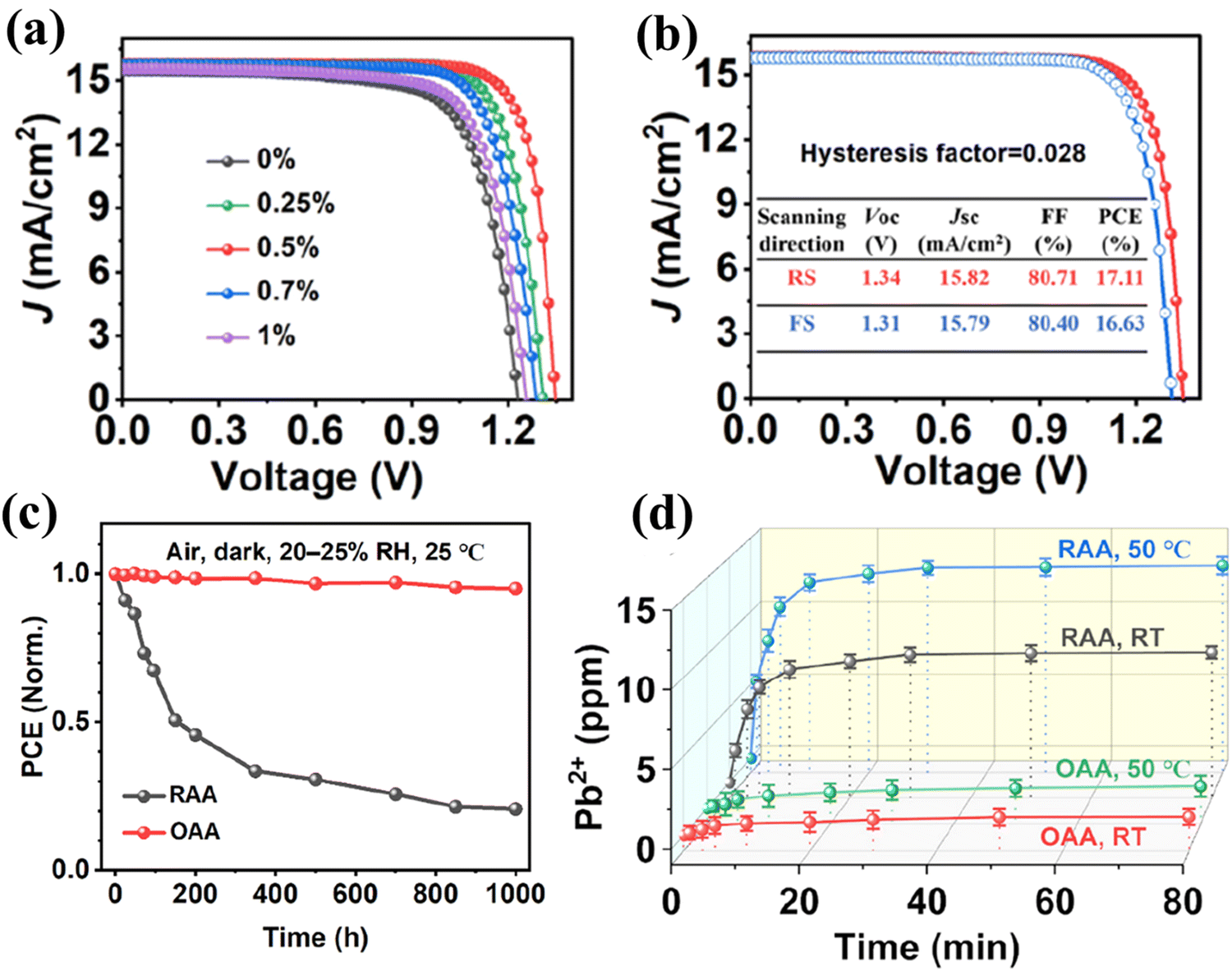 | ||
| Fig. 12 (a) I–V characteristics of PSCs with different concentrations of BP-9 additives. (b) I–V hysteresis. (c) Stability test at 25 °C in ambient air with 20–25% RH with BP-9(OAA) and pristine device (RAA). (d) Pb2+ leakage test into deionized water at room temperature and 50 °C of the additive-induced device and pristine device. Reproduced with permission from ref. 206. | ||
Moreover, the research team headed by J. Xiong incorporated triethyl phosphate (TEP), a cost-effective, efficient, and hydrophobic electron-rich organophosphorus ligand, into an MAPbI3 perovskite layer using antisolvent engineering.209 TEP functions as a defect passivator, a morphology-modifying agent to improve crystallization, and a humidity stabilizer. The phosphate group in TEP establishes robust Pb–O bonds with PVSK, efficiently passivating defects produced during crystallization. Furthermore, the ethyl groups provide hydrophobic protection, safeguarding the PVSK coating from moisture-induced deterioration. The performance of TEP-modified PSC surpassed that of pristine PSC by enhancing the PCE from 15.20% to 19.60. Moreover, during 400 hours at 85% humidity in darkness, the TEP-modified device preserved 82% of its initial PCE, whereas the unmodified PSC retained only 4%. This performance suggests that TEP can effectively bind Pb through its electron-rich phosphate group, thereby enhancing the stability of the PVSK layer. However, the research group did not study the mitigation of lead leakage under water. Furthermore, using a phosphate-containing molecule, hydrogen octylphosphonate potassium (KHOP), the research team under the direction of B. W. Mao investigated a PVSK composition of (FAPbI3)0.9(MAPbI3)0.05 to passivate iodine defects by inhibiting the formation of metallic lead.210 By means of oxygen peaks at 532.2 eV (surface oxygen) and 530.6 eV (phosphate oxygen), an XPS study verified the existence of KHOP. Two Pb 4f spectral peaks in the control sample at 141.9 and 137.0 eV also showed the presence of metallic Pb0 due to iodine defects, which disappeared following KHOP modification, demonstrating its efficacy in preventing the formation of metallic Pb0. Due to this passivation of defects, the KHOP-modified PSC shows a surprisingly reduced hysteresis of 1.33%, compared with the control (6.13%) PSC. Furthermore, the pristine device with the configuration FTO/c-TiO2&m-TiO2-perovskite/Spiro-OMeTAD/Au exhibited a PCE of 18.65, whereas the KHOP-modified device demonstrated a PCE of 22.21%. They demonstrated that, while the passivation of I−-based defects in the PVSK film is satisfied by the interactions of K+ cations of KHOP molecules with the halides of PVSK films, the passivation of lead defects results from the Lewis acid–base interactions between the phosphate groups of KHOP molecules and Pb2+ at the surfaces and grain boundaries of PVSK films. Furthermore, the mild hydrophobic alkyl chain found in the KHOP molecule enhances the stability to moisture of PVSK films as well as the devices. Following tuning, the champion device still maintains 88% of its starting efficiency after 2000 h of storage in dark environmental settings.
 | ||
| Fig. 13 (a) Absorption of lead ions on P@M-4. The two inserted figures show the quantity of absorbed Pb2+ and the pseudo-first-order kinetic model. (b) Pb concentration in contaminated water, detected by ICP-OES. TOF-SIMS depth profiles of PSCs with (c) pristine HTL and (d) HTL-P@M-4. (e) Stability test of the unencapsulated devices in 40% RH and 25 °C. (f) A schematic diagram of the impact of P@M on the performance of the devices. Reproduced with permission from ref. 195. | ||
Another prominent research team comprised of D. Xu and his colleagues fabricated an in situ-crosslinked insoluble polymer (Spiro-NPU) with compatible energy levels, good electrical conductivity, and well-matched hole mobility.211 This Spiro-NPU was composed of 1,5-naphthalene diisocyanate (NDI) and (2,20,20,200′-(((9,90-Spirobi[fluorene]-2,20,7,70-tetrayltetrakis(phenylazanediyl))tetrakis(ethane-2,1-diyl))tetrakis(oxy))tetrakis(-etan-1-ol)) (Spiro-OH) utilized as an internal encapsulation layer between the Spiro-OMeTAD and PVSK layers. They observed that the acylamino groups from Spiro-NPUs can coordinate with Pb2+. They also claimed that they had found 17 ppm of lead after the MAPbI3 film was immersed in deionized water for one hour. On the other hand, they did not see any lead after immersing MAPbI3 film covered with Spiro-NPU for 3 hours. Moreover, the efficiency of the PSCs with Spiro-NPU was enhanced to 21.69% from 20.51%. The essence of this research is depicted in Fig. 14.
 | ||
| Fig. 14 (a)–(c) Comparative stability analysis of PSCs with and without Spiro-NPU internal encapsulation under varied moisture and temperature conditions. (d) Maximum power point (MPP) tracking of PSCs under AM1.5G, 100 mW cm−2 solar spectrum conducted in a glovebox. (e) Water-soaking test for MAPbI3 with and without Spiro-NPU, displaying lead leakage measurements. Reproduced with permission from ref. 211. | ||
Meanwhile, the well-established research team led by S. Wu utilized a thiol-functionalized 2D conjugated MOF with high electron transfer capability and chemical stability as an electron-extraction layer at the interface of PVSK and the cathode in p–i–n-configured PSCs.212 More specifically, they adopted a 2D conjugated Zr(IV)-based MOF with n-type conductivity. The new linker compound holding thiol-group-based ZrL3 made bonds between S and Ag with the top Ag electrode, to decrease the contact resistance. As a result, they observed a better efficiency of 22.02% in contrast to the reference device, which had a PCE of 21.32%. In addition, PSCs modified with a MOF maintained more than 90% of their reference efficiency under continuous light exposure with MPP tracking at 85 °C for 1000hours. More outstandingly, the functionalized MOF was capable of absorbing most of the leaked lead ions from degraded PSCs by making water-insoluble compounds. In particular, ZrL3 displayed a high lead adsorption capability (355 mg g−1) as well as a high sorption rate constant (0.103 min−1). Another prominent research team consisting of J. Chen et al. employed Na3PO4 to modify the ETL SnO2 to enhance its charge transfer capabilities and passivate the buried PVSK interface.196 The compound Na3PO4 passivated Sn dangling bonds in the ETL of the SnO2 layer by making Sn–O–P bonds, which altered the alignment of the energy level to facilitate the extraction of photoelectrons. Consequently, they observed that the modified PSCs showed a higher PCE of 23.06% in comparison to the PCE of 20.39% for the pristine PSCs. In addition, they claimed that they reduced the leakage of lead from PSCs by 80% after utilization of Na3PO4. Similarly, J. Zhang et al. utilized a mixture of amino trimethylene phosphonic acid and KOH (ATMP-K) into the precursor of SnO2 to elevate the performance of the ETL in PSCs.213 They found that ATMP-K successfully passivates oxygen deficiencies and lessens the hydroxyl groups on the ETL surface, which facilitates a larger grain size as well as better alignment of the energy level with PVSKs. ATMP-K improves the efficacy of the devices from ∼21% to ∼24%. In addition, they observed that the SnO2 + ATMP-K film absorbed 50% of Pb2+ while the control SnO2 film adsorbed only 14% of Pb2+ after immersion into water with Pb2+ for 5 days.
:1. Although the PSCs displayed a negligible drop in PCE, they inhibited 98% of lead leakage from the device. In a similar manner, the established researcher Z. Li and his team employed a blend of a CER (C100) and an ultraviolet resin as an encapsulant of PSCs to effectively absorb the leakage of lead.45 In addition, the sulfonic acid group (SO3) in the CER has a greater affinity for Pb2+ than for Na+; therefore C100 easily makes Na+ available to capture Pb2+. Later they used the blended C100 with a conventional UV-curable encapsulant to wrap the PSCs with a cover glass. They claimed that their device was able to reduce 90% of lead leakage from the PSCs when the encapsulated damaged mini-modules were subjected to acidic water. The encapsulation design utilizing CER within the encapsulant layer to effectively prevent lead ion leakage and the impact of CER-based encapsulant are demonstrated in Fig. 15.
 | ||
| Fig. 15 (a) Cation exchange resin (cation exchange between Pb2+ and Na+). (b) Encapsulation design utilizing CER within the encapsulant layer to effectively prevent lead ion leakage. (c) Pb2+ absorption kinetics by the cation exchange resin. The two inserted figures show the quantity of adsorbed Pb2+ and Lagergren first-order kinetics. (d) Temporal Pb2+ concentration profile of glass substrates with a 25:1 UVR/C100 coating versus pure UVR in 10 ppm PbI2 solution; the orange dashed line indicates background Pb2+ in DI water. (e) Temporal Pb2+ concentration profile of the damaged pristine device, with UVR and UVR-C PSCs soaked in 2 mL of DI water at room temperature and 70 °C. (f) Normalized PCE of the pristine device, with UVR and UVR-C PSC encapsulation kept in ambient air for over 500 hours. Reproduced with permission from ref. 45. | ||
The research team of Z. Li et al. employed sulfonated graphene aerogels blended with polydimethylsiloxane to facilitate lead-capturing encapsulants on both sides of PSCs.217 The sulfonated graphene aerogels have exceptional lead adsorption capability in solution owing to their large specific surface area and superior binding energy with Pb2+. More than 99% of Pb2+ from the degraded PSCs can be netted by the encapsulant in various circumstances. After 3000 bending cycles, the PSCs were dipped in deionized water, and they found a concentration of 150 ppm within 30 minutes from the pristine PSCs, whereas it was 9.6 ppb from the encapsulated PSCs.
The renowned researcher X. Zhu and his colleagues introduced an “inner encapsulation” tactic in flexible PSCs by employing a photocurable crosslinkable molecule named benzyl acrylate (BzA).198 The photocurable BzA has the ability to coordinate with Pb2+ by making C![[double bond, length as m-dash]](https://www.rsc.org/images/entities/char_e001.gif) O–Pb bonds. BzA is capable of being polymerized on the surface of PVSK film; consequently, the acrylic group of BzA boosts the water-repelling ability of the film surface along with a reduction in deep shallow-level traps, which leads to control over recombination at interfaces. They achieved an outdoor PCE of 20.86% (0.07 cm2 cell) and 16.75% (24 cm2 module of 8 cells) under illumination by AM1.5G for the flexible device. Moreover, they explored the indoor PCE of the PSC module for the first time and achieved 30.73% for a white LED and 26.48% for a yellow LED under an intensity of 1000 lux. More importantly, the PSC module based on BzA confirmed excellent long-term stability, by retaining 81.0% of the reference efficiency after 400 hours in 75% humidity testing and 84.5% of the original efficiency after 300 hours of lighting at AM1.5G. Furthermore, it displayed mechanical flexibility and stability by retaining 80% of the original efficiency after 3000 bending cycles with a 10 mm radius. Besides, the thick crosslinked BzA layer effectively prevented lead leakage from the PSC when dipped in water.
O–Pb bonds. BzA is capable of being polymerized on the surface of PVSK film; consequently, the acrylic group of BzA boosts the water-repelling ability of the film surface along with a reduction in deep shallow-level traps, which leads to control over recombination at interfaces. They achieved an outdoor PCE of 20.86% (0.07 cm2 cell) and 16.75% (24 cm2 module of 8 cells) under illumination by AM1.5G for the flexible device. Moreover, they explored the indoor PCE of the PSC module for the first time and achieved 30.73% for a white LED and 26.48% for a yellow LED under an intensity of 1000 lux. More importantly, the PSC module based on BzA confirmed excellent long-term stability, by retaining 81.0% of the reference efficiency after 400 hours in 75% humidity testing and 84.5% of the original efficiency after 300 hours of lighting at AM1.5G. Furthermore, it displayed mechanical flexibility and stability by retaining 80% of the original efficiency after 3000 bending cycles with a 10 mm radius. Besides, the thick crosslinked BzA layer effectively prevented lead leakage from the PSC when dipped in water.
In order to assess the leakage of lead ions from the PSC module under acid rain erosion conditions, we submerged unencapsulated PSC modules both with and without a BzA layer in DI water with a pH of roughly 5–6. The lead content for the device without BzA reached 12.3 ppm at ambient temperature and increased much more when heated to 60 °C, suggesting that substantial lead leakage had occurred. On the other hand, the lead content of the BzA-based PSC module decreased significantly to 2.1 ppm, suggesting that BzA showed good capacity to prevent Pb2+ ions from dissolving in water. This has promising implications for preventing environmental pollution due to Pb leakage. The performance of the PSCs and lead leakage from the PSCs with and without BzA under various conditions has been analyzed in Fig. 16.
 | ||
| Fig. 16 (a) ISOS-D-1 stability test results for PSCs with and without BzA, exposed to air with 75% humidity over 400 hours. (b) ISOS-L-1 stability test results comparing PSCs with and without BzA modification, under AM1.5G illumination at 20% relative humidity over 300 hours. (c) Performance analysis of the devices with respect to bending cycles with a 10 mm radius. (d) Dipping test of the devices with and without BzA in DI water with pH between 5 and 6 to mimic acidic rain. (e) Lead concentration leakage from unencapsulated PSCs after 240 minutes of dipping in water. Reproduced with permission from ref. 198. | ||
 | ||
| Fig. 17 (a) Extraction of lead and reuse in a PSC. (b) Reconstruction of PVSK layer and other layers. (c) Percentage of lead recovery using various tactics.225–234 (d) Comparison of recycled lead-based PSCs with fresh lead-based PSCs.235–238 | ||
As an attempt at lead recycling, the famous research group led by C. G. Poll used a deep eutectic solvent made of ethylene glycol and choline chloride for the first time to extract the lead from MAPbI3, MAPbI3−xClx or FAPbI3, through dissolution and selective electrodeposition.44 They confirmed that the lead cation is enclosed by three chlorine atoms at a 2.65 Å distance. More specifically, the most likely Pb species in the DES is [PbCl3]−. In addition, they claimed that the process was able to achieve an outstanding recovery rate of up to 99.8% of lead elimination from the solution with eutectic solvent via electrochemical deposition. Additionally, the renowned researcher A. Binek and his colleagues employed a method for recycling Pb and reusing FTO from solar devices with a configuration of glass/FTO/TiO2/MAPbI3/Spiro-OMeTAD/Au.199 According to this approach, the PSCs were broken down layer by layer. After eliminating the Au and HTL, the PVSK film of the PSC was immersed in distilled water to convert it into PbI2 and MAI in water. Subsequently, MAI was obtained from the water. Due to the short time of immersion and low solubility of PbI2 in water, DMF was added with PbI2 to dissolve and reuse it. The recycled PbI2 solution and FTO substrate were then utilized in the production of fresh PSCs. The PSCs made from the recovered materials exhibited an efficiency of 13.5%, which is slightly lower than that for PSCs (14.6%) made from highly pure PbI2. The reduced PCE was likely to be due to the presence of very few impurities in the recycled PbI2. A research team comprised of S. Zhang et al. established an eco-friendly dissolving–precipitating technique for the cyclic utilization of lead from carbon-based PSCs with the configuration glass/FTO/c-TiO2/m-TiO2/MAPbI3/carbon.200 They used DMF to dissolve solar devices and obtain lead with lixivium. In addition, NH3·H2O was employed as a precipitator to extract Pb2+ from lixivium. The findings scrutinized by inductively coupled plasma optical emission show that roughly 99.9% of the lead could be extracted by NH3·H2O. Later, HI was utilized to produce PbI2. They found that a small amount of PbI2 was converted into [PbI4]2− owing to the low concentration of HI. The estimated lead recovery rate was 95.7%. Finally, a new PSC was fabricated by employing the recycled PbI2 and attained an efficiency of 11.36%, which was a little bit lower than that of PSCs (12.17%) fabricated from commercial PbI2. This drop in PCE might be attributed to the poorer purity of recycled PbI2 in comparison with commercial PbI2, which also indicates the impurities remaining in PbI2 at the time of precipitation. In addition, the Pb lixivium is a combination of dissolved HTMs and PVSK, since DMF dissolves both PVSK and HTM.
Another research group led by J. Xu, devised an in situ PbI2 recycling technique, which represents a step toward sustainable PSCs.239 They studied the thermal characteristics of MAPbI3 films on an m-TiO2/c-TiO2/FTO/glass substrate. Their findings revealed a PbI2 mesoporous configuration with good crystallinity and a broad domain. Firstly, they removed HTM from PSC by immersing it in chlorobenzene and decomposed the PVSK into mesoporous PbI2 and organic gases by adopting heat treatment. Subsequently, a fresh PVSK film was made by employing MAI through the spin-coating technique. Due to the mesoporous structure of PbI2, it facilitates effective contact between MAI and PbI2. Therefore, the PCE of the rejuvenated PSCs was augmented from 14.35% to 14.84%. This heightened PCE can be ascribed to the increased PVSK loading of the nanostructured scaffold and the bi-layered PVSK configuration created during the regeneration approach, which allows for effective light trapping. However, the efficiency of the double-regenerated device was lowered to 8.51% because of the excess residual PbI2 and lower surface coverage.
Designing a procedure to recycle and recover target materials from degraded devices requires a comprehensive strategy. The well-known researcher B. J. Kim and his co-workers developed a strategy to isolate most major components of PSCs, including lead from PVSK, ETL, HTL, electrode, and TCO, simultaneously.240 The procedure of selectively dissolving m-TiO2-coated FTO substrates in PSCs consists of many simple stages. First, the trihalide PVSK and Spiro-OMeTAD are separated by submersing the devices in a polar aprotic solvent (PAS) like DMF, DMSO or GBL and shaking them for 30 s. Then the substrates are washed, rinsed with DI water, and annealed at 500 °C for an hour for further improvement in performance. The gold in PSCs is non-reactive with PASs; therefore any gold that remains in solution after cleaning can be recovered. In addition, the lead is removed from the PAS by adopting a two-step recycling process including solvent extraction and an ion exchange technique. A 0.05 molarity MAPbI3 solution in DMF is poured into ether, a non-polar solvent, which separates the precipitated lead compound. The lead component is isolated and then centrifuged for 10 minutes at 8000 rpm. A laboratory-prepared (Ca10(PO4)6(OH)2) powder is then added to the rest of the solution to eliminate leftover Pb2+ ions by ion exchange from Ca2+ to Pb2+. After stirring the solution at 200 rpm for 3 hours, the Pb2+-ion-adsorbed (Ca10(PO4)6(OH)2) powder is isolated by centrifugation at 8000 rpm for 10 minutes. They claimed that almost 99.99% Pb content from the blended solution was removed by employing this technique. Moreover, they fabricated PSCs by utilizing the recycled material and obtained comparable results to fresh material. Another research group led by J. M. Kadro proposed an approach for the recycling and recovery of solar devices that involves the layer-by-layer breakdown and recovery of most main components.241 A PSC with the structure glass/FTO/c&m-TiO2/MAPbI3/Spiro-OMeTAD/Au underwent a treatment process where chlorobenzene was used to dissolve the HTL, which also allows for recycling of Au. Subsequently, ethanol was adopted to eliminate MAI, leaving behind PbI2 from MAPbI3. The PbI2 remaining on the glass/FTO/c-TiO2/m-TiO2 substrate was then recycled using DMF. To recover Pb from the mixed DMF solution, Payne's electrodeposition technique was suggested. They perceived that methanol facilitates the quickest conversion from MAPbI3 to PbI2 among the solvents tested. This was followed by deionized water, ethanol, and 2-propanol in terms of conversion speed. Ethyl acetate, on the other hand, was the slowest, taking several hours for complete MAI dissolution, thus rendering it impractical for use. Ethanol was preferred over methanol for device recycling due to its lower toxicity for humans and the ecosystem, despite its slower dissolution rate, and because it dries faster than water. The lead content within every solvent was evaluated by utilizing inductively coupled plasma mass spectrometry to evaluate their selectivity in lead sequestration. Water performed with the highest selectivity, showing only 0.14% of the total lead content, similar to chlorobenzene. After purification with Amberlite 120 IR resin, the lead content in water dropped to 0.03%, although lead sequestration by the resin might be limited at very low concentration. A saturated PbI2 solution in water with a 30-fold molar excess of MAI displayed a lead concentration of 43.5 ppm, which reduced to 0.44 ppm after 16 hours of resin treatment, indicating a 99% sequestration efficiency. The 2-propanol confirmed the second-best selectivity with 0.35% lead content, but its slower MAI dissolution time (about 20 minutes) made it less suitable. Ethanol resulted in up to 3.4% lead content, and methanol had the poorest performance with up to 7% lead content. Ion exchange resins like Amberlite IR 120 can purify organic solvents, including methanol and IPA.242,243 An effective electrochemical method for lead recovery from PSCs has been explained, involving the electrodeposition of lead using ethylene glycol with choline chloride as the solvent.244 However, the device performance with the recycled FTO/TiO2 substrate was 15–16% PCE along with Jsc ranging from 19.7 mA cm−2 to 21.5 mA cm−2.
Another research study conducted by X. Tao et al. describes an environmentally benign approach for upcycling sustainable PSCs using optimal lead recovery and recycling.201 The procedure entails screening of Pb-solubilizers (BA, DMF, and DMSO) and employing KI precipitation. DMF was chosen as the best solubilizer due to its high Pb-dissolution capacity and low Pb-adhesion, resulting in a PbI2 purity of 96.03%. DMF is also recoverable for reuse, which improves sustainability. The recovered PbI2, ITO, and Ag components were effectively utilized in PSC manufacturing. Notably, the recycled PSC had a PCE of 22.78% that is higher than the 20.76% PCE of PSCs built from new components. After four recycling cycles, the refabricated PSC still had a PCE of 20.79%, equivalent to that of fresh PSCs. The detailed performance metrics are depicted in Fig. 18.
 | ||
| Fig. 18 (a) and (b) J–V characteristics of fresh and recycled PSC. (c) SPO values measured at MPP for both fresh and recycled PSC. Stability of the unencapsulated fresh and recycled PSC (d) under air atmosphere for 1200 h (RH = 60–80%), (e) under nitrogen atmosphere at 85 °C for 1200 h and (f) under one-sun illumination in air and MPP tracking. (g) Cycling stability of the regenerated PSC. Reproduced with permission from ref. 201. | ||
The aforementioned approaches are able to tackle the issue of lead in PSCs, and the Pb recovery rates in these studies were acceptable. However, the efficiencies of solar devices made with recycled components, especially PbI2, were somewhat lower than those made with new PbI2. The impurities in recycled components have been labeled a possible cause of the degraded efficiency. Thus, purification methods for recycled materials, along with recycling and recovery approaches, need to be optimized to prepare for large amounts of end of life (EOL) solar devices. Furthermore, although more complex PSC structures, like Cs0.05(MA0.17FA0.83)0.95Pb(I0.83Br0.17)3, demonstrate superior PCEs and stability, extracting and purifying high-quality Pb-containing materials from PSCs is a major challenge.245,246 The lead-acid battery industry has established advanced Pb recycling technologies consisting of electrodeposition and precipitation.247–249 Consequently, Pb recycling and recovery from PSCs may offer greater industrial potential applications along with other PSC components.
The cost contribution of the PVSK layers, composed from lead-based compounds, is relatively lower than that of other PVSKs like germanium-based PVSKs and other components of a PSC. As a result, their (lead-based) recycling holds minimal economic interest, and the reason for that lower interest is depicted in Fig. 19. However, due to environmental concerns associated with lead-containing materials, the focus shifts toward recycling PbI2 to mitigate its ecological impact. Additionally, from an economic perspective, the recovery and reuse of FTO/ITO-coated glass, HTM, ETM, and electrodes are valuable.
 | ||
| Fig. 19 A pie chart illustrating the projected expenses associated with the various layers in PSCs. Redrawn with permission from ref. 250. | ||
4. Potential hazardousness of incorporated substances
During the replacement of lead within the PVSK framework, researchers must carefully assess the toxicity levels of substituting elements compared to lead. Fig. 2(a) presents a comparison of the health effects of various elements considered potential lead replacements, where Pb, Cd, and Hg exhibit significant health hazards. Based on this analysis, suitable alternatives to lead can be discovered. Furthermore, the research community should also prioritize evaluating the environmental and health impacts of other materials used in PSCs, including additives, solvents employed during the fabrication of fresh PSCs, and the recovery and recycling of different components of PSCs. Our observations indicate that the additive compounds included in Table 6 and Table S1 (ESI†) demonstrate various degrees of toxicity, from low to high, with associated risks, such as neurotoxicity, carcinogenicity, respiratory complications, organ toxicity, and environmental persistence. By taking appropriate protective measures with adequately ventilated spaces, safety can be ensured. However, environmental factors must be considered, since a few persistent chemicals may lead to enduring ecological harm. Moreover, comprehending the toxicity profile of these compounds is essential for creating safer formulations, reducing occupational risks, and guaranteeing regulatory adherence in industrial and research contexts. Consequently, thorough risk evaluations, the discovery of alternative materials, and compliance with safety regulations must be prioritized in any research employing these compounds.| Group | Material | Nature of toxicity | Ref. |
|---|---|---|---|
| Carbonyl | Poly(butylene adipate-co-terephthalate) (PBAT) polymer | Although PBAT is not poisonous, its breakdown products, adipic acid and terephthalic acid, can harm the environment and microbial soil populations, impacting ecosystem health. | 251 and 252 |
| Thiol | Thiol group of 1H,1H,2H,2H-perfluorodecanethiol | It may cause skin, eye, and liver irritation. It may also be harmful if swallowed. | https://www.sigmaaldrich.com/MY/en/product/aldrich/660493 |
| Sulfonic acid | Phenylbenzimidazole sulfonic acid | It is a UV-B absorber used in cosmetics and sunscreens. It can cause skin irritation and allergic reactions. | 253 |
| Aniline | Ligand molecule 4-[(trifluoromethyl)sulfanyl]-aniline (4TA) with trifluoromethyl (–CF3) and aniline (–NH2) moieties | The increased lipophilicity of the trifluoromethyl group and the possible reactivity of the aniline group—which might disturb cellular functions—cause it to be poisonous. | https://www.sigmaaldrich.com/MY/en/product/aldrich/224936 |
| https://pubchem.ncbi.nlm.nih.gov/compound/9964 | |||
| Spiro-NPU | 1,5-Naphthalene diisocyanate (NDI) and (2,20,20,200′-(((9,90-Spirobi[fluorene]-2,20,7,70-tetrayltetrakis(phe-nylazanediyl))tetrakis (ethane-2,1-diyl))tetrakis(oxy))tetrakis(-etan-1-ol)) (Spiro-OH) | Spiro-NPU contains NDI, a respiratory sensitizer and irritant that can cause respiratory difficulties, skin and eye irritation, allergic responses, and long-term damage to aquatic life. Inhalation can be lethal. | https://echa.europa.eu/substance-information/-/substanceinfo/100.019.675 |
| Phosphate compounds | Na3PO4 | It can cause kidney damage, skin irritation, and respiratory issues. | (1) https://core-docs.s3.amazonaws.com/documents/asset/uploaded_file/234350/Sodium_Phosphate_Tribasic.pdf |
| (2) https://medlineplus.gov/druginfo/meds/a609019.html#:~:text=Sodium%20phosphate%20can%20cause%20serious,%2C%20decreased%20urination%2C%20and%20headache. | |||
| Acrylate-based materials | Butyl acrylate | The main hazard of BA is its ability to irritate skin, eyes, and respiratory tract upon contact or inhalation. | 254 |
| Aromatic solvents | Chlorobenzene | It can affect the central nervous system, liver, kidneys, and other organ systems. | (1) https://www.nj.gov/health/eoh/rtkweb/documents/fs/0379.pdf |
| (2) https://wwwn.cdc.gov/tsp/substances/ToxSubstance.aspx?toxid=87 | |||
| Solvent | DMSO | DMSO is a cryoprotectant that can cause serious side effects, including fatal arrhythmias, respiratory arrest, and seizures. | 255 and 256 |
5. Perspective and prospects
The remarkable achievements in the performance of lead-based PVSKs within a very short period are overshadowed by the environmental and health hazards posed by poisonous lead. Lead-free PVSKs are now being projected as the next breakthrough in the evolution of PSCs. Accordingly, extensive research endeavors have been conducted to replace lead or lower the leaching of lead into the environment from PSCs by adopting various approaches. Many research groups suggested that Sn, Ge, Bi, Sb, etc. could be promising alternatives to lead in PVSK structures, because of their similar structures to lead with ns2 lone pairs, which can form octahedra with halogen anions. Theoretical studies and experimental electro-optical characterization suggest that Sn-based PVSK shows comparable carrier lifetime and diffusion length to lead-based PVSK. Sn-based PSCs show a glimmer of hope by achieving a noticeable efficiency of 15.38%, although this is far from the value for lead-based PSCs. However, Sn2+ is easily converted into Sn4+. The level of Sn2+ oxidation is greatly influenced by the surrounding chemical environment in the precursor and crystal lattice. Thus, investigating of composition engineering at A- and X-sites can minimize Sn2+ oxidation and greatly boost the performance and stability of Sn-based solar devices.On the other hand, a similar problem of stability in Sn-based PVSK, namely the oxidation of Ge2+ to Ge4+, is also a significant concern with Ge-based halide PVSKs. Currently, the PCE of Ge-based PSCs is below 5%, hindered by factors such as a smaller ionic radius, limited solubility in polar solvents, and a relatively large bandgap. However, PVSKs based on Ge have not yet received considerable experimental interest because of the aforementioned limitations. Recent theoretical and experimental research suggests that a Ge–Sn combination might be a feasible choice for upgrading the performance of Ge2+-based PSCs. So far, the highest efficiency recorded for mixed Ge–Sn materials is around 7.9%. However, Sn- or Ge-based PVSKs decay faster than lead-based PVSKs.
To overcome this, tactics such as employing bilayer PVSKs (e.g., Bi3+/Sb3+) to prevent phase changes induced by ion migration, delaying crystallization, suppressing oxidation by additive engineering, or synthesizing double PVSKs can be applied. Most HDPs typically have relatively larger bandgaps than Pb-based PVSKs (usually greater than 1.8 eV). This feature is generally undesirable for single-junction photovoltaics, although it can be advantageous for tandem SCs. At present, the PCE of HDP-based (Cs2AgBiBr6) PSCs is around 6.37%, which is also far from the value for lead-based PSCs. Despite earnest efforts to enhance overall PCE, it remains considerably lower than for Pb-based SCs. Therefore, the continuous systematic exploration of abundant composition options for Pb-free halide PVSKs can expand the range of absorber materials and boost performance by expediting the advancement of eco-friendly and cost-effective Pb-free PSCs through material genome approaches and innovative device designs.
On the other hand, some researchers have proposed chalcogenide and metal-free organic PVSKs as promising emerging photovoltaic materials due to their exceptional optoelectronic properties, supported by both theoretical and experimental studies. However, their research is still in its early stages for photovoltaic applications. To further improve performance, key inherent challenges must be addressed, such as enhancing material stability, exploring novel synthetic methods, designing appropriate device structures, and gaining a deeper understanding of the photodynamics and underlying functional mechanisms.
As lead-based PSCs performed better with a PCE of 26.7% than lead-free PSCs with a PCE of 15.38% along with superior stability, the scientific community is eager to enjoy the excellent performance from lead-based PSCs, notwithstanding their toxicity. Those researchers are working on the confinement of lead within host materials to lessen the leakage of lead from PSCs in conjunction with attempts to produce lead-free PSCs. Consequently, many approaches have emerged to lower the toxicity risk of lead by mitigating lead leakage from PSC modules, including an additive approach for chelation, modification of charge transporting layers, encapsulation by lead-capturing functionality, and lead management at the end of life of PSCs. In the case of lead-immobilization strategies, encapsulation by lead-capturing functionality is generally more effective than complexation in reducing Pb leakage. Conversely, complexation offers additional benefits, including improved crystallinity and defect passivation, which ultimately enhance performance. Encapsulation effectively inhibits lead leakage following damage, but it does not contribute to improving the intrinsic performance of PVSK materials. That is why research on PVSK materials should be focused more on compositional engineering, the adoption of lower-dimensional structures, and the strategic application of performance-enhancing additives to bring about intrinsic stability.
Incorporating functional molecules or dopants can help passivate defects, reduce ion migration, and improve optoelectronic characteristics. These techniques not only enhance device performance, but they also solve crucial moisture and thermal stability issues. Therefore, more systematic studies are needed to explore the roles of different functional groups or dopants from various perspectives. Similar strategies should also be utilized for Pb-chelating charge-transport compounds. Encapsulation with Pb-chelating materials appears promising for achieving Pb leakage levels that are safe for use. However, thorough research is essential to confirm that materials with different functional groups used for chelating or capturing lead are environmentally safe. In addition, the lead-suppression efficiency of an absorbent material may be hindered by factors such as sorption kinematics, environmental variations (pH, temperature), and interference from other ions. Test conditions, like temperature and water exposure methods, greatly influence lead leakage and adsorption. To enable an accurate evaluation and comparison of lead leakage from PSCs across global findings, a standardized lead-leakage testing protocol should be developed. This would ensure consistent assessment of various lead-confinement techniques under uniform conditions.
Moreover, the degradation or damage of lead-based PSCs poses significant environmental concerns because of the risk of toxic Pb leakage at the end of their lifespan. The recycling of lead compounds at the end of their life or after their damage has emerged as a critical research topic for long-term use with little environmental impact. To date, several prominent researchers have focused on Pb recycling and fabricated PSCs utilizing recycled lead. They obtained PCEs that are comparable to those of the original PSCs, which indicates their potential as a promising strategy for practical application. However, attention should be given to eco-friendly solvents for dissolving the lead-containing materials and an evaluation of the environmental impact of recycling processes to ensure overall sustainability.
Therefore, the ideal solution would be to completely replace lead-containing PVSK materials with eco-friendly PVSK compounds with desirable performance. However, due to the suboptimal performance of lead-free PSCs, this approach may demand extensive research, along with a considerable investment of time and resources. Therefore, practical risk management strategies for dominant lead-based PSCs are essential to ensure the usage of PSCs that are economically viable, sustainable, and eco-friendly. In addition, technologies that increase the public acceptability of the present Pb-based PSCs demand further development.
6. Conclusion
PVSK solar cells have emerged as a leading contender among emerging photovoltaic technologies by achieving an impressive PCE of 26.7%. However, the environmental concerns associated with the lead content in PSCs require the development of effective tactics to mitigate lead-related risks. In this review, various tactics have been discussed to overcome this issue, implemented by different prominent research groups, including replacing lead in the ABX3 structure with isoelectronic elements, confining lead within the PVSK matrix using functional molecules or dopants, integrating lead-absorbent materials into charge carrier transport layers, and employing encapsulation techniques with lead-capturing materials. As the replacement of lead by isoelectronic alternatives has not matched the performance of lead-based PSCs, the scientific community is enthusiastic about enjoying the excellent performance from lead-based PSCs by implementing lead-confinement strategies along with keeping a focus on the replacement of lead in the PVSK framework. Among all attempts at lead confinement inside a device, the incorporation of functional molecules or dopants not only confines lead within the PVSK framework, but also enhances the stability and performance of the PSCs by confirming improved crystal quality. On the other hand, encapsulation effectively prevents lead leakage, but it does not contribute to intrinsic improvements in the photovoltaic properties of the material. Therefore, future research should focus on compositional engineering, the adoption of lower-dimensional entities and the development of multifunctional additives that simultaneously improve the stability, efficiency, and environmental safety of PSCs. Furthermore, recycling approaches for PSCs have been studied by showcasing methods to extract lead from damaged devices and reuse it in fresh PSCs. These refabricated devices presented comparable PCEs with reduced cost and promoted environmental safety. Such initiatives highlight the potential for sustainable and environmentally responsible practices in PVSK solar technology. In the final part of this review, a comprehensive perspective and future direction on the various approaches to addressing lead-related challenges in PSCs were provided. By reviewing the successes, limitations, and future directions, we believe that these insights will advance the understanding of lead mitigation in PSCs, encouraging the development of safer, more sustainable photovoltaic technologies.Author contributions
Md. Helal Miah, Md. Jakir Hossen, Noor-E-Ashrafi and Ismat Jahan: conceptualization, literature review, performed study, data analysis and writing of original draft, Mohammad Aminul Islam, Mohammad Nur-E-Alam, Mohamed Y. Hanfi, Md. Habib Ullah & Md. Shahinuzzaman: data curation, discussion, software and validation, Mayeen Uddin Khandaker: supervision, and reviewing and editing of the manuscript.Consent for publication
All authors of this work have agreed and are ready to sign the Transfer of Copyright which empowers the Publisher to protect the work against unauthorized use and to maintain the integrity of the work from a bibliographical and archival standpoint.Declaration of generative AI and AI-assisted technologies in the writing process
During the preparation of this work, the authors used some online services (such as Grammarly, Gemini, etc.) in order to improve language and readability. After using this tool/service, the authors reviewed and edited the content as needed and take full responsibility for the content of the publication.Data availability
All data are available in the manuscript.Conflicts of interest
The authors declare that they have no known competing financial interests or personal relationships that could have appeared to influence the work reported in this paper.Acknowledgements
Sunway University PhD Scholarship support received by Md. Helal Miah is acknowledged.References
- Z. Yang, et al., Roles of Interfacial Tension in Regulating Internal Organization of Low Bandgap Polymer Bulk Heterojunction Solar Cells by Polymer Additives, Adv. Mater. Interfaces, 2018, 5(15), 1800435, DOI:10.1002/ADMI.201800435.
- N. K. Noel, et al., Lead-free organic–inorganic tin halide perovskites for photovoltaic applications, Energy Environ. Sci., 2014, 7(9), 3061–3068, 10.1039/C4EE01076K.
- M. H. Miah, M. U. Khandaker, M. B. Rahman, M. Nur-E-Alam and M. A. Islam, Band gap tuning of perovskite solar cells for enhancing the efficiency and stability: issues and prospects, RSC Adv., 2024, 14(23), 15876–15906, 10.1039/D4RA01640H.
- M. H. Miah, et al., Key degradation mechanisms of perovskite solar cells and strategies for enhanced stability: issues and prospects, RSC Adv., 2025, 15(1), 628–654, 10.1039/D4RA07942F.
- H. Zsiborács, et al., Intermittent Renewable Energy Sources: The Role of Energy Storage in the European Power System of 2040, Electronics, 2019, 8(7), 729, DOI:10.3390/ELECTRONICS8070729.
- H. Min, et al., Perovskite solar cells with atomically coherent interlayers on SnO2 electrodes, Nature, 2021, 598(7881), 444–450, DOI:10.1038/s41586-021-03964-8.
- A. Kojima, K. Teshima, Y. Shirai and T. Miyasaka, Organometal halide perovskites as visible-light sensitizers for photovoltaic cells, J. Am. Chem. Soc., 2009, 131(17), 6050–6051, DOI:10.1021/JA809598R/SUPPL_FILE/JA809598R_SI_001.PDF.
- M. A. Green, et al., Solar cell efficiency tables (Version 63), Prog. Photovoltaics Res. Appl., 2024, 32(1), 3–13, DOI:10.1002/PIP.3750.
- M. A. Green, et al., Solar cell efficiency tables (Version 64), Prog. Photovoltaics Res. Appl., 2024, 32(7), 425–441, DOI:10.1002/PIP.3831.
- A. Babayigit, A. Ethirajan, M. Muller and B. Conings, Toxicity of organometal halide perovskite solar cells, Nat. Mater., 2016, 15(3), 247–251, DOI:10.1038/nmat4572.
- G. Y. Kim, K. Kim, H. J. Kim, H. S. Jung, I. Jeon and J. W. Lee, Sustainable and environmentally viable perovskite solar cells, EcoMat, 2023, 5(4), e12319, DOI:10.1002/EOM2.12319.
- K. P. Goetz, A. D. Taylor, Y. J. Hofstetter and Y. Vaynzof, Sustainability in Perovskite Solar Cells, ACS Appl. Mater. Interfaces, 2021, 13(1), 1–17, DOI:10.1021/ACSAMI.0C17269/ASSET/IMAGES/MEDIUM/AM0C17269_0007.GIF.
- J. Li, et al., Biological impact of lead from halide perovskites reveals the risk of introducing a safe threshold, Nat. Commun., 2020, 11(1), 1–5, DOI:10.1038/s41467-019-13910-y.
- H. Needleman, Lead poisoning, Annu. Rev. Med., 2004, 55, 209–222, DOI:10.1146/ANNUREV.MED.55.091902.103653/CITE/REFWORKS.
- J. Dressier, K. A. Kim, T. Chakraborti and G. Goldstein, Molecular mechanisms of lead neurotoxicity, Neurochem. Res., 1999, 24(4), 595–600, DOI:10.1023/A:1022596115897/METRICS.
- P. C. Hsu and Y. L. Guo, Antioxidant nutrients and lead toxicity, Toxicology, 2002, 180(1), 33–44, DOI:10.1016/S0300-483X(02)00380-3.
- X. Li, F. Zhang, H. He, J. J. Berry, K. Zhu and T. Xu, On-device lead sequestration for perovskite solar cells, Nature, 2020, 578(7796), 555–558, DOI:10.1038/s41586-020-2001-x.
- F. Hao, C. C. Stoumpos, D. H. Cao, R. P. H. Chang and M. G. Kanatzidis, Lead-free solid-state organic–inorganic halide perovskite solar cells, Nat. Photonics, 2014, 8(6), 489–494, DOI:10.1038/nphoton.2014.82.
- S. Y. Park, et al., Sustainable lead management in halide perovskite solar cells, Nat. Sustainability, 2020, 3(12), 1044–1051, DOI:10.1038/s41893-020-0586-6.
- A. Abate, Perovskite solar cells go lead free, Joule, 2017, 1(4), 659–664, DOI:10.1016/j.joule.2017.09.007.
- R. S. Drago, Thermodynamic evaluation of the inert pair effect, J. Phys. Chem., 1958, 62(3), 353–357, DOI:10.1021/J150561A027/ASSET/J150561A027.FP.PNG_V03.
- M. Konstantakou and T. Stergiopoulos, A critical review on tin halide perovskite solar cells, J. Mater. Chem. A, 2017, 5(23), 11518–11549, 10.1039/C7TA00929A.
- Z. Zhao, et al., Mixed-Organic-Cation Tin Iodide for Lead-Free Perovskite Solar Cells with an Efficiency of 8.12%, Adv. Sci., 2017, 4(11), 1700204, DOI:10.1002/ADVS.201700204.
- T. Bin Song, et al., Importance of reducing vapor atmosphere in the fabrication of Tin-based perovskite solar cells, J. Am. Chem. Soc., 2017, 139(2), 836–842, DOI:10.1021/JACS.6B10734/SUPPL_FILE/JA6B10734_SI_001.PDF.
- J. Chen, et al., Efficient tin-based perovskite solar cells with trans-isomeric fulleropyrrolidine additives, Nat. Photonics, 2024, 1–7, DOI:10.1038/s41566-024-01381-7.
- X. Zhou, et al., Additive engineering with 2,8-dibromo-dibenzothiophene-S,S-dioxide enabled tin-based perovskite solar cells with 14.98% power conversion efficiency, Energy Environ. Sci., 2024, 17(8), 2837–2844, 10.1039/D3EE03359G.
- J. Huang, et al., High-Efficiency and Ultra-Stable Cesium–Bismuth-Based Lead-free Perovskite Solar Cells without Modification, J. Phys. Chem. Lett., 2024, 15(12), 3383–3389, DOI:10.1021/ACS.JPCLETT.4C00310.
- B. Bin Yu, et al., Heterogeneous 2D/3D Tin-Halides Perovskite Solar Cells with Certified Conversion Efficiency Breaking 14%, Adv. Mater., 2021, 33(36), 2102055, DOI:10.1002/ADMA.202102055.
- K. Nishimura, et al., Lead-free tin-halide perovskite solar cells with 13% efficiency, Nano Energy, 2020, 74, 104858, DOI:10.1016/J.NANOEN.2020.104858.
- M. A. Kamarudin, et al., Suppression of charge carrier recombination in lead-free tin halide perovskite via Lewis base post-treatment, J. Phys. Chem. Lett., 2019, 10(17), 5277–5283, DOI:10.1021/ACS.JPCLETT.9B02024/SUPPL_FILE/JZ9B02024_SI_001.PDF.
- E. Jokar, et al., Robust Tin-Based Perovskite Solar Cells with Hybrid Organic Cations to Attain Efficiency Approaching 10%, Adv. Mater., 2019, 31(2), 1804835, DOI:10.1002/ADMA.201804835.
- W. Ke, et al., Dopant-Free Tetrakis-Triphenylamine Hole Transporting Material for Efficient Tin-Based Perovskite Solar Cells, J. Am. Chem. Soc., 2018, 140(1), 388–393, DOI:10.1021/JACS.7B10898/SUPPL_FILE/JA7B10898_SI_001.PDF.
- W. Liao, et al., Lead-free inverted planar formamidinium tin triiodide perovskite solar cells achieving power conversion efficiencies up to 6.22%, Adv. Mater., 2016, 28(42), 9333–9340, DOI:10.1002/ADMA.201602992.
- F. Jiang, et al., Chlorine-Incorporation-Induced Formation of the Layered Phase for Antimony-Based Lead-Free Perovskite Solar Cells, J. Am. Chem. Soc., 2018, 140(3), 1019–1027, DOI:10.1021/JACS.7B10739/SUPPL_FILE/JA7B10739_SI_001.PDF.
- Y. Yang, et al., Dimension-Controlled Growth of Antimony-Based Perovskite-like Halides for Lead-Free and Semitransparent Photovoltaics, ACS Appl. Mater. Interfaces, 2020, 12(14), 17062–17069, DOI:10.1021/ACSAMI.0C00681/SUPPL_FILE/AM0C00681_SI_001.PDF.
- A. Singh, et al., Panchromatic heterojunction solar cells for Pb-free all-inorganic antimony based perovskite, Chem. Eng. J., 2021, 419, 129424, DOI:10.1016/J.CEJ.2021.129424.
- W. Gao,
et al., High-Quality Cs2AgBiBr6 Double Perovskite Film for Lead-Free Inverted Planar Heterojunction Solar Cells with 2.2% Efficiency, ChemPhysChem, 2018, 19(14), 1696–1700, DOI:10.1002/CPHC.201800346.
- X. Yang, et al., Multifunctional Dye Interlayers: Simultaneous Power Conversion Efficiency and Stability Enhancement of Cs2AgBiBr6 Lead-Free Inorganic Perovskite Solar Cell through Adopting a Multifunctional Dye Interlayer (Adv. Funct. Mater. 23/2020), Adv. Funct. Mater., 2020, 30(23), 2070147, DOI:10.1002/ADFM.202070147.
- B. Li, et al., Efficient and stable Cs2AgBiBr6 double perovskite solar cells through in situ surface modulation, Chem. Eng. J., 2022, 446, 137144, DOI:10.1016/J.CEJ.2022.137144.
- L. Yang, et al., Performance improvement of dye-sensitized double perovskite solar cells by adding Ti3C2Tx MXene, Chem. Eng. J., 2022, 446, 136963, DOI:10.1016/J.CEJ.2022.136963.
- Z. Zhang, et al., Hydrogenated Cs2AgBiBr6 for significantly improved efficiency of lead-free inorganic double perovskite solar cell, Nat. Commun., 2022, 13(1), 1–12, DOI:10.1038/s41467-022-31016-w.
- X. Wu, et al., Eco-friendly perovskite solar cells: From materials design to device processing and recycling, EcoMat, 2023, 5(7), e12352, DOI:10.1002/EOM2.12352.
- M. A. Green, et al., Solar cell efficiency tables (Version 63), Prog. Photovoltaics Res. Appl., 2024, 32(1), 3–13, DOI:10.1002/PIP.3750.
- C. G. Poll, G. W. Nelson, D. M. Pickup, A. V. Chadwick, D. J. Riley and D. J. Payne, Electrochemical recycling of lead from hybrid organic–inorganic perovskites using deep eutectic solvents, Green Chem., 2016, 18(10), 2946–2955, 10.1039/C5GC02734A.
- Z. Li, et al., An effective and economical encapsulation method for trapping lead leakage in rigid and flexible perovskite photovoltaics, Nano Energy, 2022, 93, 106853, DOI:10.1016/J.NANOEN.2021.106853.
- B. Niu, et al., Mitigating the Lead Leakage of High-Performance Perovskite Solar Cells via in Situ Polymerized Networks, ACS Energy Lett., 2021, 6(10), 3443–3449, DOI:10.1021/ACSENERGYLETT.1C01487/SUPPL_FILE/NZ1C01487_SI_001.PDF.
- G. Y. Kim, K. Kim, H. J. Kim, H. S. Jung, I. Jeon and J. W. Lee, Sustainable and environmentally viable perovskite solar cells, EcoMat, 2023, 5(4), e12319, DOI:10.1002/EOM2.12319.
- P. Photovolt and M. A. Green, Silicon photovoltaic modules: a brief history of the first 50 years, Prog. Photovoltaics Res. Appl., 2005, 13(5), 447–455, DOI:10.1002/PIP.612.
- B. J. Kim, S. Lee and H. S. Jung, Recent progressive efforts in perovskite solar cells toward commercialization, J. Mater. Chem. A, 2018, 6(26), 12215–12236, 10.1039/C8TA02159G.
- M. Younas, M. A. Gondal, M. A. Dastageer and K. Harrabi, Efficient and cost-effective dye-sensitized solar cells using MWCNT-TiO2 nanocomposite as photoanode and MWCNT as Pt-free counter electrode, Sol. Energy, 2019, 188, 1178–1188, DOI:10.1016/J.SOLENER.2019.07.009.
- M. Younas, T. A. Kandiel, A. Rinaldi, Q. Peng and A. A. Al-Saadi, Ambient-environment processed perovskite solar cells: A review, Mater. Today Phys., 2021, 21, 100557, DOI:10.1016/J.MTPHYS.2021.100557.
- N. J. Jeon, J. H. Noh, Y. C. Kim, W. S. Yang, S. Ryu and S. Il Seok, Solvent engineering for high-performance inorganic–organic hybrid perovskite solar cells, Nat. Mater., 2014, 13(9), 897–903, DOI:10.1038/nmat4014.
- J. H. Heo, et al., Efficient inorganic–organic hybrid heterojunction solar cells containing perovskite compound and polymeric hole conductors, Nat. Photonics, 2013, 7(6), 486–491, DOI:10.1038/nphoton.2013.80.
- J. H. Im, I. H. Jang, N. Pellet, M. Grätzel and N. G. Park, Growth of CH3NH3PbI3 cuboids with controlled size for high-efficiency perovskite solar cells, Nat. Nanotechnol., 2014, 9(11), 927–932, DOI:10.1038/nnano.2014.181.
- F. Meng, J. Bi, J. Chang and G. Wang, Recycling Useful Materials of Perovskite Solar Cells toward Sustainable Development, Adv. Sustainable Syst., 2023, 7(5), 2300014, DOI:10.1002/ADSU.202300014.
- F. V. Maziviero, et al., Advancements and Prospects in Perovskite Solar Cells: From Hybrid to All-Inorganic Materials, Nanomaterials, 2024, 14(4), 332, DOI:10.3390/NANO14040332.
- R. Sharif, et al., A comprehensive review of the current progresses and material advances in perovskite solar cells, Nanoscale Adv., 2023, 5(15), 3803–3833, 10.1039/D3NA00319A.
- M. H. Miah, et al., Understanding the Degradation Factors, Mechanism and Initiatives for Highly Efficient Perovskite Solar Cells, ChemNanoMat, 2023, 9(3), e202200471, DOI:10.1002/CNMA.202200471.
- M. B. Rahman, N-.E-. Ashrafi, M. H. Miah, M. U. Khandaker and M. A. Islam, Selection of a compatible electron transport layer and hole transport layer for the mixed perovskite FA0.85Cs0.15Pb (I0.85Br0.15)3, towards achieving novel structure and high-efficiency perovskite solar cells: a detailed numerical study by SCAPS-1D, RSC Adv., 2023, 13(25), 17130–17142, 10.1039/D3RA02170J.
- A. Aftab and M. I. Ahmad, A review of stability and progress in tin halide perovskite solar cell, Sol. Energy, 2021, 216, 26–47, DOI:10.1016/J.SOLENER.2020.12.065.
- N. Suresh Kumar and K. Chandra Babu Naidu, A review on perovskite solar cells (PSCs), materials and applications, J. Materiomics, 2021, 7(5), 940–956, DOI:10.1016/J.JMAT.2021.04.002.
- X. G. Zhao, et al., Design of Lead-Free Inorganic Halide Perovskites for Solar Cells via Cation-Transmutation, J. Am. Chem. Soc., 2017, 139(7), 2630–2638, DOI:10.1021/JACS.6B09645/SUPPL_FILE/JA6B09645_SI_001.PDF.
- J. A. Christians, P. A. Miranda Herrera and P. V. Kamat, Transformation of the excited state and photovoltaic efficiency of CH3NH3PbI3 perovskite upon controlled exposure to humidified air, J. Am. Chem. Soc., 2015, 137(4), 1530–1538, DOI:10.1021/JA511132A/SUPPL_FILE/JA511132A_SI_002.AVI.
- J. H. Noh, S. H. Im, J. H. Heo, T. N. Mandal and S. Il Seok, Chemical management for colorful, efficient, and stable inorganic-organic hybrid nanostructured solar cells, Nano Lett., 2013, 13(4), 1764–1769, DOI:10.1021/NL400349B/SUPPL_FILE/NL400349B_SI_001.PDF.
- G. Niu, X. Guo and L. Wang, Review of recent progress in chemical stability of perovskite solar cells, J. Mater. Chem. A, 2015, 3(17), 8970–8980, 10.1039/C4TA04994B.
- N. A. Manshor, et al., Humidity versus photo-stability of metal halide perovskite films in a polymer matrix, Phys. Chem. Chem. Phys., 2016, 18(31), 21629–21639, 10.1039/C6CP03600G.
- B. Conings, et al., Intrinsic Thermal Instability of Methylammonium Lead Trihalide Perovskite, Adv. Energy Mater., 2015, 5(15), 1500477, DOI:10.1002/AENM.201500477.
- F. Valipour, E. Yazdi, N. Torabi, B. F. Mirjalili and A. Behjat, Improvement of the stability of perovskite solar cells in terms of humidity/heat via compositional engineering, J. Phys. D: Appl. Phys., 2020, 53(28), 285501, DOI:10.1088/1361-6463/AB8511.
- W. Gao, et al., A-Site Cation Engineering of Metal Halide Perovskites: Version 3.0 of Efficient Tin-Based Lead-Free Perovskite Solar Cells, Adv. Funct. Mater., 2020, 30(34), 2000794, DOI:10.1002/ADFM.202000794.
- C. C. Stoumpos and M. G. Kanatzidis, The Renaissance of Halide Perovskites and Their Evolution as Emerging Semiconductors, Acc. Chem. Res., 2015, 48(10), 2791–2802, DOI:10.1021/ACS.ACCOUNTS.5B00229/ASSET/IMAGES/MEDIUM/AR-2015-002292_0014.GIF.
- W. Li, Z. Wang, F. Deschler, S. Gao, R. H. Friend and A. K. Cheetham, Chemically diverse and multifunctional hybrid organic–inorganic perovskites, Nat. Rev. Mater., 2017, 2(3), 1–18, DOI:10.1038/natrevmats.2016.99.
- W. Travis, E. N. K. Glover, H. Bronstein, D. O. Scanlon and R. G. Palgrave, On the application of the tolerance factor to inorganic and hybrid halide perovskites: a revised system, Chem. Sci., 2016, 7(7), 4548–4556, 10.1039/C5SC04845A.
- C. Li, X. Lu, W. Ding, L. Feng, Y. Gao and Z. Guo, Formability of ABX3 (X = F, Cl, Br, I) halide perovskites, Acta Crystallogr., Sect. B:Struct. Sci., Cryst. Eng. Mater., 2008, 64(6), 702–707, DOI:10.1107/S0108768108032734 , urn:issn:0108-7681.
- H. Zhang, N. Li, K. Li and D. Xue, Structural stability and formability of ABO3-type perovskite compounds, Acta Crystallogr., Sect. B, 2007, 63(6), 812–818, DOI:10.1107/S0108768107046174/BS5049SUP1.PDF.
- C. J. Bartel, et al., New tolerance factor to predict the stability of perovskite oxides and halides, Sci. Adv., 2019, 5(2), 1–9, DOI:10.1126/SCIADV.AAV0693/SUPPL_FILE/AAV0693_TABLE_S4.CSV.
- M. Wang, et al., Correlation between radiation resistance and structural factors of ABO3-type perovskites, Nucl. Instrum. Methods Phys. Res., B, 2023, 536, 88–96, DOI:10.1016/j.nimb.2023.01.003.
- L. Etgar, The merit of perovskite's dimensionality; can this replace the 3D halide perovskite?, Energy Environ. Sci., 2018, 11(2), 234–242, 10.1039/C7EE03397D.
- M. A. Green, et al., Solar cell efficiency tables (Version 64), Prog. Photovoltaics Res. Appl., 2024, 32(7), 425–441, DOI:10.1002/PIP.3831.
- X. Li, F. Zhang, H. He, J. J. Berry, K. Zhu and T. Xu, On-device lead sequestration for perovskite solar cells, Nature, 2020, 578(7796), 555–558, DOI:10.1038/s41586-020-2001-x.
- P. Su, et al., Pb-Based Perovskite Solar Cells and the Underlying Pollution behind Clean Energy: Dynamic Leaching of Toxic Substances from Discarded Perovskite Solar Cells, J. Phys. Chem. Lett., 2020, 11(8), 2812–2817, DOI:10.1021/ACS.JPCLETT.0C00503/ASSET/IMAGES/LARGE/JZ0C00503_0004.JPEG.
- B. Hailegnaw, S. Kirmayer, E. Edri, G. Hodes and D. Cahen, Rain on methylammonium lead iodide based perovskites: Possible environmental effects of perovskite solar cells, J. Phys. Chem. Lett., 2015, 6(9), 1543–1547, DOI:10.1021/ACS.JPCLETT.5B00504/SUPPL_FILE/JZ5B00504_SI_001.PDF.
- A. Babayigit, et al., Assessing the toxicity of Pb- and Sn-based perovskite solar cells in model organism Danio rerio, Sci. Rep., 2016, 6(1), 1–11, DOI:10.1038/srep18721.
- P. Mahajan, R. Datt, W. Chung Tsoi, V. Gupta, A. Tomar and S. Arya, Recent progress, fabrication challenges and stability issues of lead-free tin-based perovskite thin films in the field of photovoltaics, Coord. Chem. Rev., 2021, 429, 213633, DOI:10.1016/J.CCR.2020.213633.
- N. E. Ashrafi, M. H. Miah, M. B. Rahman, M. Aminul Islam and M. U. Khandaker, Revealing the high-performance of a novel Ge-Sn-Based perovskite solar cell by employing SCAPS-1D, Phys. Scr., 2024, 99(6), 065969, DOI:10.1088/1402-4896/AD482C.
- Z. Chen, J. J. Wang, Y. Ren, C. Yu and K. Shum, Schottky solar cells based on CsSnI 3 thin-films, Appl. Phys. Lett., 2012, 101(9), 093901, DOI:10.1063/1.4748888/111837.
- F. Hao, C. C. Stoumpos, D. H. Cao, R. P. H. Chang and M. G. Kanatzidis, Lead-free solid-state organic–inorganic halide perovskite solar cells, Nat. Photonics, 2014, 8(6), 489–494, DOI:10.1038/nphoton.2014.82.
- N. K. Noel, et al., Lead-free organic–inorganic tin halide perovskites for photovoltaic applications, Energy Environ. Sci., 2014, 7(9), 3061–3068, 10.1039/C4EE01076K.
- B. Bin Yu, et al., Heterogeneous 2D/3D Tin-Halides Perovskite Solar Cells with Certified Conversion Efficiency Breaking 14%, Adv. Mater., 2021, 33(36), 2102055, DOI:10.1002/ADMA.202102055.
- J. Cao and F. Yan, Recent progress in tin-based perovskite solar cells, Energy Environ. Sci., 2021, 14(3), 1286–1325, 10.1039/D0EE04007J.
- F. Hao, et al., Solvent-Mediated Crystallization of CH3NH3SnI3 Films for Heterojunction Depleted Perovskite Solar Cells, J. Am. Chem. Soc., 2015, 137(35), 11445–11452, DOI:10.1021/JACS.5B06658/SUPPL_FILE/JA5B06658_SI_002.CIF.
- J. Liu, et al., Lead-Free Solar Cells based on Tin Halide Perovskite Films with High Coverage and Improved Aggregation, Angew. Chem., 2018, 130(40), 13405–13409, DOI:10.1002/ANGE.201808385.
- K. P. Marshall, M. Walker, R. I. Walton and R. A. Hatton, Enhanced stability and efficiency in hole-transport-layer-free CsSnI3 perovskite photovoltaics, Nat. Energy, 2016, 1(12), 1–9, DOI:10.1038/nenergy.2016.178.
- M. I. H. Ansari, A. Qurashi and M. K. Nazeeruddin, Frontiers, opportunities, and challenges in perovskite solar cells: A critical review, J. Photochem. Photobiol., C, 2018, 35, 1–24, DOI:10.1016/J.JPHOTOCHEMREV.2017.11.002.
- C. C. Stoumpos, et al., Hybrid germanium iodide perovskite semiconductors: Active lone pairs, structural distortions, direct and indirect energy gaps, and strong nonlinear optical properties, J. Am. Chem. Soc., 2015, 137(21), 6804–6819, DOI:10.1021/JACS.5B01025/SUPPL_FILE/JA5B01025_SI_002.CIF.
- C. C. Stoumpos, et al., Hybrid germanium iodide perovskite semiconductors: Active lone pairs, structural distortions, direct and indirect energy gaps, and strong nonlinear optical properties, J. Am. Chem. Soc., 2015, 137(21), 6804–6819, DOI:10.1021/JACS.5B01025/SUPPL_FILE/JA5B01025_SI_002.CIF.
- P. Gao, A. R. Bin Mohd Yusoff and M. K. Nazeeruddin, Dimensionality engineering of hybrid halide perovskite light absorbers, Nat. Commun., 2018, 9(1), 1–14, DOI:10.1038/s41467-018-07382-9.
- T. Krishnamoorthy, et al., Lead-free germanium iodide perovskite materials for photovoltaic applications, J. Mater. Chem. A, 2015, 3(47), 23829–23832, 10.1039/C5TA05741H.
- H. M. Hamzah, et al., Current status of Pb-free PSCs and infer the highest achievable PCE via numerical modeling, and optimization of novel structure FAMASnGeI3 based PSCs, Mater. Res. Express, 2024, 11(6), 065501, DOI:10.1088/2053-1591/AD4FE0.
- C. H. Ng, et al., Role of GeI2 and SnF2 additives for SnGe perovskite solar cells, Nano Energy, 2019, 58, 130–137, DOI:10.1016/J.NANOEN.2019.01.026.
- F. Baig, Y. H. Khattak, B. Marí, S. Beg, A. Ahmed and K. Khan, Efficiency Enhancement of CH3NH3SnI3 Solar Cells by Device Modeling, J. Electron. Mater., 2018, 47(9), 5275–5282, DOI:10.1007/S11664-018-6406-3/METRICS.
- N. K. Noel, et al., Lead-free organic–inorganic tin halide perovskites for photovoltaic applications, Energy Environ. Sci., 2014, 7(9), 3061–3068, 10.1039/C4EE01076K.
- W. Liao, et al., Lead-free inverted planar formamidinium tin triiodide perovskite solar cells achieving power conversion efficiencies up to 6.22%, Adv. Mater., 2016, 28(42), 9333–9340, DOI:10.1002/ADMA.201602992.
- Z. Zhao, et al., Mixed-Organic-Cation Tin Iodide for Lead-Free Perovskite Solar Cells with an Efficiency of 8.12%, Adv. Sci., 2017, 4(11), 1700204, DOI:10.1002/ADVS.201700204.
- S. Shao, et al., Highly Reproducible Sn-Based Hybrid Perovskite Solar Cells with 9% Efficiency, Adv. Energy Mater., 2018, 8(4), 1702019, DOI:10.1002/AENM.201702019.
- N. Ito, et al., Mixed Sn-Ge Perovskite for Enhanced Perovskite Solar Cell Performance in Air, J. Phys. Chem. Lett., 2018, 9(7), 1682–1688, DOI:10.1021/ACS.JPCLETT.8B00275/SUPPL_FILE/JZ8B00275_SI_001.PDF.
- L. J. Chen, Synthesis and optical properties of lead-free cesium germanium halide perovskite quantum rods, RSC Adv., 2018, 8(33), 18396–18399, 10.1039/C8RA01150H.
- M. A. Kamarudin, et al., Suppression of charge carrier recombination in lead-free tin halide perovskite via Lewis base post-treatment, J. Phys. Chem. Lett., 2019, 10(17), 5277–5283, DOI:10.1021/ACS.JPCLETT.9B02024/SUPPL_FILE/JZ9B02024_SI_001.PDF.
- C. Wang, et al., Self-Repairing Tin-Based Perovskite Solar Cells with a Breakthrough Efficiency Over 11%, Adv. Mater., 2020, 32(31), 1907623, DOI:10.1002/ADMA.201907623.
- X. Liu, et al., Templated growth of FASnI3 crystals for efficient tin perovskite solar cells, Energy Environ. Sci., 2020, 13(9), 2896–2902, 10.1039/D0EE01845G.
- X. Jiang, et al., Ultra-high open-circuit voltage of tin perovskite solar cells via an electron transporting layer design, Nat. Commun., 2020, 11(1), 1–7, DOI:10.1038/s41467-020-15078-2.
- K. Nishimura, et al., Lead-free tin-halide perovskite solar cells with 13% efficiency, Nano Energy, 2020, 74, 104858, DOI:10.1016/J.NANOEN.2020.104858.
- B. Bin Yu, et al., Heterogeneous 2D/3D Tin-Halides Perovskite Solar Cells with Certified Conversion Efficiency Breaking 14%, Adv. Mater., 2021, 33(36), 2102055, DOI:10.1002/ADMA.202102055.
- C. Wang, et al., Illumination Durability and High-Efficiency Sn-Based Perovskite Solar Cell under Coordinated Control of Phenylhydrazine and Halogen Ions, Matter, 2021, 4(2), 709–721, DOI:10.1016/j.matt.2020.11.012.
- B. Bin Yu, et al., Heterogeneous 2D/3D Tin-Halides Perovskite Solar Cells with Certified Conversion Efficiency Breaking 14%, Adv. Mater., 2021, 33(36), 2102055, DOI:10.1002/ADMA.202102055.
- X. Jiang, et al., One-Step Synthesis of SnI2·(DMSO)xAdducts for High-Performance Tin Perovskite Solar Cells, J. Am. Chem. Soc., 2021, 143(29), 10970–10976, DOI:10.1021/JACS.1C03032/SUPPL_FILE/JA1C03032_SI_001.PDF.
- J. Zhou, et al., Chemo-thermal surface dedoping for high-performance tin perovskite solar cells, Matter, 2022, 5(2), 683–693, DOI:10.1016/j.matt.2021.12.013.
- C. Sun, et al., Well-Defined Fullerene Bisadducts Enable High-Performance Tin-Based Perovskite Solar Cells, Adv. Mater., 2023, 35(9), 2205603, DOI:10.1002/ADMA.202205603.
- H. Li, et al., High-member low-dimensional Sn-based perovskite solar cells, Sci. China: Chem., 2023, 66(2), 459–465, DOI:10.1007/S11426-022-1489-8/METRICS.
- X. Zhou, et al., Additive engineering with 2,8-dibromo-dibenzothiophene-S,S-dioxide enabled tin-based perovskite solar cells with 14.98% power conversion efficiency, Energy Environ. Sci., 2024, 17(8), 2837–2844, 10.1039/D3EE03359G.
- M. Wang, et al., Lead-Free Perovskite Materials for Solar Cells, Nano-Micro Lett., 2021, 13(1), 1–36, DOI:10.1007/S40820-020-00578-Z.
- B. W. Park, B. Philippe, X. Zhang, H. Rensmo, G. Boschloo and E. M. J. Johansson, Bismuth Based Hybrid Perovskites A3Bi2 I9 (A: Methylammonium or Cesium) for Solar Cell Application., Adv. Mater., 2015, 27(43), 6806–6813, DOI:10.1002/ADMA.201501978.
- I. Turkevych, et al., Photovoltaic Rudorffites: Lead-Free Silver Bismuth Halides Alternative to Hybrid Lead Halide Perovskites, ChemSusChem, 2017, 10(19), 3754–3759, DOI:10.1002/CSSC.201700980.
- J. Huang, et al., High-Efficiency and Ultra-Stable Cesium-Bismuth-Based Lead-free Perovskite Solar Cells without Modification, J. Phys. Chem. Lett., 2024, 15(12), 3383–3389, DOI:10.1021/ACS.JPCLETT.4C00310/SUPPL_FILE/JZ4C00310_SI_001.PDF.
- R. Nie, A. Mehta, B. W. Park, H. W. Kwon, J. Im and S. Il Seok, Mixed Sulfur and Iodide-Based Lead-Free Perovskite Solar Cells, J. Am. Chem. Soc., 2018, 140(3), 872–875, DOI:10.1021/JACS.7B11332/SUPPL_FILE/JA7B11332_SI_001.PDF.
- T. Singh, A. Kulkarni, M. Ikegami and T. Miyasaka, Effect of Electron Transporting Layer on Bismuth-Based Lead-Free Perovskite (CH3NH3)3 Bi2I9 for Photovoltaic Applications, ACS Appl. Mater. Interfaces, 2016, 8(23), 14542–14547, DOI:10.1021/ACSAMI.6B02843/SUPPL_FILE/AM6B02843_SI_001.PDF.
- F. Bai, Y. Hu, Y. Hu, T. Qiu, X. Miao and S. Zhang, Lead-free, air-stable ultrathin Cs3Bi2I9 perovskite nanosheets for solar cells, Sol. Energy Mater. Sol. Cells, 2018, 184, 15–21, DOI:10.1016/J.SOLMAT.2018.04.032.
- B. Ghosh, et al., Superior Performance of Silver Bismuth Iodide Photovoltaics Fabricated via Dynamic Hot-Casting Method under Ambient Conditions, Adv. Energy Mater., 2018, 8(33), 1802051, DOI:10.1002/AENM.201802051.
- S. M. Jain, et al., An effective approach of vapour assisted morphological tailoring for reducing metal defect sites in lead-free, (CH3NH3)3Bi2I9 bismuth-based perovskite solar cells for improved performance and long-term stability, Nano Energy, 2018, 49, 614–624, DOI:10.1016/J.NANOEN.2018.05.003.
- W. Hu, et al., Bulk heterojunction gifts bismuth-based lead-free perovskite solar cells with record efficiency, Nano Energy, 2020, 68, 104362, DOI:10.1016/J.NANOEN.2019.104362.
- R. Nie, M. Hu, A. M. Risqi, Z. Li and S. Il Seok, Efficient and Stable Antimony Selenoiodide Solar Cells, Adv. Sci., 2021, 8(8), 2003172, DOI:10.1002/ADVS.202003172.
- M. J. Hossen, et al., Recent progress on the efficiency and stability of lead-free Cs2AgBiBr6 double halide perovskite solar cells, Phys. Scr., 2024, 100(1), 012005, DOI:10.1088/1402-4896/AD9B59.
- X. Zhang, et al., Recent progress on the efficiency and stability of lead-free Cs2AgBiBr6 double halide perovskite solar cells, Phys. Scr., 2024, 100(1), 012005, DOI:10.1088/1402-4896/AD9B59.
- E. Greul, M. L. Petrus, A. Binek, P. Docampo and T. Bein, Highly stable, phase pure Cs2AgBiBr6 double perovskite thin films for optoelectronic applications, J. Mater. Chem. A, 2017, 5(37), 19972–19981, 10.1039/C7TA06816F.
- Z. Xiao, W. Meng, J. Wang and Y. Yan, Thermodynamic Stability and Defect Chemistry of Bismuth-Based Lead-Free Double Perovskites, ChemSusChem, 2016, 9(18), 2628–2633, DOI:10.1002/CSSC.201600771.
- T. Islam, et al., Simulation studies to quantify the impacts of point defects: An investigation of Cs2AgBiBr6 perovskite solar devices utilizing ZnO and Cu2O as the charge transport layers, Comput. Mater. Sci., 2020, 184, 109865, DOI:10.1016/J.COMMATSCI.2020.109865.
- M. Pantaler, et al., Hysteresis-Free Lead-Free Double-Perovskite Solar Cells by Interface Engineering, ACS Energy Lett., 2018, 3(8), 1781–1786, DOI:10.1021/ACSENERGYLETT.8B00871/SUPPL_FILE/NZ8B00871_SI_001.PDF.
- Z. Zhang, et al., Hydrogenated Cs2AgBiBr6 for significantly improved efficiency of lead-free inorganic double perovskite solar cell, Nat. Commun., 2022, 13(1), 1–12, DOI:10.1038/s41467-022-31016-w.
- Z. Zhang, et al., Hydrogenated Cs2AgBiBr6 for significantly improved efficiency of lead-free inorganic double perovskite solar cell, Nat. Commun., 2022, 13(1), 1–12, DOI:10.1038/s41467-022-31016-w.
- H. J. Q. William Shockley, Detailed Balance Limit of Efficiency of p–n Junction Solar Cells, J. Appl. Phys., 1961, 32, 510–519 CrossRef.
- Z. Li, et al., Single-Layered MXene Nanosheets Doping TiO2 for Efficient and Stable Double Perovskite Solar Cells, J. Am. Chem. Soc., 2021, 143(6), 2593–2600, DOI:10.1021/JACS.0C12739/SUPPL_FILE/JA0C12739_SI_001.PDF.
- N. Daem, et al., Spray-Coated Lead-Free Cs2AgBiBr6 Double Perovskite Solar Cells with High Open-Circuit Voltage, Sol. RRL, 2021, 5(9), 2100422, DOI:10.1002/solr.202100422.
- M. S. Shadabroo, H. Abdizadeh and M. R. Golobostanfard, Dimethyl Sulfoxide Vapor-Assisted Cs2AgBiBr6Homogenous Film Deposition for Solar Cell Application, ACS Appl. Energy Mater., 2021, 4(7), 6797–6805, DOI:10.1021/ACSAEM.1C00894/SUPPL_FILE/AE1C00894_SI_001.PDF.
- B. Wang, et al., Chlorophyll Derivative-Sensitized TiO2 Electron Transport Layer for Record Efficiency of Cs2AgBiBr6 Double Perovskite Solar Cells, J. Am. Chem. Soc., 2021, 143(5), 2207–2211, DOI:10.1021/JACS.0C12786/SUPPL_FILE/JA0C12786_SI_001.PDF.
- H. Wu, et al., Methylammonium Bromide Assisted Crystallization for Enhanced Lead-Free Double Perovskite Photovoltaic Performance, Adv. Funct. Mater., 2022, 32(14), 2109402, DOI:10.1002/ADFM.202109402.
- X. Yang, et al., First investigation of additive engineering for highly efficient Cs2AgBiBr6-based lead-free inorganic perovskite solar cells, Appl. Phys. Rev., 2021, 8(4), 1ENG, DOI:10.1063/5.0059542/1076149.
- B. Wang, et al., Organic Dye/Cs2AgBiBr6Double Perovskite Heterojunction Solar Cells, J. Am. Chem. Soc., 2021, 143(36), 14877–14883, DOI:10.1021/JACS.1C07200/SUPPL_FILE/JA1C07200_SI_001.PDF.
- B. Wang, et al., Chlorophyll Derivative-Sensitized TiO2Electron Transport Layer for Record Efficiency of Cs2AgBiBr6Double Perovskite Solar Cells, J. Am. Chem. Soc., 2021, 143(5), 2207–2211, DOI:10.1021/JACS.0C12786/SUPPL_FILE/JA0C12786_SI_001.PDF.
- A. Yang, et al., V OC over 1.2 V for Cs2AgBiBr6 solar cells based on formamidinium acetate additive, J. Mater. Sci.: Mater. Electron., 2022, 33(23), 18758–18767, DOI:10.1007/S10854-022-08724-6/METRICS.
- X. Yang, et al., Thiourea with sulfur-donor as an effective additive for enhanced performance of lead-free double perovskite photovoltaic cells, J. Colloid Interface Sci., 2022, 628, 476–485, DOI:10.1016/J.JCIS.2022.07.165.
- B. Li, et al., Efficient and stable Cs2AgBiBr6 double perovskite solar cells through in-situ surface modulation, Chem. Eng. J., 2022, 446, 137144, DOI:10.1016/J.CEJ.2022.137144.
- M. T. Sirtl, et al., 2D/3D Hybrid Cs2AgBiBr6 Double Perovskite Solar Cells: Improved Energy Level Alignment for Higher Contact-Selectivity and Large Open Circuit Voltage, Adv. Energy Mater., 2022, 12(7), 2103215, DOI:10.1002/aenm.202103215.
- Y. Ou, et al., Boosting the stability and efficiency of Cs2AgBiBr6 perovskite solar cells via Zn doping, Opt. Mater., 2022, 129, 112452, DOI:10.1016/J.OPTMAT.2022.112452.
- J. Li, F. Yan, P. Yang, Y. Duan, J. Duan and Q. Tang, Suppressing Interfacial Shunt Loss via Functional Polymer for Performance Improvement of Lead-Free Cs2AgBiBr6 Double Perovskite Solar Cells, Sol. RRL, 2022, 6(4), 2100791, DOI:10.1002/solr.202100791.
- J. Li, et al., Pinning Bromide Ion with Ionic Liquid in Lead-Free Cs2AgBiBr6 Double Perovskite Solar Cells, Adv. Funct. Mater., 2022, 32(25), 2112991, DOI:10.1002/adfm.202112991.
- L. Yang, et al., Performance improvement of dye-sensitized double perovskite solar cells by adding Ti3C2Tx MXene, Chem. Eng. J., 2022, 446, 136963, DOI:10.1016/J.CEJ.2022.136963.
- N. Neelu, N. Pandey and S. Chakrabarti, Morphology of highly stable lead-free hybrid organic–inorganic double perovskites (CH3NH3)2XBiCl6 (X = K, Na, Ag) for solar cell applications, J. Mater. Sci., 2023, 58(27), 11139–11158, DOI:10.1007/S10853-023-08704-Z/METRICS.
- N. Ihtisham-Ul-haq, et al., Bandgap reduction and efficiency enhancement in Cs2AgBiBr6 double perovskite solar cells through gallium substitution, RSC Adv., 2024, 14(8), 5440–5448, 10.1039/D3RA08965G.
- A. Ullah, M. Iftikhar Khan, N. Ihtisham-Ul-Haq, B. S. Almutairi, D. B. Dalil and J. R. Choi, Bandgap Engineering and Enhancing Optoelectronic Performance of a Lead-Free Double Perovskite Cs2AgBiBr6 Solar Cell via Al Doping, ACS Omega, 2024, 9(16), 18202–18211, DOI:10.1021/ACSOMEGA.3C10388/ASSET/IMAGES/LARGE/AO3C10388_0005.JPEG.
- B. Pang, et al., Lithium and sodium ion Co-doping: A promising strategy for enhancing the performance of Cs2AgBiBr6 perovskite solar cells, J. Alloys Compd., 2025, 1010, 177394, DOI:10.1016/J.JALLCOM.2024.177394.
- W. Meng, B. Saparov, F. Hong, J. Wang, D. B. Mitzi and Y. Yan, Alloying and Defect Control within Chalcogenide Perovskites for Optimized Photovoltaic Application, Chem. Mater., 2016, 28(3), 821–829, DOI:10.1021/ACS.CHEMMATER.5B04213/SUPPL_FILE/CM5B04213_SI_001.PDF.
- J. M. Frost and A. Walsh, What Is Moving in Hybrid Halide Perovskite Solar Cells?, Acc. Chem. Res., 2016, 49(3), 528–535, DOI:10.1021/ACS.ACCOUNTS.5B00431/ASSET/IMAGES/LARGE/AR-2015-00431Z_0004.JPEG.
- A. Swarnkar, W. J. Mir, R. Chakraborty, M. Jagadeeswararao, T. Sheikh and A. Nag, Are Chalcogenide Perovskites an Emerging Class of Semiconductors for Optoelectronic Properties and Solar Cell?, Chem. Mater., 2019, 31(3), 565–575, DOI:10.1021/ACS.CHEMMATER.8B04178/ASSET/IMAGES/MEDIUM/CM-2018-04178Q_0009.GIF.
- Z. Fan, K. Sun and J. Wang, Perovskites for photovoltaics: a combined review of organic–inorganic halide perovskites and ferroelectric oxide perovskites, J. Mater. Chem. A, 2015, 3(37), 18809–18828, 10.1039/C5TA04235F.
- Y. Nishigaki, et al., Extraordinary Strong Band-Edge Absorption in Distorted Chalcogenide Perovskites, Sol. RRL, 2020, 4(5), 1900555, DOI:10.1002/SOLR.201900555.
- K. Kuhar, et al., Sulfide perovskites for solar energy conversion applications: computational screening and synthesis of the selected compound LaYS3, Energy Environ. Sci., 2017, 10(12), 2579–2593, 10.1039/C7EE02702H.
- M. G. Ju, J. Dai, L. Ma and X. C. Zeng, Perovskite Chalcogenides with Optimal Bandgap and Desired Optical Absorption for Photovoltaic Devices, Adv. Energy Mater., 2017, 7(18), 1700216, DOI:10.1002/AENM.201700216.
- Y. Nishigaki, et al., Extraordinary Strong Band-Edge Absorption in Distorted Chalcogenide Perovskites, Sol. RRL, 2020, 4(5), 1900555, DOI:10.1002/SOLR.201900555.
- Y. Peng, Q. Sun, H. Chen and W. J. Yin, Disparity of the Nature of the Band Gap between Halide and Chalcogenide Single Perovskites for Solar Cell Absorbers, J. Phys. Chem. Lett., 2019, 10(16), 4566–4570, DOI:10.1021/ACS.JPCLETT.9B01657/SUPPL_FILE/JZ9B01657_SI_001.PDF.
- Y. Nishigaki, et al., Extraordinary Strong Band-Edge Absorption in Distorted Chalcogenide Perovskites, Sol. RRL, 2020, 4(5), 1900555, DOI:10.1002/SOLR.201900555.
- S. De Wolf, et al., Organometallic halide perovskites: Sharp optical absorption edge and its relation to photovoltaic performance, J. Phys. Chem. Lett., 2014, 5(6), 1035–1039, DOI:10.1021/JZ500279B/SUPPL_FILE/JZ500279B_SI_001.PDF.
- S. Niu, et al., Bandgap Control via Structural and Chemical Tuning of Transition Metal Perovskite Chalcogenides, Adv. Mater., 2017, 29(9), 1604733, DOI:10.1002/ADMA.201604733.
- X. Wei, et al., Ti-Alloying of BaZrS3Chalcogenide Perovskite for Photovoltaics, ACS Omega, 2020, 5(30), 18579–18583, DOI:10.1021/ACSOMEGA.0C00740/ASSET/IMAGES/LARGE/AO0C00740_0005.JPEG.
- Y. Y. Sun, M. L. Agiorgousis, P. Zhang and S. Zhang, Chalcogenide perovskites for photovoltaics, Nano Lett., 2015, 15(1), 581–585, DOI:10.1021/NL504046X/SUPPL_FILE/NL504046X_SI_001.PDF.
- E. N. Vincent Mercy, D. Srinivasan and L. Marasamy, Emerging BaZrS3 and Ba(Zr,Ti)S3 Chalcogenide Perovskite Solar Cells: A Numerical Approach Toward Device Engineering and Unlocking Efficiency, ACS Omega, 2024, 9(4), 4359–4376, DOI:10.1021/ACSOMEGA.3C06627/ASSET/IMAGES/LARGE/AO3C06627_0011.JPEG.
- D. Pal, et al., Numerical investigation of a high-efficiency BaZrxTi1−xS3 chalcogenide perovskite solar cell, New J. Chem., 2024, 48(6), 2474–2483, 10.1039/D3NJ04832B.
- S. Karthick, S. Velumani and J. Bouclé, Chalcogenide BaZrS3 perovskite solar cells: A numerical simulation and analysis using SCAPS-1D, Opt. Mater., 2022, 126, 112250, DOI:10.1016/J.OPTMAT.2022.112250.
- Y. Shang, et al., Metal-Free Molecular Perovskite High-Energetic Materials, Cryst. Growth Des., 2020, 20(3), 1891–1897, DOI:10.1021/ACS.CGD.9B01592/SUPPL_FILE/CG9B01592_SI_001.PDF.
- L. L. Chu, et al., Three-Dimensional Metal-Free Molecular Perovskite with a Thermally Induced Switchable Dielectric Response, J. Phys. Chem. Lett., 2020, 11(5), 1668–1674, DOI:10.1021/ACS.JPCLETT.9B03556/SUPPL_FILE/JZ9B03556_SI_005.CIF.
- G. Z. Liu, J. Zhang and L. Y. Wang, A Novel Molecular Cubic Perovskite Built From Charge-Assisted Hydrogen Bond Linkages, Synth. React. Inorg., Met.-Org., Nano-Met. Chem., 2011, 41(9), 1091–1094, DOI:10.1080/15533174.2011.591351.
- J. Bie, et al., Molecular Design of Three-Dimensional Metal-Free A(NH4)X3 Perovskites for Photovoltaic Applications, JACS Au, 2021, 1(4), 475–483, DOI:10.1021/JACSAU.1C00014/ASSET/IMAGES/LARGE/AU1C00014_0004.JPEG.
- C. A. Bremner, M. Simpson and W. T. A. Harrison, New molecular perovskites: Cubic C4N2H12·NH4 Cl3·H2O and 2-H hexagonal C6N2H14·NH4Cl3, J. Am. Chem. Soc., 2002, 124(37), 10960–10961, DOI:10.1021/JA027484E/SUPPL_FILE/JA027484E_S1.CIF.
- H. Morita, et al., Ferroelectric Behavior of a Hexamethylenetetramine-Based Molecular Perovskite Structure, Angew. Chem., Int. Ed., 2019, 58(27), 9184–9187, DOI:10.1002/ANIE.201905087.
- H. Y. Ye, et al., Metal-free three-dimensional perovskite ferroelectrics, Science, 2018, 361(6398), 151–155, DOI:10.1126/SCIENCE.AAS9330/SUPPL_FILE/AAS9330-YE-SM.PDF.
- R. Taheri-Ledari, et al., A Review of Metal-Free Organic Halide Perovskite: Future Directions for the Next Generation of Solar Cells, Energy Fuels, 2022, 36(18), 10702–10720, DOI:10.1021/ACS.ENERGYFUELS.2C01868/ASSET/IMAGES/MEDIUM/EF2C01868_0011.GIF.
- T. W. Kasel, Z. Deng, A. M. Mroz, C. H. Hendon, K. T. Butler and P. Canepa, Metal-free perovskites for non linear optical materials, Chem. Sci., 2019, 10(35), 8187–8194, 10.1039/C9SC03378E.
- H. Y. Ye, et al., Metal-free three-dimensional perovskite ferroelectrics, Science, 2018, 361(6398), 151–155, DOI:10.1126/SCIENCE.AAS9330.
- J. Zhang, et al., Manipulating the Crystallization of Perovskite via Metal-Free DABCO-NH4Cl3 Addition for High Efficiency Solar Cells, Adv. Funct. Mater., 2024, 34(42), 2404816, DOI:10.1002/ADFM.202404816.
- F. E.-W. chronicle and undefined 2011, ‘Guidelines for drinking-water quality’, epa.gov, 2008.
- Z. Dai, et al., Interfacial crosslinking benzimidazolium enables eco-friendly inverted perovskite solar cells and modules, Nano Energy, 2024, 131, 110190, DOI:10.1016/J.NANOEN.2024.110190.
- J. Wang, R. Zhang, H. Xu, Y. Chen, H. Zhang and N. G. Park, Polyacrylic Acid Grafted Carbon Nanotubes for Immobilization of Lead(II) in Perovskite Solar Cell, ACS Energy Lett., 2022, 7(5), 1577–1585, DOI:10.1021/ACSENERGYLETT.2C00644/SUPPL_FILE/NZ2C00644_SI_001.PDF.
- Q. Cao, et al., Environmental-Friendly Polymer for Efficient and Stable Inverted Perovskite Solar Cells with Mitigating Lead Leakage, Adv. Funct. Mater., 2022, 32(32), 2201036, DOI:10.1002/ADFM.202201036.
- H. Bi, et al., Multistrategy Preparation of Efficient and Stable Environment-Friendly Lead-Based Perovskite Solar Cells, ACS Appl. Mater. Interfaces, 2022, 14(31), 35513–35521, DOI:10.1021/ACSAMI.2C06032/SUPPL_FILE/AM2C06032_SI_006.MP4.
- X. Li, et al., Moisture-preventing MAPbI3 solar cells with high photovoltaic performance via multiple ligand engineering, Nano Res., 2022, 15(2), 1375–1382, DOI:10.1007/S12274-021-3673-8/METRICS.
- Y. Liang, et al., Lead Leakage Preventable Fullerene-Porphyrin Dyad for Efficient and Stable Perovskite Solar Cells, Adv. Funct. Mater., 2022, 32(14), 2110139, DOI:10.1002/ADFM.202110139.
- Y. Dong, et al., Multifunctional nanostructured host-guest POM@MOF with lead sequestration capability induced stable and efficient perovskite solar cells, Nano Energy, 2022, 97, 107184, DOI:10.1016/J.NANOEN.2022.107184.
- J. Chen, et al., Managing Lead Leakage in Efficient Perovskite Solar Cells with Phosphate Interlayers, Adv. Mater. Interfaces, 2022, 9(18), 2200570, DOI:10.1002/ADMI.202200570.
- X. Xiao, et al., Lead-adsorbing ionogel-based encapsulation for impact-resistant, stable, and lead-safe perovskite modules, Sci. Adv., 2021, 7, 8249–8278 Search PubMed.
- X. Zhu, et al., Photoinduced Cross Linkable Polymerization of Flexible Perovskite Solar Cells and Modules by Incorporating Benzyl Acrylate, Adv. Funct. Mater., 2022, 32(30), 2202408, DOI:10.1002/ADFM.202202408.
- A. Binek, et al., Recycling Perovskite Solar Cells to Avoid Lead Waste, ACS Appl. Mater. Interfaces, 2016, 8(20), 12881–12886, DOI:10.1021/ACSAMI.6B03767/SUPPL_FILE/AM6B03767_SI_001.PDF.
- S. Zhang, et al., Cyclic Utilization of Lead in Carbon-Based Perovskite Solar Cells, ACS Sustainable Chem. Eng., 2018, 6(6), 7558–7564, DOI:10.1021/ACSSUSCHEMENG.8B00314/ASSET/IMAGES/MEDIUM/SC-2018-003148_0008.GIF.
- F. Deng, X. Song, Y. Li, W. Zhang and X. Tao, Facile eco-friendly process for upcycled sustainable perovskite solar cells, Chem. Eng. J., 2024, 489, 151228, DOI:10.1016/J.CEJ.2024.151228.
- H. Liang, W. D. Wang, S. Mai, X. Lv, J. Fang and J. Cao, Lead fixation by spider web-like porphyrin polymer for stable and clean perovskite solar cells, Chem. Eng. J., 2022, 429, 132405, DOI:10.1016/J.CEJ.2021.132405.
- J. Wang, R. Zhang, H. Xu, Y. Chen, H. Zhang and N. G. Park, Polyacrylic Acid Grafted Carbon Nanotubes for Immobilization of Lead(II) in Perovskite Solar Cell, ACS Energy Lett., 2022, 1577–1585, DOI:10.1021/ACSENERGYLETT.2C00644/SUPPL_FILE/NZ2C00644_SI_001.PDF.
- Y. Hu, et al., Dual Functions of Performance Improvement and Lead Leakage Mitigation of Perovskite Solar Cells Enabled by Phenylbenzimidazole Sulfonic Acid, Small Methods, 2022, 6(2), 2101257, DOI:10.1002/SMTD.202101257.
- H. Zhang, K. Li, M. Sun, F. Wang, H. Wang and A. K. Y. Jen, Design of Superhydrophobic Surfaces for Stable Perovskite Solar Cells with Reducing Lead Leakage, Adv. Energy Mater., 2021, 11(41), 2102281, DOI:10.1002/AENM.202102281.
- Y. Hu, et al., Crystallization Regulation and Lead Leakage Prevention Simultaneously for High-Performance CsPbI2Br Perovskite Solar Cells, J. Phys. Chem. Lett., 2024, 15(15), 4158–4166, DOI:10.1021/ACS.JPCLETT.4C00736/SUPPL_FILE/JZ4C00736_SI_002.MP4.
- H. Zhang, et al., Lead immobilization for environmentally sustainable perovskite solar cells, Nature, 2023, 617(7962), 687–695, DOI:10.1038/s41586-023-05938-4.
- L. Xie, T. Zhang and Y. Zhao, Stabilizing the MAPbI3 perovksite via the in-situ formed lead sulfide layer for efficient and robust solar cells, J. Energy Chem., 2020, 47, 62–65, DOI:10.1016/J.JECHEM.2019.11.023.
- P. Zhang, et al., Triethyl phosphate in an antisolvent: a novel approach to fabricate high-efficiency and stable perovskite solar cells under ambient air conditions, Mater. Chem. Front., 2021, 5(20), 7628–7637, 10.1039/D1QM00680K.
- W. H. Zhang, et al., Defect Passivation by a Multifunctional Phosphate Additive toward Improvements of Efficiency and Stability of Perovskite Solar Cells, ACS Appl. Mater. Interfaces, 2022, 14(28), 31911–31919, DOI:10.1021/ACSAMI.2C05956/SUPPL_FILE/AM2C05956_SI_001.PDF.
- D. Xu, et al., An internal encapsulating layer for efficient, stable, repairable and low-lead-leakage perovskite solar cells, Energy Environ. Sci., 2022, 15(9), 3891–3900, 10.1039/D2EE01016J.
- S. Wu, et al., 2D metal–organic framework for stable perovskite solar cells with minimized lead leakage, Nat. Nanotechnol., 2020, 15(11), 934–940, DOI:10.1038/s41565-020-0765-7.
- J. Zhang, et al., Multifunctional Molecule Engineered SnO2 for Perovskite Solar Cells with High Efficiency and Reduced Lead Leakage, Sol. RRL, 2021, 5(10), 2100464, DOI:10.1002/SOLR.202100464.
- X. Li, F. Zhang, H. He, J. J. Berry, K. Zhu and T. Xu, On-device lead sequestration for perovskite solar cells, Nature, 2020, 578(7796), 555–558, DOI:10.1038/s41586-020-2001-x.
- Y. Jiang, et al., Reduction of lead leakage from damaged lead halide perovskite solar modules using self-healing polymer-based encapsulation, Nat. Energy, 2019, 4(7), 585–593, DOI:10.1038/s41560-019-0406-2.
- S. Chen, et al., Trapping lead in perovskite solar modules with abundant and low-cost cation-exchange resins, Nat. Energy, 2020, 5(12), 1003–1011, DOI:10.1038/s41560-020-00716-2.
- Z. Li, et al., Sulfonated Graphene Aerogels Enable Safe-to-Use Flexible Perovskite Solar Modules, Adv. Energy Mater., 2022, 12(5), 2103236, DOI:10.1002/AENM.202103236.
- ‘DIRECTIVE 2012/19/EU OF THE EUROPEAN PARLIAMENT AND OF THE COUNCIL of 4 July 2012 on waste electrical and electronic equipment (WEEE) (recast) (Text with EEA relevance)’.
- B. Ozbey-Unal, et al., Treatment of organized industrial zone wastewater by microfiltration/reverse osmosis membrane process for water recovery: From lab to pilot scale, J. Water Process Eng., 2020, 38, 101646, DOI:10.1016/J.JWPE.2020.101646.
- Q. Chen, Y. Yao, X. Li, J. Lu, J. Zhou and Z. Huang, Comparison of heavy metal removals from aqueous solutions by chemical precipitation and characteristics of precipitates, J. Water Process Eng., 2018, 26, 289–300, DOI:10.1016/J.JWPE.2018.11.003.
- M. Ren, et al., Lead Stabilization and Iodine Recycling of Lead Halide Perovskite Solar Cells, ACS Sustainable Chem. Eng., 2021, 9(48), 16519–16525, DOI:10.1021/ACSSUSCHEMENG.1C07083/SUPPL_FILE/SC1C07083_SI_001.PDF.
- H. J. Kim, J. M. Lee, J. H. Choi, D. H. Kim, G. S. Han and H. S. Jung, Synthesis and adsorption properties of gelatin-conjugated hematite (α-Fe2O3) nanoparticles for lead removal from wastewater, J. Hazard. Mater., 2021, 416, 125696, DOI:10.1016/J.JHAZMAT.2021.125696.
- J. P. Bezzina, L. R. Ruder, R. Dawson and M. D. Ogden, Ion exchange removal of Cu(II), Fe(II), Pb(II) and Zn(II) from acid extracted sewage sludge – Resin screening in weak acid media, Water Res., 2019, 158, 257–267, DOI:10.1016/J.WATRES.2019.04.042.
- Z. Chen, Y. Liang, D. Jia, W. Chen, Z. Cui and X. Wang, Layered silicate RUB-15 for efficient removal of UO22+ and heavy metal ions by ion-exchange, Environ. Sci.: Nano, 2017, 4(9), 1851–1858, 10.1039/C7EN00366H.
- X. Tian, S. D. Stranks and F. You, Life cycle assessment of recycling strategies for perovskite photovoltaic modules, Nat. Sustainability, 2021, 4(9), 821–829, DOI:10.1038/s41893-021-00737-z.
- J. Li, et al., Recycling spent lead-acid batteries into lead halide for resource purification and multifunctional perovskite diodes, Environ. Sci. Technol., 2021, 55(12), 8309–8317, DOI:10.1021/ACS.EST.1C01116/SUPPL_FILE/ES1C01116_SI_002.MP4.
- B. W. Park, et al., Understanding how excess lead iodide precursor improves halide perovskite solar cell performance, Nat. Commun., 2018, 9(1), 1–8, DOI:10.1038/s41467-018-05583-w.
- G. Kieslich, S. Sun and A. K. Cheetham, Solid-state principles applied to organic–inorganic perovskites: new tricks for an old dog, Chem. Sci., 2014, 5(12), 4712–4715, 10.1039/C4SC02211D.
- F. W. Liu, et al., Recycling and recovery of perovskite solar cells, Mater. Today, 2021, 43, 185–197, DOI:10.1016/J.MATTOD.2020.11.024.
- C. G. Poll, G. W. Nelson, D. M. Pickup, A. V. Chadwick, D. J. Riley and D. J. Payne, Electrochemical recycling of lead from hybrid organic–inorganic perovskites using deep eutectic solvents, Green Chem., 2016, 18(10), 2946–2955, 10.1039/C5GC02734A.
- H. Wang, et al., Recovery of lead and iodine from spent perovskite solar cells in molten salt, Chem. Eng. J., 2022, 447, 137498, DOI:10.1016/J.CEJ.2022.137498.
- F. Deng, X. Song, Y. Li, W. Zhang and X. Tao, Facile eco-friendly process for upcycled sustainable perovskite solar cells, Chem. Eng. J., 2024, 489, 151228, DOI:10.1016/J.CEJ.2024.151228.
- F. Schmidt, et al., Organic solvent free PbI2 recycling from perovskite solar cells using hot water, J. Hazard. Mater., 2023, 447, 130829, DOI:10.1016/J.JHAZMAT.2023.130829.
- H. Wang, et al., Recovery of lead and iodine from spent perovskite solar cells in molten salt, Chem. Eng. J., 2022, 447, 137498, DOI:10.1016/J.CEJ.2022.137498.
- F. Deng, X. Song, Y. Li, W. Zhang and X. Tao, Facile eco-friendly process for upcycled sustainable perovskite solar cells, Chem. Eng. J., 2024, 489, 151228, DOI:10.1016/J.CEJ.2024.151228.
- B. Chen, C. Fei, S. Chen, H. Gu, X. Xiao and J. Huang, Recycling lead and transparent conductors from perovskite solar modules, Nat. Commun., 2021, 12(1), 1–10, DOI:10.1038/s41467-021-26121-1.
- M. Ren, et al., Lead Stabilization and Iodine Recycling of Lead Halide Perovskite Solar Cells, ACS Sustainable Chem. Eng., 2021, 9(48), 16519–16525, DOI:10.1021/ACSSUSCHEMENG.1C07083/SUPPL_FILE/SC1C07083_SI_001.PDF.
- F. Deng, S. Li, X. Sun, H. Li and X. Tao, Full Life-Cycle Lead Management and Recycling Transparent Conductors for Low-Cost Perovskite Solar Cell, ACS Appl. Mater. Interfaces, 2022, 14(46), 52163–52172, DOI:10.1021/ACSAMI.2C14638/SUPPL_FILE/AM2C14638_SI_001.PDF.
- J. Xu, et al., In situ recycle of PbI2 as a step towards sustainable perovskite solar cells, Prog. Photovoltaics Res. Appl., 2017, 25(12), 1022–1033, DOI:10.1002/PIP.2916.
- B. J. Kim, et al., Selective dissolution of halide perovskites as a step towards recycling solar cells, Nat. Commun., 2016, 7(1), 1–9, DOI:10.1038/ncomms11735.
- J. M. Kadro, et al., Proof-of-concept for facile perovskite solar cell recycling, Energy Environ. Sci., 2016, 9(10), 3172–3179, 10.1039/C6EE02013E.
- G. W. Bodamer and R. Kunin, Behavior of Ion Exchange Resins in Solvents Other Than Water – Swelling and Exchange Characteristics, Ind. Eng. Chem., 2002, 45(11), 2577–2580, DOI:10.1021/IE50527A057.
- Z. Hubicki and D. Koodynsk, Selective Removal of Heavy Metal Ions from Waters and Waste Waters Using Ion Exchange Methods, in Ion Exchange Technologies, ed. A. Kilislioǧlu, 2012, pp. 193–240 DOI:10.5772/51040.
- C. G. Poll, G. W. Nelson, D. M. Pickup, A. V. Chadwick, D. J. Riley and D. J. Payne, Electrochemical recycling of lead from hybrid organic–inorganic perovskites using deep eutectic solvents, Green Chem., 2016, 18(10), 2946–2955, 10.1039/C5GC02734A.
- W. Tan, A. R. Bowring, A. C. Meng, M. D. McGehee and P. C. McIntyre, Thermal Stability of Mixed Cation Metal Halide Perovskites in Air, ACS Appl. Mater. Interfaces, 2018, 10(6), 5485–5491, DOI:10.1021/ACSAMI.7B15263/SUPPL_FILE/AM7B15263_SI_001.PDF.
- F. W. Liu, et al., Recycling and recovery of perovskite solar cells, Mater. Today, 2021, 43, 185–197, DOI:10.1016/J.MATTOD.2020.11.024.
- M. M. Matlock, B. S. Howerton and D. A. Atwood, Chemical precipitation of lead from lead battery recycling plant wastewater, Ind. Eng. Chem. Res., 2002, 41(6), 1579–1582, DOI:10.1021/ie010800y.
- K. Scott, X. Chen, J. W. Atkinson, M. Todd and R. D. Armstrong, Electrochemical recycling of tin, lead and copper from stripping solution in the manufacture of circuit boards, Resour., Conserv. Recycl., 1997, 20(1), 43–55, DOI:10.1016/S0921-3449(97)01198-1.
- A. D. Ballantyne, J. P. Hallett, D. J. Riley, N. Shah and D. J. Payne, Lead acid battery recycling for the twenty-first century, R. Soc. Open Sci., 2018, 5(5), 171368, DOI:10.1098/RSOS.171368.
- A. Binek, et al., Recycling Perovskite Solar Cells to Avoid Lead Waste, ACS Appl. Mater. Interfaces, 2016, 8(20), 12881–12886, DOI:10.1021/ACSAMI.6B03767/SUPPL_FILE/AM6B03767_SI_001.PDF.
- J. Liu, et al., Negative effects of poly(butylene adipate-co-terephthalate) microplastics on Arabidopsis and its root-associated microbiome, J. Hazard. Mater., 2022, 437, 129294, DOI:10.1016/J.JHAZMAT.2022.129294.
- A. Martínez, E. Perez-Sanchez, A. Caballero, R. Ramírez, E. Quevedo and D. Salvador-García, PBAT is biodegradable but what about the toxicity of its biodegradation products?, J. Mol. Model., 2024, 30(8), 1–7, DOI:10.1007/S00894-024-06066-0/TABLES/1.
- N. Barrientos, P. Abajo, R. A. de Celada, M. M. de Vega and J. Domínguez, Allergic contact dermatitis caused by phenylbenzimidazole sulfonic acid included in a sunscreen, Contact Dermatitis, 2019, 81(2), 151–152, DOI:10.1111/COD.13271.
- R. Bhardwaj, A. Ducatman, … M. F.-W. V. M., and undefined 2012, Chronic pulmonary dysfunction following acute inhalation of butyl acrylate’, go.gale.comR Bhardwaj, A Ducatman, MS Finkel, E Petsonk, J Hunt, RJ BetoWest Virginia Medical Journal, 2012 go.gale.com, Accessed: Feb. 08, 2025. [Online]. Available: https://go.gale.com/ps/i.do?id=GALE%7CA310150703&sid=googleScholar&v=2.1&it=r&linkaccess=abs&issn=00433284&p=AONE&sw=w.
- B. K. Madsen, M. Hilscher, D. Zetner and J. Rosenberg, Adverse reactions of dimethyl sulfoxide in humans: a systematic review, F1000Research, 2019, 7, 1746, DOI:10.12688/F1000RESEARCH.16642.2.
- A. Bekkem, G. Selby and J. H. Chakrabarty, Retrospective Analysis of Intravenous DMSO Toxicity in Transplant Patients, Biol. Blood Marrow Transplant., 2013, 19(2), S313, DOI:10.1016/j.bbmt.2012.11.466.
Footnote |
| † Electronic supplementary information (ESI) available. See DOI: https://doi.org/10.1039/d5ma00010f |
| This journal is © The Royal Society of Chemistry 2025 |