
 Open Access Article
 This Open Access Article is licensed under a Creative Commons Attribution-Non Commercial 3.0 Unported Licence
Application of a multifunctional liquid crystal material in colored PEDOT:PSS/Si heterojunction solar cells†
Zheng
Zhou
 abc,
Shibo
Chen
d,
Yingming
Shen
c,
Juan
Wang
ab,
Guijun
Zhang
ab,
Yang
Shi
ab,
Haixia
Wu
ab,
Jingjing
Luo
ab,
Xiaohong
Cheng
*d and
Yu
Yang
*ab
abc,
Shibo
Chen
d,
Yingming
Shen
c,
Juan
Wang
ab,
Guijun
Zhang
ab,
Yang
Shi
ab,
Haixia
Wu
ab,
Jingjing
Luo
ab,
Xiaohong
Cheng
*d and
Yu
Yang
*ab
aInternational Joint Research Center for Yunnan Optoelectronic Materials, School of Materials and Energy, Yunnan University, Kunming 650500, P. R. China. E-mail: yuyang@ynu.edu.cn
bInternational Joint Research Center for Optoelectronic and Energy Materials, School of Materials and Energy, Yunnan University, Kunming 650500, P. R. China
cYunnan Provincial Academy of Science and Technology, Kunming 650100, P. R. China
dKey Laboratory of Medicinal Chemistry for Natural Resource, Ministry of Education, School of Chemical Science and Technology, Yunnan University, Kunming 650500, P. R. China. E-mail: xhcheng@ynu.edu.cn
First published on 25th February 2025
Abstract
PEDOT:PSS/Si heterojunction solar cells (HSCs) with a simple preparation process and low production costs have attracted significant attention. The adjustable color and good stability of the devices will greatly expand their application scenarios. In this work, a liquid crystal molecule, 5,5'-bis(9-(3,4,5-tris(tetradecyloxy)benzyl)-9H-carbazol-3-yl)-2,2'-bithiophene (DT), was used as an additive and coating to fabricate colored and stable PEDOT:PSS/Si HSCs. The addition of DT to PEDOT:PSS films improved the conductivity of the films and the junction quality of the devices, leading to an enhanced power conversion efficiency (PCE) of 13.24% for the uncolored devices. Based on the addition of DT to PEDOT:PSS films, DT films with different thicknesses were spin-coated onto the top surface of the uncolored devices, fabricating multi-colored devices with higher PCE compared to the control devices. DT coatings could isolate air and absorb ultraviolet (UV) light, enhancing the stability of colored devices in the air and under extreme UV irradiation. In addition, it was found that DT coatings effectively prevented the poor uniformity of PEDOT:PSS films and the disrupted linear structure of PEDOT chains under UV illumination. The work provides promising strategies for the preparation of colored and stable PEDOT:PSS/Si HSCs with high efficiency.
1. Introduction
PEDOT:PSS/Si heterojunction solar cells (HSCs) have received extensive attention due to their low costs and simple solution-processed procedures at low temperatures.1,2 Colorful devices that meet the aesthetic demands of buildings are an important commercial application for PEDOT:PSS/Si HSCs. Methods to achieve color in solar cells mainly include changing the color of the active layers, realizing structural color, and utilizing inkjet-printed reflective pigments.3–5 Among these methods, the achievement of structural color is a simple and practical approach for obtaining colored PEDOT:PSS/Si HSCs. Yang et al. fabricated vivid PEDOT:PSS/Si HSCs by controlling the optical constants and thickness of PEDOT:PSS films based on the principles of optical constructive and destructive interference.6 However, there is currently a lack of reports on the improvement of performance and stability for colorful PEDOT:PSS/Si HSCs.In planar PEDOT:PSS/Si HSCs, the PEDOT:PSS film, which primarily functions in charge extraction and transport, is one of the primary components directly determining the PCE of the device.7 Various solvents, such as dimethyl sulfoxide (DMSO),8 ethylene glycol (EG)9 or methanol (MeOH),10 added to the PEDOT:PSS solution have been adopted to increase the conductivity of the PEDOT:PSS film and thus augment the PCE of devices.11 Additionally, materials with high conductivity or work function, such as MoO3,12 CoS,13 AuNPs,14 Au@MoS27 and AgNWs,15 have been mixed into PEDOT:PSS films to further improve the PCE. However, a number of challenges exist when using these materials, which include high cost and potential toxicity.
It is widely known that stability under operational conditions is a major issue for the commercial applications of solar cells. So far, the reported factors affecting the stability of PEDOT:PSS/Si HSCs mainly include sunlight, high temperature and moisture, which cause structural and chemical changes in the devices, as well as the growth of an oxide layer at the interface between n-Si and PEDOT:PSS.16–18 These changes have an adverse effect on carrier separation and transport, resulting in poorer conductivity of PEDOT:PSS films and reduced device performance. To solve these problems, dopants (dopamine,19 waterborne acrylic resin,20 alcohol ether solvents21), post-treatment methods (p-toluenesulfonic acid/DMSO22) or coating coverage (diethyl phthalate,23 copper iodide,24 graphene oxide25) have been adopted.
In addition to the above-mentioned factors, the Santonicola and Cremades groups found that ultraviolet irradiation can change the molecular arrangement of PEDOT and decrease the conductivity of the film, significantly affecting the photoelectric performance of the device.26,27 However, researchers have not yet effectively addressed how to reduce the impact of UV irradiation on the device stability. Hence, it is necessary to develop a new effective method to comprehensively solve these multifaceted stability issues, especially for UV illumination. To enhance the potential of PEDOT:PSS/Si HSCs applications, it is critical to improve the efficiency, enhance the stability and adjust the color of the device. However, simultaneously addressing these three challenges, especially using only one material, has been rarely investigated.
In this paper, we propose a low-cost, low-temperature and solution-processed method to fabricate PEDOT:PSS/Si HSCs using a liquid crystal molecule, namely 5,5'-bis(9-(3,4,5-tris(tetradecyloxy)benzyl)-9H-carbazol-3-yl)-2,2'-bithiophene (DT), as an additive and coating to achieve color tuning, better stability and higher efficiency. DT has three main functions, which are described as follows. (i) The DT is introduced into PEDOT:PSS to achieve highly efficient devices. After adding DT, changes in the structure and surface topography of the PEDOT:PSS films can effectively enhance the conductivity, thus strongly reducing the leakage current, promoting good junction quality and lowering the series resistance in DT-modified devices. Consequently, the device achieves a higher PCE (13.24%) after adding DT than the reference device without DT. (ii) The DT coatings were spin-coated on the external surfaces of the devices with added DT; colored devices with different hues were made by adjusting the combined thickness of the PEDOT:PSS film and DT coating. The champion PCE of the colored devices is 12.23%, which is higher than that of the uncolored reference devices without any DT coating. (iii) The DT films of the colored devices served as a protective layer, which not only isolated the moisture in the air but also absorbed UV radiation, significantly increasing the stability of the devices, especially their anti-ultraviolet capability. The device covered by the DT coating retained 84% of its initial PCE after 11 hours under strong illumination by a UV lamp, compared with 36% for the device that was not covered by the DT coating.
2. Experimental
2.1. Materials and PEDOT:PSS solution preparation
Dimethyl sulfoxide (DMSO, 99.9%, Aladdin), tetrahydrofuran (THF, 99.9%, Aladdin), Triton X-100 (Sigma-Aldrich), PEDOT:PSS (Clevios PH1000, Heraeus) and n-Si (resistivity 0.05–0.1 Ω cm, 〈100〉 orientation, polished on one side, thickness of 300 μm, Suzhou Research Materials Microtech Co., Ltd) were purchased. The DT liquid crystal powder was synthesized as previously published.28 Firstly, the PEDOT:PSS solution was mixed with 5 wt% DMSO and 0.2 wt% Triton X-100, and was then stirred for 6–8 h. Next, the DT powder was dispersed in different concentrations of THF (0.8, 1.0, 1.1, 1.2, 1.3, 1.4, 5, 10 mg mL−1). Finally, the PEDOT:PSS solution was mixed with the 1 vol% DT solution at different concentrations, stirred, and then ultrasonically dispersed to form the precursor solution.2.2 PEDOT:PSS/Si HSCs Fabrication
Fig. 1 shows the preparation process of the planar colored PEDOT:PSS/Si HSCs. One-side polished n-type Si wafers were cleaned with a standard RCA procedure. Firstly, different precursor PEDOT:PSS solutions were spin-coated onto the Si substrates and annealed at 130 °C for 30 min. Subsequently, PEDOT:PSS films alone or films with added DT (PEDOT:PSS + DT films) were obtained. The Ag-grid front electrode with a thickness of 200 nm (9% coverage of the device surface) and Al rear electrode with a thickness of 80 nm were thermally evaporated on the rear and front sides of the devices, respectively, and uncolored devices were then fabricated. Secondly, to tune the color of the samples, we deposited DT films of moderate thickness on the top surface of the uncolored devices using a spin-coating procedure. The different thicknesses of DT films were obtained by spin-coating various concentrations of DT solution at different spin-coating rates. | ||
| Fig. 1 Schematic of the fabrication process for colored devices. | ||
2.3 Characterization
Atomic force microscopy (AFM, Bruker MultiMode 8) was used to analyze the surface morphology of the PEDOT:PSS films on a Si wafer. UV-visible transmittance spectra of the PEDOT:PSS films on glass were measured with a spectrophotometer (UV-3600). The Raman spectra of the PEDOT:PSS films on a Si wafer were measured by Raman microscopy (Renishaw, inVia). XPS characterization of the PEDOT:PSS films on a Si wafer was performed by using an X-ray photoelectron spectrometer (XPS, Thermo Fisher Scientific, K-Alpha+). The electrical properties of the PEDOT:PSS films on the glass were tested by the Hall measurement system (East Changing, HT-100). The thickness of the PEDOT:PSS films and DT coatings on the Si wafer were measured by DektakXTL (Bruker). The photovoltaic performance of the devices was measured under air-mass 1.5 illumination (100 mW cm−2) or dark condition using a Keithley 2400 system. During the measurements of the photovoltaic parameters for the devices coated with DT films, the DT films covered on the square electrode of Ag-grid were erased with THF to allow the test probe to directly contact the square electrode of the Ag-grid. All of the devices were shielded with an opaque mask with a designated open area of 0.72 cm2, allowing light to illuminate the devices.3. Results and discussion
3.1. Characteristics and functions of DT
As reported by Chen et al.,28 DT is a compound with superior semiconductive and remarkable self-assembly properties. Fig. 2a shows the molecular structure of DT. To investigate the liquid-crystalline behavior of the DT molecule, it was cooled down from isotropic states at 115 °C to room temperature, and observed by using polarized optical microscopy (POM). As shown in Fig. 2b, there are orderly and continuously spherulitic fan-like textures with a hexagonal columnar phase for the DT molecule, which can form a uniform film with good crystallinity, and also a carrier transport channel with excellent charge transport capability.28–31 | ||
| Fig. 2 (a) Chemical structure of DT. (b) Image of DT obtained by polarized optical microscopy. (c) Schematic of the two functions of the DT coating for colorful and stable devices. | ||
In addition, it was reported by Chen et al. that DT films exhibit an absorption maximum at 399 nm, and mainly absorb light with wavelengths below 450 nm.28 As shown in Fig. S1 (ESI†), DT films have a transmittance exceeding 98% and are almost transparent for most incident light wavelengths above 450 nm, which is the main wavelength range absorbed by devices. Conversely, the DT films clearly absorb wavelengths below 450 nm, similar to previous reports in the literature, suggesting that DT films can effectively prevent UV light from reaching the PEDOT:PSS film. According to the above-mentioned results and analysis, DT is expected to have great potential as an additive and coating for fabricating colored, stable devices. Fig. 2c shows the configuration of the devices when the DT films were used as coatings on uncolored devices. Fig. 2c also shows the two functions of the DT coatings, which are described as follows. (1) As reported in previous papers by the Yang and Jiang groups,6,32 and based on the principle of light interference effects between the DT film and PEDOT:PSS film, colorful devices with configurations of Al/Si/PEDOT:PSS/Ag/DT (colored control device) or Al/Si/PEDOT:PSS + DT/Ag/DT (colored DT-added device) were fabricated. (2) The DT coating on the outer surfaces of the devices served as an encapsulation layer to block moisture from the air and especially a protective layer to reduce the damage of UV light to the PEDOT:PSS films, further improving the device stability in air and under UV radiation. Additionally, details on the effects of DT on the photovoltaic performance, color control, and stability improvement of devices will be discussed and evaluated thoroughly in the next section.
3.2. Effect of DT on the PEDOT:PSS film
To investigate the impact of the DT additive on the PEDOT:PSS films, we fabricated and characterized the PEDOT:PSS films and PEDOT:PSS + DT films. POM was used to explore the crystalline state of the PEDOT:PSS films. As shown in Fig. S2 (ESI†), the POM images show that the PEDOT:PSS + DT films contain a liquid crystal phase compared to the PEDOT:PSS film, illustrating that DT was successfully introduced into the PEDOT:PSS film. AFM characterization was conducted to study the surface morphology, which is very important to attain high conductivity with the PEDOT:PSS films. In the AFM morphology and phase images (Fig. S3a–d, ESI†), the brighter and darker regions can be assigned to PEDOT and PSS, respectively.9,33 There is good interconnection of the PEDOT chains consisting of fine fiber-like structures for the PEDOT:PSS films with or without DT. However, the root mean square roughness (RMS) value was reduced from 2.68 nm for the PEDOT:PSS film to 2.38 nm for the PEDOT:PSS + DT film, as shown in Fig. 3a and b. The AFM results show that by adding an appropriate amount of DT, the PEDOT:PSS film not only maintains a good linear structure of PEDOT:PSS that is beneficial for excellent charge transfer, but also presents good crystallinity and improves the surface uniformity, meeting the application requirements for planar devices.34,35 | ||
| Fig. 3 Root mean square roughness images of (a) PEDOT:PSS films and (b) PEDOT:PSS + DT films. (c) Normalized Raman spectra, (d) XPS spectra in the S 2p region and (e) Hall mobility obtained from Hall measurements of PEDOT:PSS and PEDOT:PSS + DT films. (f) Conductivity and resistivity of PEDOT:PSS films with the addition of different concentrations of DT solution. | ||
To investigate the structural changes in the PEDOT:PSS films, Raman spectroscopy and XPS studies were carried out. For the Cα![[double bond, length as m-dash]](https://www.rsc.org/images/entities/char_e001.gif) Cβ stretching vibrational band of the five-member thiophene ring of PEDOT:PSS at around 1430 cm−1 in the Raman spectra (Fig. 3c), there are three peaks corresponding to the benzoid symmetric stretching (1457 cm−1), quinoid symmetric stretching (1435 cm−1) and an intermediate state (1405 cm−1) modes.9,36,37 The position peak of the stretching vibration for the CαCβ band exhibits a slight redshift from 1428 cm−1 to 1424 cm−1 after DT addition, demonstrating that the PEDOT chains change from a coil structure to an extended-coil or linear structure.23 Moreover, after the DT addition, the peak attributed to the benzoid structure shows a decreasing trend. Conversely, one of the intermediate state peaks presents a slightly increasing trend. This indicates that the structure of the PEDOT chains changes from a benzoid structure with lower conductivity to an intermediate state with higher conductivity. These structural changes are beneficial for increasing the conductivity of the PEDOT:PSS films.38 As shown in Fig. S4 (ESI†), the binding energy at 162–167 eV corresponds to the thiophene rings of PEDOT, and that at 167–172 eV is attributed to the sulfonate groups of PSS in the S 2p XPS spectrum.39 It is evident that the PEDOT/PSS ratio has increased. To obtain a more accurate PEDOT/PSS ratio, the quantified PEDOT/PSS ratios were calculated from Fig. 3d. After adding DT, the PEDOT/PSS ratio increased from 0.48 to 0.56, which indicated that the more insulating PSS and conductive PEDOT were separated, resulting in the higher conductivity for the PEDOT:PSS + DT films.40
Cβ stretching vibrational band of the five-member thiophene ring of PEDOT:PSS at around 1430 cm−1 in the Raman spectra (Fig. 3c), there are three peaks corresponding to the benzoid symmetric stretching (1457 cm−1), quinoid symmetric stretching (1435 cm−1) and an intermediate state (1405 cm−1) modes.9,36,37 The position peak of the stretching vibration for the CαCβ band exhibits a slight redshift from 1428 cm−1 to 1424 cm−1 after DT addition, demonstrating that the PEDOT chains change from a coil structure to an extended-coil or linear structure.23 Moreover, after the DT addition, the peak attributed to the benzoid structure shows a decreasing trend. Conversely, one of the intermediate state peaks presents a slightly increasing trend. This indicates that the structure of the PEDOT chains changes from a benzoid structure with lower conductivity to an intermediate state with higher conductivity. These structural changes are beneficial for increasing the conductivity of the PEDOT:PSS films.38 As shown in Fig. S4 (ESI†), the binding energy at 162–167 eV corresponds to the thiophene rings of PEDOT, and that at 167–172 eV is attributed to the sulfonate groups of PSS in the S 2p XPS spectrum.39 It is evident that the PEDOT/PSS ratio has increased. To obtain a more accurate PEDOT/PSS ratio, the quantified PEDOT/PSS ratios were calculated from Fig. 3d. After adding DT, the PEDOT/PSS ratio increased from 0.48 to 0.56, which indicated that the more insulating PSS and conductive PEDOT were separated, resulting in the higher conductivity for the PEDOT:PSS + DT films.40
On the basis of the above analysis on the spherulitic fan-like textures of DT and the changes in the morphology and structure of the PEDOT:PSS films, Hall measurements were conducted to study the charge transport of the PEDOT:PSS films without or with DT. The corresponding Hall mobility and Hall sample structure are shown in Fig. 3e. After adding DT, the Hall mobility increased from 8.01 cm2 V−1 s−1 for the PEDOT:PSS film to 13.06 cm2 V−1 s−1 for the PEDOT:PSS + DT film, which demonstrates that the carrier transport properties were effectively improved. Moreover, the electrical conductivity of different PEDOT:PSS films are showed in Fig. 3f. Upon adding DT concentrations from 0 to 1.4 mg mL−1, the conductivity of the PEDOT:PSS films first increases and then decreases, whereas the resistivity shows the opposite trend. With the addition of a proper concentration of DT at 1.2 mg mL−1, the resistivity of the PEDOT:PSS + DT film decreased from 2.02 to 1.27 mΩ cm, while the highest conductivity of 785 S cm−1 was obtained, which is clearly higher than that of the PEDOT:PSS film. The enhanced carrier transport capability will help achieve improvements in the photovoltaic performance of the devices.
3.3. Photovoltaic performance of the devices
To analyze the effect of the PEDOT:PSS + DT films on the photovoltaic performance, the planar devices (Fig. 4a) with the architecture of Al/Si/PEDOT:PSS + DT/Ag were fabricated, while the ones with the architecture of Al/Si/PEDOT:PSS/Ag were used as the control device. The current density–voltage (J–V) curves of the devices under illumination, and the related photoelectric parameters (including the short-circuit current density (JSC), open-circuit voltage (VOC), fill factor (FF) and PCE) are displayed in Fig. 4b. The PCE of the control device was 11.03% with a JSC of 29.59 mA cm−2, VOC of 0.638 V, and FF of 58.45%, respectively. Interestingly, for the DT-added devices, an improved champion PCE of 13.24% was achieved with a JSC of 32.28 mA cm−2, VOC of 0.640 V, and FF of 64.11%. The J–V curves of the devices with different concentrations of DT are shown in Fig. S5 (ESI†), and the corresponding parameters are displayed in Table S1 (ESI†). As shown in the statistical plots of the photovoltaic parameters (Fig. 4c), it is worth noting that the main factors contributing to the improved PCE were the enhancement of JSC and FF.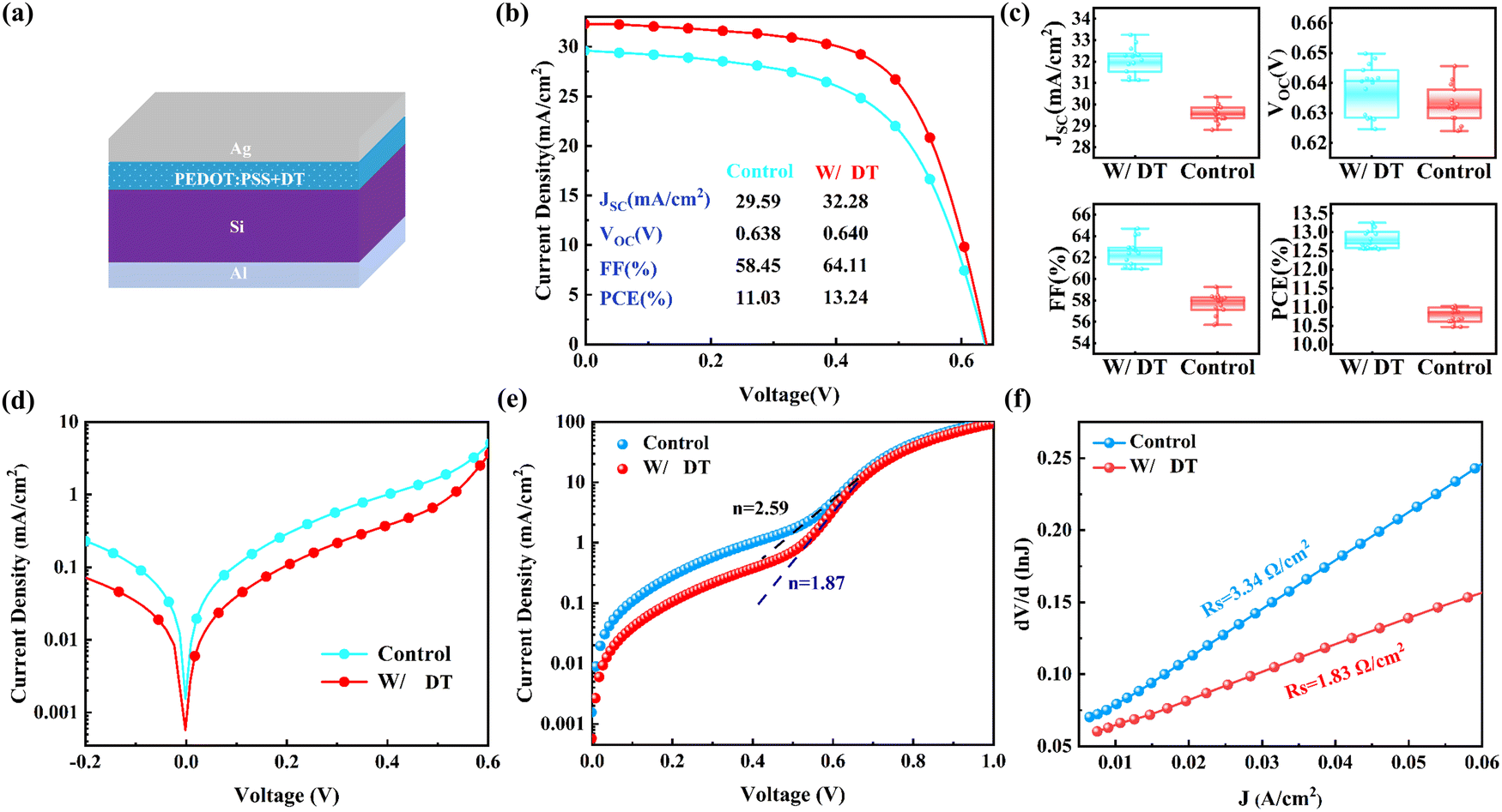 | ||
Fig. 4 (a) Schematic of the devices with DT. (b) J–V curves under 100 mW cm−2 illumination (AM 1.5), (c) statistical plots of the photovoltaic performance and (d) dark J–V curves of the devices with or without DT. (e) Linear fitting and (f) dV/d(ln![[thin space (1/6-em)]](https://www.rsc.org/images/entities/char_2009.gif) J)–J curves calculated from the dark J–V curves of the devices with and without DT. J)–J curves calculated from the dark J–V curves of the devices with and without DT. | ||
To explain the reason for the increase in the photovoltaic characteristics, the J–V curves of the corresponding devices under dark conditions were measured. It can be seen that the DT-added device had a reduced leakage current in Fig. 4d, indicating better charge extraction and collection efficiency, which is thus beneficial for the enhancement of Jsc and FF.7,40 The dark J–V curves of devices with different concentrations of DT are shown in Fig. S6 (ESI†). The ideal factor (n) and reverse saturation current density (J0) were calculated from the following formula:

Fig. 5a shows the structure of the colored devices. To adjust the hue of the devices, different thicknesses of DT coating were covered on the top surface of the DT-added devices with the thickness of the PEDOT:PSS + DT films or PEDOT:PSS films fixed at around 100 nm. As shown in Fig. S8 (ESI†), the champion PCE of the control device is 11.03% with a JSC of 29.59 mA cm−2, whereas that of the colored control devices (reference purple devices) dropped to 10.44% with a JSC of 28.57 mA cm−2. The JSC and PCE of the colored device clearly decreased, as the DT coating increases the reflection and diminishes the absorption of incident light. To enhance the photovoltaic performance of the colored devices, DT as additive was also introduced into the PEDOT:PSS film, resulting in the attainment of more efficient colorful DT-added devices. The graph and J–V curves of the colored sample with the PEDOT:PSS + DT films are shown in Fig. 5b, and the related CIE 1931 chromaticity diagram is presented in Fig. 5c. It can be seen that the purple, blue, cyan, green and yellow devices were obtained, with the corresponding CIE 1931 color coordinates, thickness and photoelectric parameters presented in Table 1. Noticeably, the photovoltaic performance of the purple device with added DT was clearly enhanced compared to the reference purple device. It had the thinnest DT coating thickness and lowest optical loss, yielding the highest JSC of 31.13 mA cm−2 and PCE of 12.36%. There are slight differences in the Voc and FF values for the colorful devices. The JSC of 28.40–31.13 mA cm−2 and PCE of 10.94–12.36% for the devices from a purple to yellow color show the significant decline with increasing DT film thickness. Very interestingly, although the champion PCE of the color devices are lower than that (13.24%) of the dark-color DT-added device without coating, it is higher than that (11.03%) of the control device without the added DT and DT coating. In addition, all colorful devices have a relative PCE of over 99% compared to the uncolored control devices. These results demonstrate that such method for obtaining vivid solar cells is practical and has potential for broadening novel applications.
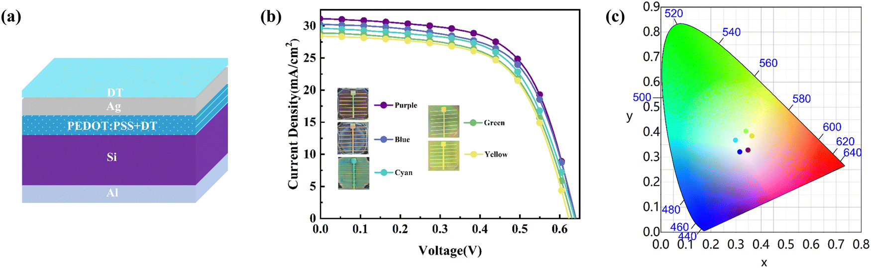 | ||
| Fig. 5 (a) Schematic of the colored devices. (b) J–V curves of the colorful devices under 100 mW cm−2 illumination (AM 1.5). (c) Coordinates of the colored devices in the CIE 1931 chromaticity diagram. | ||
| Colored devices | Thickness of PEDOT:PSS + DT and DT film (nm) | CIE 1931 (x, y) | J SC (mA cm−2) | V OC (mV) | FF (%) | PCE (%) |
|---|---|---|---|---|---|---|
| Purple | 110 | (0.3466, 0.3279) | 31.13 | 0.638 | 62.25 | 12.36 |
| Blue | 120 | (0.3154, 0.3213) | 30.26 | 0.641 | 61.51 | 11.92 |
| Cyan | 160 | (0.2982, 0.3682) | 29.65 | 0.638 | 60.90 | 11.52 |
| Green | 370 | (0.3405, 0.4046) | 28.89 | 0.631 | 60.58 | 11.04 |
| Yellow | 220 | (0.3642, 0.3854) | 28.40 | 0.623 | 61.82 | 10.94 |
3.4 Stability of the devices
Good stability is very critical for increasing the possibility of commercial applications for PEDOT:PSS/Si HSCs. As shown in Fig. 6a and b, there is a slower deterioration in VOC, FF and PCE for the colored devices covered by the DT coating compared to the control device without any DT coating in air at room temperature and relative humidity of 60%. The colored devices retain 70% of its initial PCE after 15 days, while the control device only maintains 20%, suggesting that the DT coating can act as an encapsulating layer of the devices to obtain better stability in air, as DT films are able to effectively avoid the moisture absorption of PEDOT:PSS.23 In addition, extreme aging tests for the devices were conducted by keeping devices directly irradiated by a UV lamp in ambient air at room temperature and relative humidity of 60%. As shown in Fig. S9 (ESI†), under UV irradiation, devices covered with the DT coating can absorb UV and emit green light, while those without the DT coverage did not emit light. Fig. 6c and d show that the PCE and FF of the devices without the DT coating quickly drop to 36% and 46%, respectively, under strong UV illumination in ambient air for 11 hours. Meanwhile, when kept only in ambient air for 1 day (without UV illumination), the PCE and FF of the devices without the DT coating only decreased to 72% and 85%, respectively, as shown in Fig. 6a and b. This finding shows that UV light can further accelerate the degradation rate of the photovoltaic performance of the devices. Interestingly, the device covered by a DT coating exhibits only 16% PCE degradation under intense UV radiation for 11 hours, while the PCE degradation of the control device is higher by 64%. Meanwhile, after UV exposure, the device coated with DT shows slower decline trends with the VOC and FF compared to the device not coated with DT. These results demonstrate that the DT-coated devices have superior stability due to the UV absorption of the DT films. | ||
| Fig. 6 (a) Normalized PCE and (b) photovoltaic parameter degradation of the devices in air. (c) Normalized PCE and (d) photovoltaic parameter degradation of the devices in air and under UV illumination. | ||
To investigate the influence of UV radiation on the stability, PEDOT:PSS films were kept under a UV lamp in the glove box for 11 hours. The AFM measurements show significant changes in the morphology, phase and RMS for the PEDOT:PSS film after UV illumination. Compared to Fig. S3a and b (ESI†), the morphology and phase images in Fig. 7a and b show that the better fiber-like interconnection of the conductive PEDOT chains were broken, and the apparently clustered PEDOT was randomly surrounded by PSS when the PEDOT:PSS film was illuminated by UV light. Moreover, the RMS was significantly increased from 2.68 nm (Fig. 3a) to 3.93 nm (Fig. 7c) with nearly 50% growth rate, suggesting the worse continuity of the PEDOT:PSS film after UV illumination. Fig. 7d–f shows that although the PEDOT chains were also damaged after UV irradiation, the PEDOT:PSS film with the DT coating still maintained a better linear PEDOT structure that was less surrounded by PSS. Furthermore, the PEDOT:PSS film with the DT coating exhibited a lower RMS (3.42 nm) than that without the DT coating. The results demonstrated that the DT coating can reduce the damage to the morphology of the PEDOT:PSS films caused by UV irradiation.
 | ||
| Fig. 7 (a) AFM morphology, (b) phase images and (c) RMS of the PEDOT:PSS film under UV illumination. (d) AFM morphology, (e) phase images and (f) RMS of the PEDOT:PSS film with DT coating under UV illumination. | ||
Fig. 8a and b show the O 1s and C 1s XPS spectra of the fresh as-prepared PEDOT:PSS film, and one with or without DT coating illuminated by a UV lamp. For the O 1s spectra, there are two peaks at 533 eV and 531 eV corresponding to the C–O of PEDOT and SO of PSS, respectively.45 After UV illumination, the O 1s peak area ratio between PSS and PEDOT increased (Fig. 8a), indicating that the C–O structures in PEDOT decreased. Meanwhile, the peak value of C–O of PEDOT at 286.2 eV in the C 1s XPS band (Fig. 8b) also decreased, further demonstrating the breaking of the C–O bonds in PEDOT.46 These changes of the C–O structures confirmed that the conjugated structure of PEDOT was disrupted.23 Meanwhile, it can be seen from Fig. 8a and b that there was less cleavage of the C–O bonds in PEDOT for the PEDOT:PSS films with the DT coating. To further analyze the structure of PEDOT after UV illumination, Raman spectra were obtained and are shown in Fig. 8c. The Raman spectrum of the fresh as-prepared PEDOT:PSS film presents a main peak at 1426 cm−1. However, a blue shift to 1435 cm−1 was observed after UV irradiation, which indicated an increasingly coiled conformation and cluster of PEDOT groups in the PEDOT:PSS films.47,48
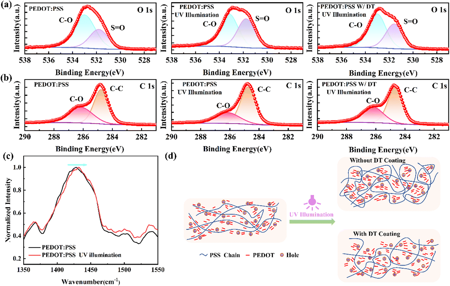 | ||
| Fig. 8 XPS spectra in the (a) O 1s and (b) C 1s regions of the fresh as-prepared PEDOT:PSS film, and the PEDOT:PSS film with and without the DT coating illuminated by a UV lamp. (c) Normalized Raman spectra of the fresh as-prepared PEDOT:PSS film and PEDOT:PSS film illuminated by a UV lamp. (d) Schematic of the changes in the PEDOT:PSS film with or without the DT coating after UV illumination. | ||
Based on the above analysis via AFM, XPS and Raman spectroscopy, the effect of the UV irradiation on the PEDOT:PSS films is exhibited schematically in Fig. 8d. For the PEDOT:PSS films after UV irradiation, the disrupted linear structure of PEDOT damaged the charge transfer channel. Meanwhile, the conductive PEDOT was more tightly surrounded by the insulating PSS, limiting the charge transfer and hopping. These adverse changes caused a decrease in the conductivity of the PEDOT:PSS films, leading to worse stability in the devices. However, for the PEDOT:PSS films with the DT coating, the negative impact of UV illumination on the PEDOT:PSS films is relatively weak; namely, there is less disruption to the structure and morphology. The results illustrate that the DT coating can effectively enhance the stability of the structure and morphology of PEDOT:PSS films, thus leading to improved stability of the DT-coated color devices under UV illumination.
For planar PEDOT:PSS/Si HSCs, there have been many reports on other materials that served as the additive or coating to achieve certain goals, such as high PCE, color tunability, and excellent stability. Here, we have summarized the representative research in Table 2. It can be seen that only DT can serve as both additive and coating, while achieving improved PCE, color tuning, and enhanced stability in the air and under UV illumination. Moreover, the preparation of efficient, stable and colored devices by using the DT additive and coating has the advantages of a low-cost and simple process, as a simple spin-coating step, cheap materials and inexpensive equipment are used during the preparation process.
| Material | Role in devices | Method | Device structure | Device color | Stability | Improved PCE | Ref. |
|---|---|---|---|---|---|---|---|
| DT | Additive Coating | Spin-coating | Uncolored device: Al/Si/PEDOT:PSS + DT/Ag | Multi-color | Enhanced stability in air and under extreme UV irradiation | Uncolored device: 13.24% | Our work |
| Colored device: Al/Si/PEDOT:PSS + DT/Ag/DT | Colored device: 12.36% | ||||||
| Vanadium pentoxide (V2O5) | Additive | Spin-coating | Al/Si/PEDOT:PSS + V2O5/Ag | Dark | — | 15.17% | 40 |
| Waterborne acrylic resin (WA) | Additive | Spin-coating | Al/Si/PEDOT:PSS + WA/Ag | Dark | Enhanced stability in air and under extreme UV irradiation | 13.37% | 20 |
| 2,3,5,6-Tetrafluoro-7,7,8,8-tetracyanoquinodimethane (F4TCNQ) | Additive | Spin-coating | Al/Si/PEDOT:PSS + F4TCNQ/Ag | Dark | — | 13.23% | 35 |
| CuI | Coating | Vacuum deposition | InGa/Si/SiOX/PEDOT:PSS/Ag/CuI | Dark | Enhanced stability in air | 14.30% | 24 |
| GO | Coating | Spin-coating | InGa/Si/PEDOT:PSS/GO/Ag | Dark | Enhanced stability in air | 13.76% | 25 |
| MoO3 | Additive | Spin-coating | Al/PCBM/Si/PEDOT:PSS + MoO3/Ag | Multi-color | — | 13.23% | 6 |
4. Conclusions
In summary, we have demonstrated an effective approach to not only design colored PEDOT:PSS/Si HSCs and improve its long-term stability by using a liquid crystal molecule DT coating, but also deliver high-performance devices by adding DT into the PEDOT:PSS films. After mixing the DT (1.2 mg mL−1), the experimental results show that the conductivity of the PEDOT:PSS films was enhanced due to changes in the structure and surface morphology. The best PCE of the DT-added device was then boosted to 13.24% because of the lower recombination, better junction quality and accelerating charge transport. Notably, when the DT coating was added to the top surface of the DT-added devices, colored devices with 5 colors (purple, blue, cyan, green, yellow) can be achieved. The PCE values of these devices vary from 10.94% (yellow) to 12.36% (purple), exceeding 99% relative PCE of the uncolored control devices. In addition, we discovered the mechanism for the stability damaged by UV radiation; namely, UV light can cause an increase in RMS, aggregation of PEDOT chains and disrupted conjugation of PEDOT, leading to a decline in the performance of the devices. However, the DT coating covered on the surface of the device can effectively avoid the damage from UV irradiation by absorbing UV light and isolating air to achieve excellent device stability. These results reported here offer a practical, economical and convenient method to fabricate efficient, stable and colorful PEDOT:PSS/Si HSCs, and create possibilities of application for colored photovoltaics in building-integrated photovoltaics.Author contributions
Zheng Zhou: writing – original draft, investigation. Shibo Chen: investigation. Yingming Shen: writing – original draft. Juan Wang: methodology. Guijun Zhang: methodology. Yang Shi: formal analysis. Haixia Wu: formal analysis. Jingjing Luo: formal analysis. Xiaohong Cheng: supervision. Yu Yang: supervision, conceptualization.Data availability
The data supporting this article have been included as part of the ESI.†Conflicts of interest
The authors declare that they have no conflict of interest.Acknowledgements
This work was supported by the Funds for Leading Local Scientific-Technological Development by the Central Government (grant no. 202307AB110010), the Department of Science and Technology of Yunnan Province 2025 Annual Basic Research Special-Major Program (grant no. 202501BC070004), the Yunling Scholars Fund of Yunnan Province Xing Dian Talents Program (grant no. KC194317) and Science and Technology Program of Yunnan Precious Metals Laboratory - Basic Research Program (grant no. YPML-20240502007). We also gratefully acknowledge the Advanced Analysis and Measurement Center of Yunnan University.References
- B. Q. Sun, M. W. Shao and S. T. Lee, Adv. Mater., 2016, 28, 10539–10547 CAS.
- X. X. Wang, Z. L. Liu, Z. H. Yang, J. He, X. Yang, T. B. Yu, P. Q. Gao and J. C. Ye, Small, 2018, 14, 1704493 Search PubMed.
- K. Ding, X. Zhang, L. Ning, Z. Shao, P. Xiao, A. Ho-Baillie, X. Zhang and J. Jie, Nano Energy, 2018, 46, 257–265 CAS.
- H. Eggers, S. Gharibzadeh, S. Koch, F. Schackmar, D. B. Ritzer, T. Abzieher, B. S. Richards, C. Erban and U. W. Paetzold, Sol. RRL, 2022, 6, 2100897 Search PubMed.
- J. H. Noh, S. H. Im, J. H. Heo, T. N. Mandal and S. I. Seok, Nano Lett., 2013, 13, 1764–1769 Search PubMed.
- L.-M. Yu, J.-X. Man, T. Chen, D. Luo, J. Wang, H. Yang, Y.-B. Zhao, H. Wang, Y. Yang and Z.-H. Lu, Nano Energy, 2021, 85, 105937 Search PubMed.
- J. Wang, W. Zhou, Q. Wei, G. Liu, X. Yuan, H. Pen, G. Zhang, R. Wang, C. Wang and Y. Yang, Adv. Mater. Interfaces, 2023, 10, 2300187 CAS.
- J. Y. Kim, J. H. Jung, D. E. Lee and J. Joo, Synth. Met., 2002, 126, 311–316 CAS.
- J. Ouyang, Q. Xu, C.-W. Chu, Y. Yang, G. Li and J. Shinar, Polymer, 2004, 45, 8443–8450 CrossRef CAS.
- D. Alemu, H. Y. Wei, K. C. Ho and C. W. Chu, Energy Environ. Sci., 2012, 5, 9662–9671 Search PubMed.
- D.-Y. Khang, J. Phys. D: Appl. Phys., 2019, 52, 503002 Search PubMed.
- Q. Liu, I. Khatri, R. Ishikawa, K. Ueno and H. Shirai, Appl. Phys. Lett., 2013, 102, 183503 CrossRef.
- X. Fang, T. Song, R. Liu and B. Sun, J. Phys. Chem. C, 2014, 118, 20238–20245 CrossRef CAS.
- Z. H. Xia, T. Song, J. Sun, S. T. Lee and B. Q. Sun, Appl. Phys. Lett., 2014, 105, 241110 Search PubMed.
- J. P. Thomas, M. A. Rahman, S. Srivastava, J. S. Kang, D. McGillivray, M. Abd-Ellah, N. F. Heinig and K. T. Leung, ACS Nano, 2018, 12, 9495–9503 Search PubMed.
- Y. H. Kim, C. Sachse, M. L. Machala, C. May, L. Müller-Meskamp and K. Leo, Adv. Funct. Mater., 2011, 21, 1076–1081 Search PubMed.
- Z. Liu, Z. Yang, S. Wu, J. Zhu, W. Guo, J. Sheng, J. Ye and Y. Cui, ACS Nano, 2017, 11, 12687–12695 Search PubMed.
- S. Jäckle, M. Liebhaber, J. Niederhausen, M. Büchele, R. Félix, R. G. Wilks, M. Bär, K. Lips and S. Christiansen, ACS Appl. Mater. Interfaces, 2016, 8, 8841–8848 CrossRef PubMed.
- J. Huang, K. X. Wang, J. J. Chang, Y. Y. Jiang, Q. S. Xiao and Y. Li, J. Mater. Chem. A, 2017, 5, 13817–13822 Search PubMed.
- L. Jiang, Z. Zhou, G. J. Zhang, C. G. Li, Q. S. Feng, Q. W. Wei, J. Y. Li, H. X. Wu, Y. Shi, J. Wang and Y. Yang, ACS Appl. Energy Mater., 2024, 7, 3927–3936 CrossRef CAS.
- G. Zhang, H. Peng, Q. Wei, Z. Zhou, H. Wu, J. Luo, J. Wang, X. Wen and Y. Yang, ACS Omega, 2024, 9, 15040–15051 CrossRef CAS PubMed.
- Q. M. Liu, R. Ishikawa, S. Funada, T. Ohki, K. Ueno and H. Shirai, Adv. Energy Mater., 2015, 5, 1500744 Search PubMed.
- J. He, P. Q. Gao, Z. H. Yang, J. Yu, W. Yu, Y. Zhang, J. Sheng, J. C. Ye, J. C. Amine and Y. Cui, Adv. Mater., 2017, 29, 1606321 CrossRef PubMed.
- J. He, P. Gao, Z. Ling, L. Ding, Z. Yang, J. Ye and Y. Cui, ACS Nano, 2016, 10, 11525–11531 Search PubMed.
- M. Lv, Z. Wang, C. Jiao, Y. Zhao, L. Jin, Y. Fu, Q. Liu and D. He, ACS Appl. Energy Mater., 2021, 4, 13279–13287 Search PubMed.
- E. Toto, S. Botti, S. Laurenzi and M. Gabriella Santonicola, Appl. Surf. Sci., 2020, 513, 145839 CAS.
- A. Vázquez-López, M. García-Carrión, D. Maestre, S. Z. Karazhanov, E. S. Marstein, B. Méndez and A. Cremades, Polym. Degrad. Stab., 2023, 209, 110272 Search PubMed.
- S. Chen, T. Ma, X. Du, M. Mo, Z. Wang and X. Cheng, J. Mol. Liq., 2023, 373, 121239 CAS.
- X. F. Liao, Q. N. He, G. Q. Zhou, X. X. Xia, P. P. Zhu, Z. Xing, H. M. Zhu, Z. Y. Yao, X. H. Lu and Y. W. Chen, Chem. Mater., 2021, 33, 430–440 CAS.
- Q. Lai, R. Zhuang, K. Zhang, T. Wu, L. Xie, R. Zhao, L. Yang, Y. Wang and Y. Hua, Angew. Chem., Int. Ed., 2023, 62, e202305670 Search PubMed.
- Q. Ul Ain, J. X. Xia, H. Kanda, I. R. Alwani, X. X. Gao, H. U. Rehman, G. Shao, V. Jankauskas, K. Rakstys, A. A. Khan and M. K. Nazeeruddin, Sol. RRL, 2023, 7, 2200920 Search PubMed.
- Y. Jiang, B. Luo, F. Jiang, F. Jiang, C. Fuentes-Hernandez, T. Liu, L. Mao, S. Xiong, Z. Li, T. Wang, B. Kippelen and Y. Zhou, Nano Lett., 2016, 16, 7829–7835 CAS.
- J. He, Y. Wan, P. Gao, J. Tang and J. Ye, Adv. Funct. Mater., 2018, 28, 1802192 Search PubMed.
- Y. Zhao, L. Zhang, M. Lv, C. Jiao, P. Cheng, Y. Fu, J. Li, Q. Liu and D. He, ACS Appl. Mater. Interfaces, 2021, 13, 31171–31179 CAS.
- C. Yang, Z. Luo, W. Ma, S. Li, G. Lv, K. Fu, K. Liu, H. Li, H. Sun and X. Chen, J. Phys. Chem. C, 2023, 127, 7974–7986 CAS.
- S. Garreau, J. L. Duvail and G. Louarn, Synth. Met., 2001, 125, 325–329 CrossRef.
- J. Hossain, Q. Liu, T. Miura, K. Kasahara, D. Harada, R. Ishikawa, K. Ueno and H. Shirai, ACS Appl. Mater. Interfaces, 2016, 8, 31926–31934 Search PubMed.
- Y. Jiang, T. Liu and Y. Zhou, Adv. Funct. Mater., 2020, 30, 2006213 CrossRef CAS.
- Y. J. Xia, K. Sun and J. Y. Ouyang, Energy Environ. Sci., 2012, 5, 5325–5332 Search PubMed.
- Z. Luo, C. Yang, X. Chen, W. Ma, S. Li and K. Fu, J Materiomics., 2023, 9, 438–446 CrossRef.
- X. Mu, X. Yu, D. Xu, X. Shen, Z. Xia, H. He, H. Zhu, J. Xie, B. Sun and D. Yang, Nano Energy, 2015, 16, 54–61 Search PubMed.
- S. K. Cheung and N. W. Cheung, Appl. Phys. Lett., 1986, 49, 85–87 Search PubMed.
- C. He, C. M. Zhong, H. B. Wu, R. Q. Yang, W. Yang, F. Huang, G. C. Bazan and Y. Cao, J. Mater. Chem., 2010, 20, 2617–2622 RSC.
- R. K. Sharma, A. Srivastava, P. Kumari, D. Sharma, J. S. Tawale, V. V. Agrawal, B. P. Singh, P. Prathap and S. K. Srivastava, Surf. Interfaces, 2023, 36, 102577 Search PubMed.
- H. Yan and H. Okuzaki, Synth. Met., 2009, 159, 2225–2228 CrossRef CAS.
- N. M. Mackie, D. G. Castner and E. R. Fisher, Langmuir, 1998, 14, 1227–1235 CrossRef CAS.
- X. Crispin, S. Marciniak, W. Osikowicz, G. Zotti, A. W. D. Van der Gon, F. Louwet, M. Fahlman, L. Groenendaal, F. De Schryver and W. R. Salaneck, J. Polym. Sci., Part B:Polym. Phys., 2003, 41, 2561–2583 CrossRef CAS.
- S. Kondratenko, V. Lysenko, Y. V. Gomeniuk, O. Kondratenko, Y. Kozyrev, O. Selyshchev, V. Dzhagan and D. R. T. Zahn, ACS Appl. Energy Mater., 2019, 2, 5983–5991 CrossRef CAS.
Footnote |
| † Electronic supplementary information (ESI) available. See DOI: https://doi.org/10.1039/d5ma00007f |
| This journal is © The Royal Society of Chemistry 2025 |