DOI:
10.1039/D4MA01280A
(Paper)
Mater. Adv., 2025,
6, 1520-1539
Achieving 27.20% efficiency for a lead-free double perovskite solar cell with all inorganic Cs2BiAgI6 using AZO UTL as a passivation layer†
Received
26th December 2024
, Accepted 20th January 2025
First published on 20th January 2025
Abstract
A major challenge in the commercialization of perovskite solar cells (PSCs) is the presence of toxic metals, like lead, in their composition. Compared with conventional lead halide perovskites, double halide perovskites have garnered significant interest owing to their reduced toxicity, adjustable bandgap, structural flexibility, and enhanced stability. This study focuses on evaluating a lead-free Cs2BiAgI6-double perovskite solar cell (DPSC) using a one-dimensional solar cell capacitance simulator (SCAPS-1D) with a bilayer ZnO/AZO electron transport layer (ETL) and ZnO ETL, along with various hole transport layers (HTLs) for the first time. The selected HTLs included CBTS, Cu2O, CuAlO2, CZTS, CuSCN, spiro-OMeTAD, MoO3, and V2O5. Various factors, such as energy band alignment, recombination and generation rates, absorber thickness, defect and doping densities for all layers, energy levels of ETLs and HTL, interfacial defect densities, back metal contact, and operating temperature, were examined for improving the performance of DPSC. This study was aimed at enhancing the efficiency and deepening our understanding of the electron transport mechanisms in Cs2BiAgI6-DPSCs. The research findings suggested that V2O5 and ZnO/AZO were the most suitable materials for the HTL and ETL, respectively, among the various options considered. Therefore, we utilized ITO/ZnO/AZO/Cs2BiAgI6/V2O5/Au as the required DPSC. To boost the performance of the DPSC, electron–hole pair handling at the ETL/perovskite interface was optimized by adding a 10 nm AZO UTL, thereby enhancing the ZnO/double perovskite interface properties. The bilayer structure of ZnO/AZO offered advantages such as efficient electron extraction and minimal interfacial recombination owing to its enhanced energy level alignment and defect passivation. After optimizing these parameters, the system with the ZnO/AZO bilayer ETL achieved an efficiency of 27.20%, along with a Voc of 1.3221 V, Jsc of 23.84 mA cm−2, and FF of 86.28%. Thus, this work presents a straightforward and promising approach for fabricating photovoltaic devices, particularly for various types of double perovskites, with favorable charge transport layers and recombination properties. Furthermore, these findings offer theoretical guidance to improve the efficiency of Cs2BiAgI6-based photovoltaic solar cells (DPSCs) and facilitate the widespread adoption of eco-friendly and stable perovskites.
1. Introduction
To meet the energy demands of daily life, we use fossil fuels, such as natural gas and coal, which are harmful to society and the environment.1,2 Hence, the focus of global research is shifted to the development of alternative energy sources and sustainable energy options that address both economic and environmental concerns. Solar cells are a key renewable energy source, especially perovskite ones, which have attained a significant increase in efficiency from 3.8% to 26.1% since 2009.1,2 The ABX3 formula of perovskite solar cells (PSCs) has a monovalent cation (MA+ = CH3NH3+, FA+ = H2NCHNH2+, and Cs+) as A, a divalent metal cation (lead (Pb2+), tin (Sn2+), titanium (Ti2+), bismuth (Bi2+), and silver (Ag2+)) as B, and a halogen anion (Cl−, Br−, and I−) as X. Lead–halide and organic–inorganic hybrid PSCs have gained attention owing to their high power conversion efficiency (PCE) of 26.1%, which is comparable to top silicon solar cells.3–5 Despite this remarkable efficiency of PSCs, the presence of toxic lead materials and volatile organic cations in their composition hinders their widespread application.6–11 Organic–inorganic PSCs are unstable owing to the presence of oxygen, moisture, and heat generated by organic cations.12 Moreover, lead-based perovskites are very toxic and pose health risks.13–15
The demand for non-toxic PSCs has led to the research on lead-free materials. To replace lead-based perovskites, Sn2+ and Ge2+ (germanium) were used instead of Pb2+ in previous studies. However, Sn2+ and Ge2+ in lead-free PSCs had limited stability owing to oxidation.16 Pb2+ were also replaced with non-toxic Bi3+ ions, which are isoelectronic and stable.17 Bismuth PSCs showed longer charge carrier diffusion owing to their reduced trap densities.18 Introducing Bi3+ in A1+B2+X3 resulted in optoelectronic properties that were worse than those of lead perovskites.19,20 To recover from these inferior characteristics, Bi3+ anion was added to an elpasolite structure or a double perovskite structure.21 Elpasolite structure has the formula A2B1+B3+X6, where A represents a monovalent cation, X represents a halide anion, B1+ represents an inorganic cation, and B3+ represents an organic or inorganic cation. According to recent investigations, double perovskites incorporating Bi3+ and Ag1+ ions exhibit considerable promise for application in photovoltaic technologies because of their advantageous bandgaps, comparable charge carrier effective masses, exceptional photoluminescence lifetimes, extended carrier recombination lifetimes, and robust stabilities.22–27 McClure et al. have stated that Cs2AgBiBr6 and Cs2AgBiCl6 show a noticeable bandgap and exhibit higher stability than MAPbX3.21 However, Cs2AgBiBr6 and Cs2AgBiCl6 exhibit low efficacy owing to their high charge carrier effective masses, restricted charge carrier transport capabilities, and substantial band gap,28–30 making them unsuitable for integration into solar cells. The absorber Cs2AgBiI6 exhibits a band gap of 1.12 eV, excellent light absorption capability and enhanced efficacy compared to Cs2AgBiBr6 and Cs2AgBiCl6, indicating its potential for double perovskite solar cell (DPSC).31,32
The physical properties of a material in a device are key to understanding its state and potential practical applications. Researchers have used density functional theory (DFT) to study material properties, such as halide perovskites. These materials have special properties spotless for optoelectronic and photovoltaic applications.33–35 Hadi et al.36 studied Cs2AgBiBr6 using DFT to explore its properties by inducing disorder in the compound through the creation of an antisite defect in the sublattice; the indirect band gap of Cs2AgBiBr6 was reduced and converted to a direct band gap. This modification enhanced the optical absorption in the visible region, making Cs2AgBiBr6 suitable for solar cell applications.
Here, we conduct a literature review focusing on the ZnO/AZO bilayer structure, exploring its various properties, applications, potential advancements, and efficiency enhancement in the field of PSCs.37
Dong et al.38 reported that ZnO (zinc oxide) nanorods modified with aluminum-doped ZnO (AZO) are utilized in PSCs containing MAPbI3. This modification has demonstrated a beneficial impact on both the Voc (open-circuit voltage) and the PCE. The average PCE is enhanced from 8.5% to 10.07%, with the maximum efficiency reaching 10.7%. Tseng et al.39 reported that Al doping proved to be effective in altering the physicochemical characteristics of ZnO to enhance its performance. A high-quality, fully coated thin film of AZO on an ITO (indium tin oxide) substrate was successfully fabricated using a sputtering technique. When compared to a cell utilizing ZnO, a perovskite cell incorporating AZO as the ETL exhibits superior stability. The most efficient PSC based on AZO achieves a PCE of 17.6% for the ZnO ETL-based PSC. Wu et al.40 reported that the ZnO/perovskite interface has several drawbacks, including the decomposition of MAPbI3 and misaligned energy levels. To solve these issues, we suggest a new design using a low-temperature ZnO/AZO bilayer thin film with band alignment as electron transport layers in PSCs. This enhances PSC efficiency. The PCE increases from 12.3% to 16.1% with the incorporation of the AZO thin film. In addition, some researchers have worked experimentally on the performance of PSCs to improve efficiency using ZnO/AZO bilayer.41–44
To the best of our knowledge, for the first time, the evaluation of lead-free Cs2BiAgI6-DPSC using a one-dimensional solar cell capacitance simulator (SCAPS-1D) with bilayer ZnO/AZO ETL and ZnO ETL with various HTLs is carried out and compared. Various HTLs, including CBTS (copper barium thiostannate), Cu2O (copper(I) oxide), CuAlO2 (copper aluminum oxide), CZTS (copper zinc tin sulfide), CuSCN (copper(I) thiocyanate), Spiro-OMeTAD (2,2′,7,7′-tetrakis[N,N-di(4-ethoxyphenyl)amino]-9,9′-spirobifluorene), MoO3 (molybdenum trioxide), and V2O5 (vanadium oxide) are selected. Next, we investigated the impact of various factors to enhance the performance of the DPSC. These factors included the energy band alignment, total recombination and total generation rate, thickness of the absorber, defect and doping densities of all layers, the energy levels of both ETLs and HTL, the interfacial defect densities of both the ETL and HTL sides, the back metal contact, and operating temperature. This study has the potential to enhance efficiency and deepen our understanding of the electron transport mechanism in Cs2BiAgI6-DPSCs. Additionally, simulation work was carried out on the most efficient cells to gain a more comprehensive understanding of the device's electrical properties. Ultimately, it was revealed that these interfacial bilayers significantly enhanced the photovoltaic characteristics and overall performance of the DPSC.
2. Materials and methodology
2.1. Methodology
Various simulation software, such as SCAPS-1D, PC-1D, AMPS-1D, wxAMPS, COMSOL, and Silvaco, are utilized to simulate the device structures and evaluate the photovoltaic performance of different kinds of solar cells.45 In this particular study, SCAPS-1D version-3.3.08, developed by the Department of Electronics and Information Systems (ELIS) at the University of Gent, Belgium, is employed to simulate and model the DPSC with Cs2BiAgI6 as the active layer.46 The simulation process involves using three semiconductor equations: eqn (1) represents the Poisson equation, which establishes the relationship between carrier concentrations and electrostatic potential, while eqn (2) and (3) correspond to the continuity equations for electrons and holes, respectively. These equations enable the analysis of the charge carrier generation and recombination mechanisms in the semiconductor.| |  | (1) |
| |  | (2) |
| |  | (3) |
where ψ denotes electric potential; ξ denotes the electric field; ε denotes the permittivity; q denotes the electronic charge; p(x) and n(x) are concentrations of charge carriers; τn,p represents the carrier lifetime, μn,p denotes charge mobilities; NA− and ND+ denote shallow acceptor and shallow donor concentrations, respectively; Dn,p denotes the diffusion coefficient of the charge carrier; Gn or Gp denotes the charge carrier generation rate, and pt(x) denote the defect densities of electrons and holes, respectively. At the (x) and pt(x) equilibrium state, we have the following equation:| |  | (4) |
2.2. Device structure and material parameters
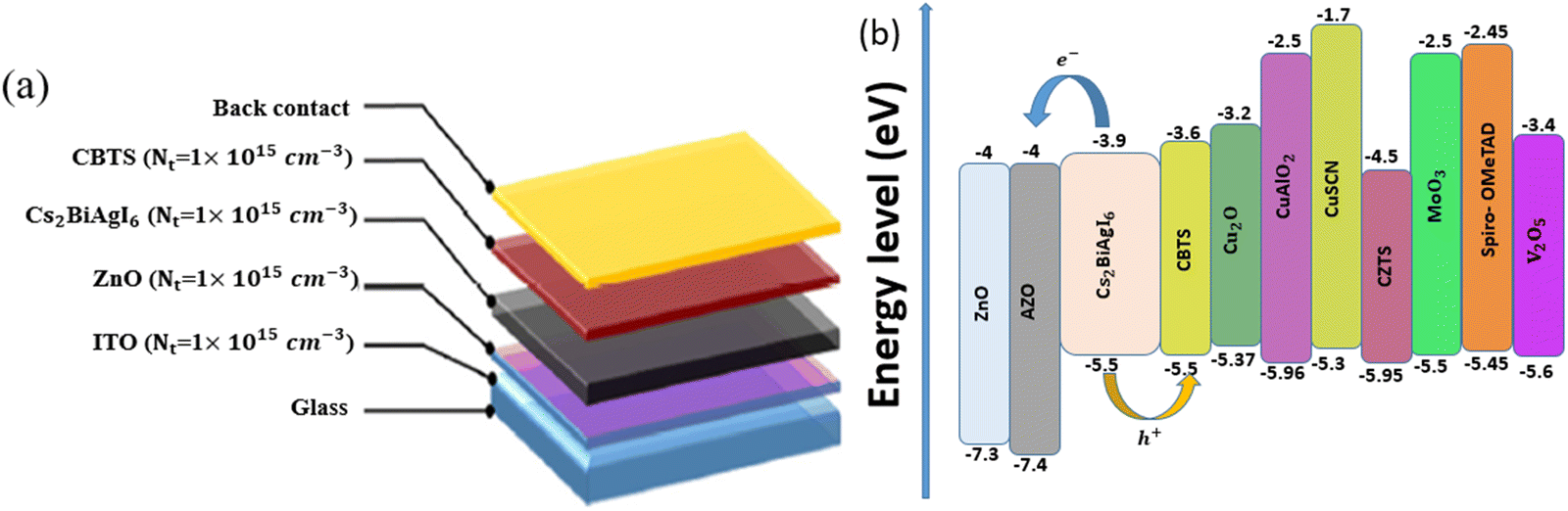
In the formation of a double perovskite solar cell, the Cs2BiAgI6 absorber layer is accompanied by ETL, HTL, and back contact to create the DPSC structure, as it captures photons effectively owing to its double heterostructure, ensuring charge and photon confinement. The performance of various double perovskite solar cell structures (DPSCs) is investigated using SCAPS-1D software, with the ambient temperature set at 300 K and the AM 1.5G sunlight spectrum. Different structures are studied by incorporating two ETLs and eight HTLs, with a gold back contact.
The Cs2BiAgI6-DPSC is composed of multiple layers, including indium tin oxide (ITO), ZnO as ETL, Cs2BiAgI6 as the double perovskite absorbing (DPPVK) layer, and CBTS as HTL.47 Notably, the DPPVK layer, Cs2BiAgI6, exhibits p-type carrier characteristics, with a bulk defect density of 1 × 1015 cm−3. This parameter significantly affects the charge carrier lifetime of electrons and holes, resulting in a value of 100 ns for both. The diffusion lengths of the electron and hole charge carriers, denoted by Ln and Lp, respectively, are measured to be 0.72 μm. For simulation purposes, the DPPVK layer is assumed to have a thickness of 800 nm, as shown in Table 1. The thermal velocity of electrons and holes is confirmed to be 1 × 107 cm s−1. Additionally, the defect energy level is positioned at the center of Eg, following a Gaussian distribution with a characteristic energy of 0.1 eV. These defects are electrically neutral and exhibit optimized capture cross sections for electrons and holes, with a value of 1 × 10⁻¹⁵ cm2. The pre-factor for all the layers, denoted as Aα, is 1 × 10⁵ (cm−1 eV−0.5).47 These values are determined ×using the following equation: α = Aα(hν − Eg)0.5, where hν represents the photon energy. Fig. 1(a) depicts a schematic representation of the Cs2BiAgI6-DPSC device configuration. The defect densities of each layer are specified in parentheses. Fig. 1(b) shows the energy band alignment for two ETLs, eight HTLs, and the DPPVK layer.
Table 1 Material parameters used in the simulation
| Material parameters |
ITO |
ZnO |
Cs2BiAgI6 |
CBTS |
| Thickness (nm) |
500 |
50 |
800 |
100 |
| Energy band gap, Eg (eV) |
3.5 |
3.3 |
1.6 |
1.9 |
| Electronaffinity, χ (eV) |
4 |
4 |
3.9 |
3.6 |
| Relativedielectricpermittivity, εr |
9 |
9 |
6.5 |
5.4 |
| Conduction band effective density of state, NC (cm−3) |
2.2 × 10¹⁸ |
3.7 × 10¹⁸ |
1 × 10¹⁹ |
2.2 × 10¹⁸ |
| Valence band effective density of state, NV (cm−3) |
1.8 × 10¹⁹ |
1.8 × 10¹⁹ |
1 × 10¹⁹ |
1.8 × 10¹⁹ |
| Electronmobility, μn (cm2 V−1 s−1) |
20 |
100 |
2 |
30 |
| Holemobility, μp (cm2 V−1 s−1) |
10 |
25 |
2 |
10 |
| Shallow uniform donor doping density, ND (cm−3) |
1 × 10²¹ |
1 × 10¹⁸ |
0 |
0 |
| Shallow uniform acceptor doping density, NA (cm−3) |
0 |
0 |
1 × 10¹⁵ |
1 × 10¹⁸ |
| Defect density, Nt (cm−3) |
1 × 10¹⁵ |
1 × 10¹⁵ |
1 × 10¹⁵ |
1 × 10¹⁵ |
| Electron thermal velocity, Ve (cm s−1) |
1 × 10⁷ |
1 × 10⁷ |
1 × 10⁷ |
1 × 10⁷ |
| Hole thermal velocity, Vh (cm s−1) |
1 × 10⁷ |
1 × 10⁷ |
1 × 10⁷ |
1 × 10⁷ |
| Ref. |
47
|
47 and 48
|
47
|
47
|
 |
| | Fig. 1 (a) Device structure of the Cs2AgBiI6-DPSC. The defect densities of each layer (Nt) are shown in the parentheses. (b) Energy band alignment of ETLs, HTLs, and the DPPVK layer. | |
The validation of the model is confirmed through a comparison of the results obtained from Hossain et al.47 with our model for the ITO/ZnO/Cs2BiAgI6 (800 nm)/CBTS/Au device. In Table 1, the material parameters for this device are presented. Table 2 shows the interface defect density parameters used in our simulation.
Table 2 Interface defect density parameters47
| Interface parameter |
ZnO/Cs2BiAgI6 |
Cs2BiAgI6/CBTS |
|
σ
n,p: capture cross section for electron and hole; Et: defect energy level; EV: valence band minimum energy; Nt: interface defect density. |
| Defect type |
Neutral |
Neutral |
|
σ
n
(cm2) |
1 × 10⁻¹⁷ |
1 × 10⁻¹⁸ |
|
σ
p
(cm2) |
1 × 10⁻¹⁸ |
1 × 10⁻¹⁹ |
| Distribution of energy |
Single |
Single |
|
E
t–EV |
Above the VB maximum |
Above the VB maximum |
| Energy level w.r.t. reference (eV) |
0.6 |
0.6 |
|
N
t (cm−2) |
1 × 10¹⁰ |
1 × 10¹⁰ |
Fig. 2(a) shows our simulation of the current density–voltage curve of DPSC, ITO/ZnO/Cs2BiAgI6 (800 nm)/CBTS/Au, with the PV output parameters of Voc of 1.0890 V, Jsc of 24.18 mA cm−2, FF of 81.87%, and PCE of 21.56%, and Fig. 2(b) demonstrates the simulation of the EQE curve against the wavelength of the corresponding device. The EQE curve commences from 27.922% at 300 nm and reaches a peak of 99.807% at 360 nm. Then, it remains almost constant up to 600 nm and finally decreases to zero at 780 nm. Additionally, Fig. 2(c) shows the energy band alignment of this device.
 |
| | Fig. 2 Simulation results for the (a) current density–voltage (J–V) curve, (b) external quantum efficiency (EQE) curve, and (c) energy band alignment of the ITO/ZnO/Cs2BiAgI6 (800 nm)/CBTS/Au device.47 | |
Table 3 displays the comparison between the Hossain et al.47 result and our simulated performance parameters of ITO/ZnO/Cs2BiAgI6 (800 nm)/CBTS/Au.
Table 3 Comparison of the results of Hossain et al.47 with our simulation of performance parameters for ITO/ZnO/Cs2BiAgI6 (800 nm)/CBTS/Au
| PV parameters |
V
oc (V) |
J
sc (mA cm−2) |
FF (%) |
PCE (%) |
|
V
oc (open-circuit voltage), Jsc (short-circuit current density), FF (fill factor), and PCE (power conversion efficiency). |
| Hossain et al.47 |
1.085 |
23.76 |
83.78 |
21.59 |
| Simulation |
1.089 |
24.18 |
81.87 |
21.56 |
In this step, we examined AZO ETL and various HTLs to enhance efficiency. It is presumed that the ND (cm−3) and Nt (cm−3) values of AZO ETL are the same as those of ZnO. It is assumed that the thickness of all HTLs is the same as the value of CBTS, and the values of NA (cm−3) and Nt (cm−3) are equal to those of CBTS. Table 4 presents the input material parameters of AZO ETL and different HTLs used in our simulation.
Table 4 Input material parameters of AZO (ETL) and different HTLs used in our simulation
| Material parameters |
ETL |
HTL |
| AZO |
Cu2O |
CuAlO2 |
CuSCN |
CZTS |
MoO3 |
Spiro-OMeTAD |
V2O5 |
| Thickness (nm) |
10 |
100 |
100 |
100 |
100 |
100 |
100 |
100 |
|
E
g (eV) |
3.4 |
2.17 |
3.46 |
3.6 |
1.45 |
3 |
3 |
2.2 |
|
χ (eV) |
4 |
3.2 |
2.5 |
1.7 |
4.5 |
2.5 |
2.45 |
3.4 |
|
ε
r
|
9 |
7.1 |
60 |
10 |
9 |
12.5 |
3 |
10 |
|
N
C (cm−3) |
2 × 10¹⁸ |
2.02 × 10¹⁷ |
2.2 × 10¹⁸ |
2.2 × 10¹⁹ |
2.2 × 10¹⁸ |
2.2 × 10¹⁸ |
2.2 × 10¹⁸ |
9.2 × 10¹⁷ |
|
N
V (cm−3) |
1.8 × 10¹⁹ |
1 × 10¹⁹ |
1.8 × 10¹⁹ |
1.8 × 10¹⁸ |
1.8 × 10¹⁹ |
1.8 × 10¹⁹ |
1.8 × 10¹⁹ |
5 × 10¹⁸ |
|
μ
n
(cm2 V−1 s−1) |
150 |
200 |
2 |
100 |
60 |
25 |
2 × 10⁻⁴ |
3.2 × 10² |
|
μ
p
(cm2 V−1 s−1) |
25 |
80 |
8.6 |
25 |
20 |
100 |
2 × 10⁻⁴ |
4 × 101 |
|
N
D (cm−3) |
1 × 10¹⁸ |
0 |
0 |
0 |
0 |
0 |
0 |
0 |
|
N
A (cm−3) |
0 |
1 × 10¹⁸ |
1 × 10¹⁸ |
1 × 10¹⁸ |
1 × 10¹⁸ |
1 × 10¹⁸ |
1 × 10¹⁸ |
1 × 10¹⁸ |
|
N
t (cm−3) |
1 × 10¹⁵ |
1 × 10¹⁵ |
1 × 10¹⁵ |
1 × 10¹⁵ |
1 × 10¹⁵ |
1 × 10¹⁵ |
1 × 10¹⁵ |
1 × 10¹⁵ |
| Ref. |
49–51
|
52
|
37
|
47
|
53
|
51
|
54 and 55
|
56
|
2.2.1. Influence of various ETLs and HTLs.
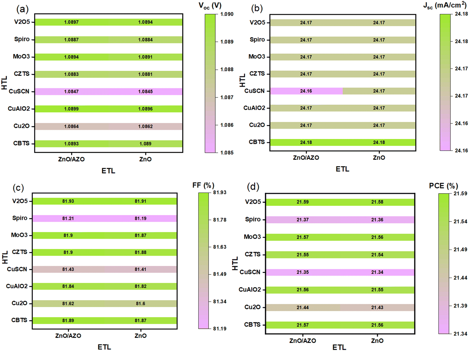
Herein, we explored a DPSC based on Cs2BiAgI6 with an initial configuration using two kinds of ETLs, eight kinds of HTLs, and Au as a back contact. For this study, we used a total of eight HTLs comprising Cu2O, CuSCN, V2O5, Spiro-OMeTAD, MoO3, CuAlO2, CZTS, CBTS, and two ETLs (ZnO and ZnO/AZO) to compare the PV performance for these 16 configurations. During the performance evaluation, the appropriate Cs2BiAgI6 absorber seems to be with HTLs, such as CBTS, CuAlO2, CZTS, MoO3, and V2O5 (Fig. 3). Compared with these HTLs, the performance of Cu2O, CuSCN, and Spiro-OMeTAD was reduced when paired with any of the ETLs. As a p-type layer, the HTL must be thinner than the n-type ETL to avoid recombination and allow for the fast exchange of sufficient charge carriers in the structure. In Fig. 3(a), each of ZnO or ZnO/AZO ETLs and V2O5 HTL showed the highest Voc of 1.894–1.897 V, while CuSCN HTL showed the lowest Voc of 1.0845–1.0847 V. The Jsc of the CBTS HTL was the highest, 24.18 mA cm−2, among all of the studied HTLs, as illustrated in Fig. 3(b). ZnO/AZO ETL and CuSCN HTL showed the lowest Jsc of 24.16 mA cm−2. Fig. 3(c) depicts that the V2O5 HTL had the highest FF of 81.91–81.93%, whereas the Spiro-OMeTAD HTL demonstrated the lowest FF of 81.19–81.21% for all the studied transport layers. Fig. 3(d) illustrates the lowest performance of CuSCN HTL, 21.34–21.35%, while V2O5 HTL illustrates the highest performance of 21.58–21.59%. The V2O5 is characterized by several features, including excellent climate stability and strong optical and electrical properties. The V2O5 film can be fabricated by applying an inexpensive and simple spin-coating technique;57 additionally, it was used as an HTL and interlayer between the perovskite absorber/HTL interface to achieve high solar cell performance.58–61 V2O5 layer has a direct band gap of about 2.20 eV with good thermal stability, optical absorption coefficient, and long-term performance and has been recently put into the high priority production list because of its low environmental impact and low-cost fabrication techniques.62 Furthermore, V2O5 nanoparticles were suitable for the modification of PEDOT:PSS (poly(3,4-ethylenedioxythiophene) polystyrene sulfonate owing to their high stability in acid, good dispersibility in polar solvents, and excellent photoelectric properties, the). Therefore, the conductivity of the resulting anode interfacial layer (AIL) improved. It exhibited different AIL conductivities, where the V2O5:PEDOT:PSS had the highest conductivity owing to the V2O5 nanoparticles filling the pinholes, exposing more PEDOT:PSS chains to the surface core–shell structure.63
 |
| | Fig. 3 Photovoltaic output parameters of (a) Voc (V), (b) Jsc (mA cm−2), (c) FF (%), and (d) PCE (%). Contour mapping plots of the device of ITO/ETLs/Cs2BiAgI6 (800 nm)/HTLs/Au for two ETLs and eight HTLs with different materials. | |
For wiser decision of results, Fig. 3 illustrates the PV output parameters (Voc (V), Jsc (mA cm−2), FF (%), and PCE (%)) of the device of ITO/ETLs/Cs2BiAgI6 (800 nm)/HTLs/Au, for two ETL and eight HTL materials, as contour mapping plots.
Table S1 (ESI†) presents the PV output parameters of 16 devices for two ETLs and eight HTLs of Cs2BiAgI6-DPSC, and ITO/ETLs/Cs2BiAgI6 (800 nm)/HTLs/Au. Fig. S1a–d (ESI†) displays the J–V and EQE curves with the corresponding ETLs (a) and (b) ZnO/AZO and (c) and (d) ZnO for the device of ITO/ETLs/Cs2BiAgI6 (800 nm)/HTLs/Au. The eight HTLs are shown in the inset of Fig. S1a–d (ESI†).
According to Table S1 (ESI†) and Fig. 3, it can be concluded that the Cs2BiAgI6-DPSC with ETL (ZnO/AZO) and HTL (V2O5) has the maximum PCE, attaining 21.59%, together with a Voc of 1.0897 V, Jsc of 24.17 mA cm−2, and FF of 81.93%. We employ an ultra-thin layer of AZO (10 nm) on a ZnO, ITO/ZnO/AZO/Cs2BiAgI6 (800 nm)/V2O5/Au device in our simulation. By incorporating an AZO UTL layer, the extraction of electrons is improved at the interface, resulting in efficient carrier extraction, minimal leakage loss,64 and reduced energy loss.65 Additionally, it enhances the alignment of energy levels, facilitates electron transport, and enhances resistance to recombination.66 A bilayer ETL can be designed to have superior film quality, lower trap density, and decreased charge accumulation at the ETL/perovskite interface in the devices. The bilayer structure also displays a uniform, smooth surface with fewer defects, which enhances charge extraction at the ETL/DPPVK layer junction compared to a single layer.67 This strategy presents a promising and efficient approach for producing cost-effective, high-performance, and reliable planar DPSCs.40
Fig. 4(a) presents the current density–voltage (J–V) curve, and Fig. 4(b) illustrates the external quantum efficiency (EQE) curve of ITO/ZnO/AZO/Cs2BiAgI6 (800 nm)/V2O5/Au device. The EQE curve originates from 27.782% at 300 nm and reaches a peak of 99.711% at 360 nm. Then, it remains constant until 600 nm and finally decreases to zero at 780 nm. Table S2 (ESI†) shows the interfacial defect density parameters of ITO/ZnO/AZO/Cs2BiAgI6 (800 nm)/V2O5/Au device.
 |
| | Fig. 4 (a) J–V curve and (b) EQE curve for ITO/ZnO/AZO/Cs2BiAgI6 (800 nm)/V2O5/Au device. | |
3. Results and discussion
3.1. Energy band alignment
The energy band alignment between the passivation layer and the DPSC plays a crucial role in determining the performance of the DPSCs. The conduction band (CB) alignment between the passivation layer and the DPSC is particularly important for efficient electron extraction from double perovskite material. It is necessary to have a minimal offset between the CB of the passivation layer and the CB of the DPSC to ensure effective electron extraction. However, the valence band (VB) alignment between the passivation layer and the DPSC is important for blocking the movement of holes. A considerable difference in the VBs is required to prevent holes from migrating towards the ETL and causing recombination. Similarly, proper alignment between the valence band of the HTL and the double perovskite material is crucial for facilitating hole separation. Additionally, a significant offset in the conduction bands of the HTL and DPSC is necessary to prevent electron migration towards the HTL and minimize recombination. To achieve optimal band alignment in DPSCs, a minimal offset at the CB and a maximal offset at the VB between the double perovskite and the ETL are essential, enabling electron flow while blocking hole transmission.68 Similarly, minimal VBO (valence band offset) and maximal CBO (conduction band offset) affect HTL and double perovskite characteristics. These offsets enable seamless transmission of holes from the absorber to the HTL while impeding electron mobility. Fig. S2 (ESI†) depicts the energy band alignment of the Cs2BiAgI6-DPSCs, while Table 5 presents the VBO and CBO assessed by the respective layers. The VBO and CBO values are calculated based on the material's electron affinity (χ) and energy band gap (Eg), as follows:| | | VBO = (χCTL + Eg,CTL) − (χDPPVK + Eg,DPPVK). | (6) |
Table 5 CBO and VBO at interfaces
| Interface |
CBO (eV) |
VBO (eV) |
| Double perovskite/ETL |
|
|
| Cs2BiAgI6/ZnO |
−0.1 |
1.8 |
| Double perovskite/passivation |
|
|
| Cs2BiAgI6/AZO |
−0.1 |
1.9 |
| Passivation/ETL |
|
|
| AZO/ZnO |
0 |
0.1 |
| Double perovskite/HTL |
|
|
| Cs2BiAgI6/CBTS |
0.3 |
0 |
| Cs2BiAgI6/Cu2O |
0.7 |
−0.13 |
| Cs2BiAgI6/CuAlO2 |
1.4 |
0.46 |
| Cs2BiAgI6/CuSCN |
2.2 |
−0.2 |
| Cs2BiAgI6/CZTS |
−0.6 |
0.45 |
| Cs2BiAgI6/MoO3 |
1.4 |
0 |
| Cs2BiAgI6/Spiro |
1.45 |
−0.05 |
| Cs2BiAgI6/V2O5 |
0.5 |
0.1 |
The implementation of an interlayer (IL) is noted to modify the arrangement of energy levels within the films and hinder ion migration. The alignment of interface energy levels significantly affects the rate at which electrons are injected, particularly between the DPPVK layer and the ETL. The presence of an energy barrier at the interfaces results in the recombination of charge carriers, thereby restricting the efficiency of charge transfer. Conversely, the lack of an energy barrier across the interface promotes efficient charge transfer and injection, leading to reduced recombination rates. The addition of an AZO IL, which acts as a passivation layer at the interface of the DPPVK layer and the ETL, improves electron transport through the interface and could potentially reduce interface charge recombination.
3.2. Influence of total generation and recombination rate
Owing to the light incident on the double perovskite solar cell, Fig. 5a–d illustrates the generation and recombination rates for different ETLs. Electron transfers from valence to the conduction band, leaving a hole. The release of electrons and holes contributes to carrier generation. The SCAPS-1D software utilizes the incident photon flux Nphot(λ, x) to determine the creation of electron–hole pairs G(λ, x). By analyzing this photon flux at different positions and wavelengths, the value of G(λ, x) can be calculated as follows:| | | G(λ, x) = α(λ, x)·Nphot(λ, x), | (7) |
where α(λ, x) is the absorption coefficient and Nphot(λ, x) is the photon incident number. Recombination is the opposite of generation, involving the pairing and annihilation of electrons and holes in the conduction band. The recombination rate of a solar cell is determined by the lifespan and density of the charge carriers. Initially, electron–hole recombination is reduced owing to defect states in the absorber layer. Subsequently, the creation of energy states affects the electron–hole recombination profile in the structure of the solar cell. Recombination rates alter owing to defects, as shown in Fig. 5b and d.69 Recombination rate in ZnO/AZO is a little smaller than that of ZnO for V2O5, as illustrated in Fig. 5b and d.
 |
| | Fig. 5 Total generation and recombination rate of (a) and (b) ZnO/AZO and (c) and (d) ZnO ETLs. | |
3.3. Influence of the thickness of the double perovskite absorber (DPPVK) layer on the Cs2BiAgI6-DPSC performance
Herein, we determine the optimum parameters for the ITO (500 nm)/ZnO (50 nm)/AZO (10 nm)/Cs2BiAgI6 (800 nm)/V2O5 (100 nm)/Au device. The impact of varying the thickness of the double perovskite absorber (DPPVK) layer on the cell parameters was calculated. The DPPVK layer thickness ranged from 50 to 1000 nm in 20 increments, with the parameters shown in Fig. 6. In Fig. 6(a), the current density–voltage curves for DPPVK layers from 50 to 1000 nm in 20 steps are shown. As depicted in Fig. 6(b), increasing the DPPVK layer thickness from 50 to 1000 nm in 20 steps, up to 650 nm, boosts EQE; after that, it rises slightly. This increase is due to more charge carriers resulting from better light absorption.70Fig. 6(c) illustrates the device's performance parameters in proportion to the thickness of the DPPVK layer changing from 50 to 1000 nm in 20 steps. The thickness of the DPPVK layer significantly influences the quality and performance of the DPSCs.
 |
| | Fig. 6 (a) J–V curve, (b) EQE curve, and (c) performance parameters for different double perovskite absorber layer thicknesses ranging from 50 to 1000 nm in 20 steps. | |
In accordance with Fig. 6(c), the Voc and FF of the DPPVK layer diminish as the thickness of the layer augments. This is because the excitons generated from photon absorption are unable to overcome the barrier potential of the depletion layer, resulting in a higher recombination rate of charge carriers and an increased reverse saturation current, which ultimately leads to a decrease in Voc.
Increasing the thickness of the DPPVK layer also enhances photon absorption, resulting in the production of more excitons, which, in turn, increases the Jsc and the overall PCE of the DPSC.71 However, further increasing the thickness leads to higher series resistance, which introduces more defects and increases the recombination rate, thereby reducing the FF.72,73
Therefore, when determining the optimal absorber thickness, it is crucial to consider all factors, including Voc, Jsc, FF, and PCE. Experimental studies have demonstrated that the performance of DPSCs is heavily influenced by the morphology of the DPPVK layer, which directly affects the photogenerated lifetime and diffusion length.74,75
Fig. 6(c) demonstrates the performance parameters to Cs2BiAgI6 thickness (50–1000 nm in 20 steps). The optimal value occurs at a thickness of 650 nm, with the corresponding PV output parameters of Voc at 1.1005 V, Jsc at 23.78 mA cm−2, FF of 82.78%, and PCE of 21.67%. The Voc decreases from 1.2101 V to 1.0790 V, Jsc increases from 9.85 mA cm−2 to 24.45 mA cm−2, FF decreases from 85.07% to 80.76%, PCE increases from 10.14% to 21.67% at 650 nm, and then decreases to 21.31% at 1000 nm.
3.4. Influence of defect density in the double perovskite absorber (DPPVK) layer on the Cs2BiAgI6-DPSC performance
Various processes involving generation, recombination, and absorption occur within the DPPVK layer, directly affecting the quality of the layer and the defect density.76 The efficiency of Cs2BiAgI6-DPSC is significantly affected by high defect densities in the DPPVK layer. These defects act as recombination centers, accelerating the recombination rate and shortening the lifespan of charge carriers, which ultimately leads to a decrease in device performance. In Cs2BiAgI6-DPSC, Shockley–Read–Hall (SRH) recombination is prevalent, and the trap-assisted SRH recombination model can be utilized to calculate the diffusion length.77 The SRH recombination formula is represented as follows:| |  | (8) |
where RSRH denotes SRH recombination; n and p denote the electron and hole concentration density, respectively; ni denotes intrinsic density; τn,p denotes carrier lifetime; Ei denotes the intrinsic energy level; and Et denotes trap energy level. Thus, we have| |  | (9) |
where σn,p denotes the capture cross section of electrons and holes, υth denotes the thermal velocity of charge carriers and Nt denotes the total bulk defect density of the DPPVK layer of the Cs2BiAgI6-DPSC. Moreover, the diffusion length L and the diffusion coefficient D are as follows:| |  | (10) |
| |  | (11) |
where k, T, q, and μn,p represent Boltzmann's constant, temperature, charge carriers, and carrier mobility, respectively.
The maximum distance that charge carriers can travel is determined by these equations, which are primarily influenced by the lifetimes of the carriers. In principle, the diffusion length of charge carriers depends mainly on their lifetimes. Furthermore, the defects found in the DPPVK layer serve as non-radiative SRH recombination centers.
Fig. 7a and b display the PV parameters against the defect density of the DPPVK layer, Nt,DPPVK, which ranges from 1 × 1013 cm−3 to 1 × 1017 cm−3. As demonstrated in Fig. 7, the optimal value occurs at a defect density of 1 × 1013 cm−3, with corresponding PV output parameters of Voc at 1.321 V, Jsc at 23.83 mA cm−2, FF of 84.50%, and PCE of 26.61%. As depicted in Fig. 7(a), Voc decreases from 1.321 V to 0.8248 V as Nt,DPPVK increases from 1 × 1013 cm−3 to 1 × 1017 cm−3, and Jsc remains fixed at 23.83 mA cm−2 for both 1 × 1013 cm−3 and 1 × 1014 cm−3, and 23.78 mA cm−2 at 1 × 1015 cm−3 and then decreases to 2.10 mA cm−2 at 1 × 1017 cm−3. As illustrated in Fig. 7(b), FF decreases from 84.82% to 58.15% as Nt,DPPVK increases from 1 × 1014 cm−3 to 1 × 1017 cm−3, and the PCE value is 24.39% at 1 × 1014 cm−3 and then decreases to 1.01% at 1 × 1017 cm−3.
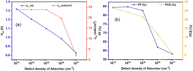 |
| | Fig. 7 (a) Voc and Jsc, and (b) FF and PCE curves for Cs2BiAgI6-DPSC against defect density of absorber. | |
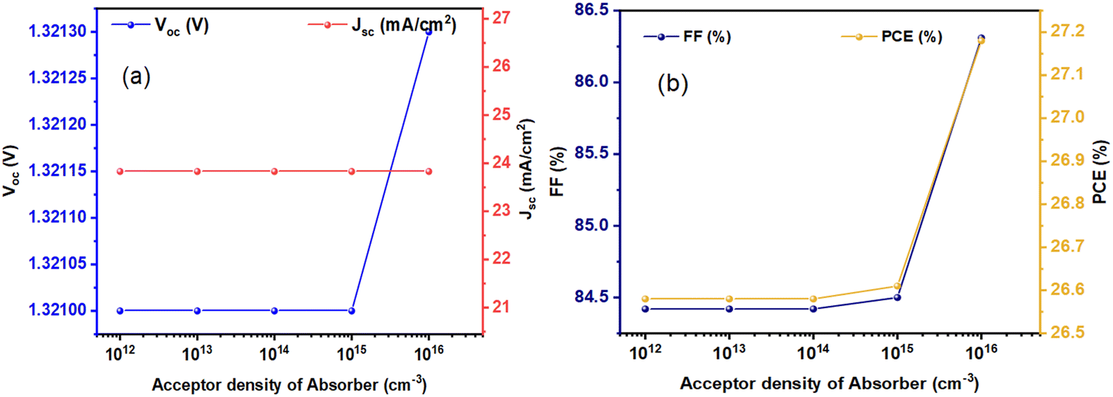
3.5. Influence of acceptor doping concentration in the absorber layer on the Cs2BiAgI6-DPSC performance
The performance of the Cs2BiAgI6-DPSC device is greatly affected by the doping in the DPPVK layer. To explore the effect of acceptor doping density on the Cs2BiAgI6-DPSC performance, we initially model the device performance by adjusting the acceptor doping concentration of the DPPVK layer (NA,DPPVK) from 1 × 1012 cm−3 to 1 × 1016 cm−3, as shown in Fig. 8.
 |
| | Fig. 8 (a) Voc and Jsc, and (b) FF and PCE curves for Cs2BiAgI6-DPSC against acceptor density of absorber. | |
Enhancing the density of dopants can increase the concentration of charge carriers, thus improving the performance of the Cs2BiAgI6-DPSC.78,79 Nevertheless, excessively high levels of doping in the DPPVK layer can lead to reduced device performance, as high doping introduces more traps in the DPPVK layer that affect the mobility of charge carriers and result in increased recombination. Excessive doping densities also influence the semiconductor behavior of Cs2BiAgI6-DPSC, making it more metallic.
Fig. 8a and b show how the values of Voc, Jsc, FF and PCE vary with the acceptor density of the DPPVK layer, which alters from 1 × 1012 cm−3 to 1 × 1016 cm−3. Regarding the acceptor density in the DPPVK layer, the highest efficiency of 27.18% was achieved at an acceptor density of 1 × 1016 cm−3, with the Voc of 1.3213 V, Jsc of 23.83 mA cm−2, and FF of 86.31%. As depicted in Fig. 8(a), Voc is 1.321 V when NA,DPPVK increases from 1 × 1012 cm−3 to 1 × 1015 cm−3 and then increases to 1.3213 V at 1 × 1016 cm−3, and Jsc remains unchanged at 23.83 mA cm−2 from 1 × 1012 cm−3 to 1 × 1016 cm−3. As illustrated in Fig. 8(b), FF is 84.42% when NA,DPPVK increases from 1 × 1012 cm−3 and 1 × 1014 cm−3, marginally increases up to 84.50% at 1 × 1015 cm−3, and then increases to 86.31% at 1 × 1016 cm−3; the PCE value is 26.58% as NA,DPPVK increases from 1 × 1012 cm−3 to 1 × 1014 cm−3, increases to 26.61% at 1 × 1015 cm−3, and increases to 27.18% at 1 × 1016 cm−3.
3.6. Influence of defect density of V2O5-HTL on the Cs2BiAgI6-DPSC performance
Deficiencies in the V2O5 (HTL) film lead to an increase in defect density, causing a higher rate of electron and hole recombination within the film. Consequently, the PCE of Cs2BiAgI6-DPSC decreases.80–82Fig. 9 demonstrates the variation of Voc, Jsc, FF and PCE for defect density of V2O5 and Nt,V2O5, altering from 1 × 1012 cm−3 to 1 × 1018 cm−3. The optimum value increases at 1 × 1017 cm−3, and the PV output parameters of Cs2BiAgI6-DPSC are Voc of 1.3213 V, Jsc of 23.83 mA cm−2, FF of 86.31%, and PCE of 27.18%. As shown in Fig. 9, Voc is 1.3213 V when Nt,V2O5 increases from 1 × 1012 cm−3 to 1 × 1017 cm−3 and then decreases to 1.3203 V at 1 × 1018 cm−3, Jsc is 23.83 mA cm−2 when Nt,V2O5 increases from 1 × 1012 cm−3 to 1 × 1018 cm−3, FF is 86.31% when Nt,V2O5 increases from 1 × 1012 cm−3 to 1 × 1018 cm−3, and PCE value is 27.18% when Nt,V2O5 increases from 1 × 1012 cm−3 to 1 × 1017 cm−3 and then moderately falls to 27.17%.
 |
| | Fig. 9 PV output parameters for Cs2BiAgI6-DPSC against the defect density of V2O5-HTL. | |
3.7. Influence of conduction and valence band offset of V2O5-HTL based on the Cs2BiAgI6-DPSC performance
In the Cs2BiAgI6-DPSC, a comprehensive numerical analysis is conducted with device simulation to understand the device operation mechanism and develop an optimal layer configuration for enhanced efficiency. It is essential to examine the electronic properties of HTL and ETL, such as their electron affinity and band gap, when designing highly efficient solar cells. In this study, we aim to determine the ideal energy levels for efficient Cs2BiAgI6-DPSC design. To achieve this goal, careful selection of CBO1 and VBO1 is necessary. In this study, we investigate how modifying the affinities and band gaps of the V2O5 can lead to optimal values of CBO1 and VBO1. To achieve a higher Voc and reduce recombination, CBO1 or VBO1 must be positive and below 0.3 eV. Negative CBO1 or VBO1 values increase electron and hole accumulation, causing more recombination and lower charge output.83 A positive CBO1 or VBO1 restricts electron movement, while a negative one facilitates it.83 The charge polarity of CBO1 and VBO1 is determined by the barrier height of the charge carriers generated by light, as follows:| | | CBO1 = χHTL − χDPPVK, | (12) |
| | | VBO1 = (χHTL + Eg,HTL) − (χDPPVK + Eg,DPPVK). | (13) |
The electron affinity of HTL changes from 1.5 eV to 2.5 eV, and VBO1 is altered from −0.6 eV to +0.4 eV. Therefore, according to Table S3 (ESI†), when the energy band gap of HTL is concerned, the optimum value increases at 2.1 eV or VBO1 is 0.0 eV, with the PV output parameters obtained as Voc of 1.321 V, Jsc of 23.84 mA cm−2, FF of 86.32%, and PCE of 27.19%. Fig. S3(a) (ESI†) shows the current density-volt xage curve, Fig. S3(b) (ESI†) illustrates the energy band diagram, and the inset of the figures demonstrates the variation of the energy level of V2O5-HTL based versus VBO1 values. Fig. 10a–d illustrates the PV output parameters with a variation of VBO1 between −0.6 eV and +0.4 eV. According to our calculations, there is no change in CBO1, see Table S4 (ESI†).
 |
| | Fig. 10 (a)–(d) PV output parameters with the variation of VBO1 of V2O5/Cs2BiAgI6 between −0.6 eV and +0.4 eV. | |
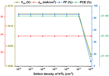
3.8. Influence of defect density of AZO UTL on the Cs2BiAgI6-DPSC performance
Defects in the AZO UTL film lead to more electron–hole recombination. Consequently, the PCE of the Cs2BiAgI6-DPSC decreases.84,85Fig. 11 shows the variation of Voc, Jsc, FF and PCE for defect density of AZO UTL, Nt,AZO, increasing from 1 × 1012 cm−3 to 1 × 1019 cm−3. The optimum value increases at 1 × 1016 cm−3, and the PV output parameters of Cs2BiAgI6-DPSC are Voc of 1.321 V, Jsc of 23.84 mA cm−2, FF of 86.32%, and PCE of 27.19%. As depicted in Fig. 11, Voc is 1.321 V when Nt,AZO increases from 1 × 1012 cm−3 to 1 × 1016 cm−3, slightly decreases to 1.3189 V at 1 × 1018 cm−3, and then increases to 1.3224 V at 1 × 1019 cm−3. Jsc is 23.84 mA cm−2 when Nt,AZO increases from 1 × 1012 cm−3 to 1 × 1018 cm−3 and then decreases to 22.96 mA cm−2 at 1 × 1019 cm−3. FF is 86.32% as Nt,AZO increases from 1 × 1012 cm−3 to 1 × 1017 cm−3, increases to 86.39% at 1 × 1018 cm−3, and then decreases to 81.90% at 1 × 1019 cm−3. PCE value is 27.19% as Nt,AZO increases from 1 × 1012 cm−3 to 1 × 1016 cm−3; to some extent, increases to 27.18% at 1 × 1017 cm−3 and 27.17% at 1 × 1018 cm−3; and then decreases to 24.87% at 1 × 1019 cm−3.
 |
| | Fig. 11 PV output parameters for Cs2BiAgI6-DPSC against the defect density of AZO UTL. | |
3.9. Influence of valence and conduction band offset of AZO UTL on the Cs2BiAgI6-DPSC performance
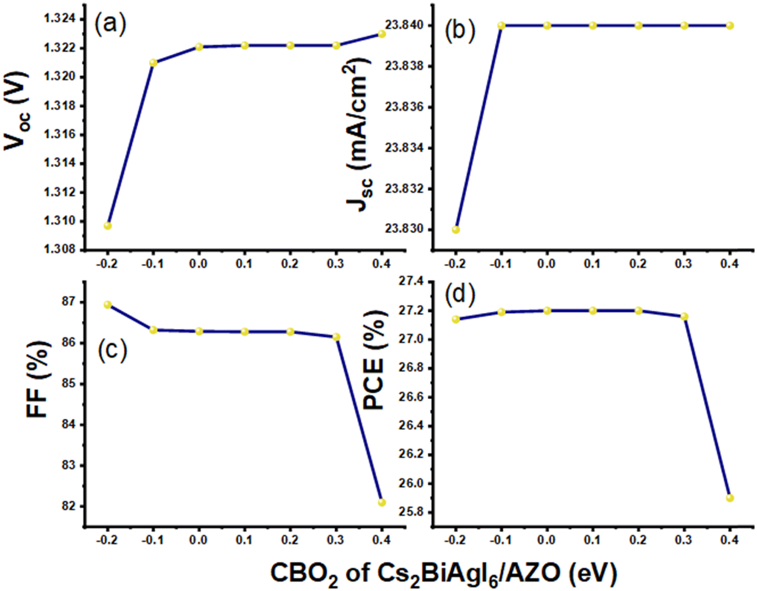
To determine the optimal energy level, it is crucial to carefully select the values of CBO2 and VBO2 for the AZO UTL.83 The barrier heights (CBO2 and VBO2) can be influenced by photo-generated charge carriers, either positive or negative, as follows:| | | CBO2 = χDPPVK − χAZO, | (14) |
| | | VBO2 = (χDPPVK + Eg,DPPVK) − (χAZO + Eg,AZO). | (15) |
Eqn (14) represents the electron affinity of the DPPVK layer (χDPPVK) and the electron affinity of the AZO UTL (χAZO). Eqn (15) presents the band gap energy of the DPPVK layer (Eg,DPPVK) and the band gap energy of the AZO UTL (Eg,AZO).
There is no change in VBO2; see Table S5 (ESI†). In Table S6 (ESI†), PV output parameters are shown, the electron affinity of AZO ranges from 3.5 eV to 4.1 eV, and the CBO2 values change from +0.4 eV to −0.2 eV. Fig. S4(a) (ESI†) shows the plots of current density–voltage curves for different values of CBO2, while Fig. S4(b) (ESI†) illustrates the energy band diagram with various CBO2 values as indicated by different colors. Fig. 12a–d presents the PV output parameters corresponding to several CBO2 values. The optimal value for the DPPVK layer/AZO UTL interface occurs when the electron affinity of AZO UTL is 3.9 eV. The optimum value increases at CBO2 = +0.0 eV because it has better energy alignment and an efficiency of 27.20%, while the PV output parameters of Cs2BiAgI6-DPSC are as follows: Voc of 1.3221 V, Jsc of 23.84 mA cm−2, FF of 86.29%, and PCE of 27.20%.
 |
| | Fig. 12 (a)–(d) PV output parameters with the variation of CBO2 of Cs2BiAgI6/AZO UTL between −0.2 eV and +0.4 eV. | |
3.10. Influence of defect density of ZnO layer on the Cs2BiAgI6-DPSC performance
Because of ZnO layer flaws, the defect density increases, leading to more charge carrier recombination. This leads to a decrease in the PCE of the Cs2BiAgI6-DPSC.86 As depicted in Fig. 13, the defect density of ZnO changes from 1 × 1012 cm−3 to 1 × 1018 cm−3. As illustrated in Fig. 13, Voc is a constant value at 1.3222 V as Nt,ZnO increases from 1 × 1012 cm−3 to 1 × 1017 cm−3, and then marginally decreases to 1.3220 V at 1 × 1018 cm−3. Jsc remains fixed at 23.84 mA cm−2 as Nt,ZnO increases from 1 × 1012 cm−3 to 1 × 1016 cm−3 and slightly decreases to 23.79 mA cm−2 at 1 × 1018 cm−3. FF value is 86.28% when Nt,ZnO increases from 1 × 1012 cm−3 to 1 × 1017 cm−3 and then fairly decreases to 86.27% at 1 × 1018 cm−3. PCE value is 27.20% when Nt,ZnO increases from 1 × 1012 cm−3 to 1 × 1016 cm−3 and then scarcely decreases to 27.14% at 1 × 1018 cm−3.
 |
| | Fig. 13 PV output parameters for Cs2BiAgI6-DPSC against the defect density of the ZnO layer. | |
3.11. Influence of interfacial defect density on the Cs2BiAgI6-DPSC performance
To optimize the efficiency of DPSCs, the quality of the junction plays a crucial role in determining the capabilities of the interface. Our focus in this stage was on adjusting the defect densities at the interface to emphasize the significance of interface quality and recombination rate in actual Cs2BiAgI6-DPSCs. Interactions between double perovskites and transport materials often contain multiple defect states, highlighting the importance of the quality of these interfaces for the PCE of Cs2BiAgI6-DPSC. Notably, the interface defect density near the illuminated side exerts a more pronounced influence on Cs2BiAgI6-DPSC performance compared to the back interface.87 With an increase in these defects, additional trap levels emerge at the interface, consequently elevating the resistance of Cs2BiAgI6-DPSC. The heightened resistances impede the movement of charge carriers, promoting recombination and ultimately diminishing the PCE of DPSC.88
Herein, there are three categories of interface defect densities: the first one is between the HTL and DPPVK layer, the second one is between AZO UTL and DPPVK layer, and the third one is between AZO UTL and ZnO layer.
In Fig. 14(a), it is demonstrated that the optimum value for the interface defect density (Nit) of the HTL/DPPVK layer (Nit changes from 1 × 105 cm−2 to 1 × 1015 cm−2) is 1 × 1010 cm−2; the PV output parameters are as follows: Voc of 1.3221 V, Jsc of 23.84 mA cm−2, FF of 86.28%, and PCE of 27.20%. Regarding HTL/DPPVK interface defect density, Voc is 1.3222 V from 1 × 105 cm−2 to 1 × 109 cm−2 and then decreases to 1.1852 V at 1 × 1015 cm−2. The parameter of Jsc remains constant, 23.84 mA cm−2, as Nit increases from 1 × 105 cm−2 to 1 × 1012 cm−2 and then slightly decreases to 23.72 mA cm−2 at 1 × 1015 cm−2. The FF remains constant at 86.28% from 1 × 105 cm−2 to 1 × 1010 cm−2, increases to 89.36% at 1 × 1014 cm−2, and then decreases to 88.47% at 1 × 1015 cm−2. The PCE remains immutable, 27.20%, from 1 × 105 cm−2 to 1 × 1010 cm−2 and then decreases to 24.88% at 1 × 1015 cm−2.
 |
| | Fig. 14 PV output parameters for interface defect density of (a) V2O5 layer/DPPVK layer, (b) DPPVK layer/AZO UTL, and (c) AZO UTL/ZnO layer of Cs2BiAgI6-DPSC. | |
In Fig. 14(b), the DPPVK layer/AZO UTL interface defect density is changed from 1 × 105 cm−2 to 1 × 1015 cm−2. Voc is fixed at 1.3222 V as Nit increases from 1 × 105 cm−2 to 1 × 109 cm−2 and then decreases to 1.1750 V at 1 × 1015 cm−2. Jsc remains unchanged at 23.84 mA cm−2 as Nit enhances between 1 × 105 cm−2 and 1 × 1012 cm−2. At this point, it marginally dwindles to 23.83 mA cm−2 at both 1 × 1013 cm−2 and 1 × 1014 cm−2 and then decreases to 23.80 mA cm−2 at 1 × 1015 cm−2. The FF value is fixed at 86.28% when Nit increases from 1 × 105 cm−2 to 1 × 1010 cm−2 and subsequently increases to 89.17% at 1 × 1015 cm−2. The PCE value is constant at 27.20% as Nit increases from 1 × 105 cm−2 to 1 × 1010 cm−2 and subsequently decreases to 24.94% at 1 × 1015 cm−2. Concerning the optimal value of this interface defect density, it occurs at 1 × 1010 cm−2, with the following PV output parameters: Voc of 1.3221 V, Jsc of 23.84 mA cm−2, FF of 86.28%, and PCE of 27.20%.
AZO UTL/ZnO layer interface defect density is varied from 1 × 105 cm−2 to 1 × 1015 cm−2. As depicted in Fig. 14(c), Voc remains fixed at 1.3221 V as Nit increases from 1 × 105 cm−2 to 1 × 1015 cm−2. Jsc remains constant at 23.84 mA cm−2 as Nit enhances between 1 × 105 cm−2 and 1 × 1013 cm−2, subsequently slightly decreases to 2383 mA cm−2 at 1 × 1014 cm−2, and then slightly decreases to 23.82 mA cm−2 at 1 × 1014 cm−2. FF remains constant at 86.28% when Nit increases from 1 × 105 cm−2 to 1 × 1015 cm−2. PCE has a fixed value of 27.20% as Nit increases from 1 × 105 cm−2 to 1 × 1013 cm−2; at that point, it decreases to 27.19% at 1 × 1014 cm−2; and 27.18% at 1 × 1015 cm−2. The optimum value of this interface defect density occurs at 1 × 1013 cm−2, and the PV output parameters are as follows: Voc of 1.3221 V, Jsc of 23.84 mA cm−2, FF of 86.28%, and PCE of 27.20%.
In this article, we achieved an efficiency of 27.18% by optimizing the thickness, defect density, and acceptor doping concentration of the Cs2BiAgI6 absorber layer. Here, we want to find the optimum value of the defect density for ETL and HTL. Fig. 9 shows that the optimal defect density for the V2O5-HTL is 1 × 1017 cm−3 (PCE = 27.18%). In Fig. 11, the optimal defect density for the AZO UTL-ETL is 1 × 1016 cm−3 (PCE = 27.19%), while Fig. 13 depicts that the ZnO-ETL layer's optimal defect density is also 1 × cm−3 (PCE = 27.20%). Finally, Fig. 14(c) illustrates the optimal interface defect density for AZO/ZnO as 1 × 1013 cm−2 (PCE = 27.20%).89 The J–V–T (current density vs. voltage for various temperatures) and C–f–T (capacitance vs frequency for various temperatures) measurements can help researchers to determine the defect properties in the perovskite solar cell. Using the J–V–T technique, the J–V curves can be measured at different temperatures. After obtaining the amount of Voc, and plotting it against different temperatures, this linear curve intersection with the Voc-axis gives Et/q (Et: defect energy, q: electron charge); the amount of Et is required in the SCAPS program.90 We can also calculate the C–f curves for different temperatures and C–f–T (thermal admittance analysis, TAS method) using the SCAPS package, which might allow us to calculate the defect density as a function of defect energy Nt(Et) from a set of C(f, T) experimental measurements. More information regarding the parameters (such as Vbi, built-in voltage) could be obtained by referring to the Mott–Schottky analysis, specifically (1/C2vs. V).91,92 Moreover, some other techniques are available for considering the defect properties, such as temperature-dependent space charge limited current (SCLC); deep-level transient spectroscopy (DLTS); Laplace current DLTS (I-DLTS); steady-state photoluminescence (SSPL); time-resolved photoluminescence (TRPL); PL mapping; time-resolved microwave conductivity (TRMC); thermally stimulated current (TSC); transient photocapacitance (TPC); surface photovoltage (SPV) spectroscopy; and time-resolved spectroscopies such as transient absorption and reflection techniques, ultraviolet photoemission spectroscopy (UPS), and scanning tunneling microscopy (STM).93
3.12. Influence of the work function of back metal contact on Cs2BiAgI6-DPSC performance
For the enhanced PCE of Cs2BiAgI6-DPSC, the back metal contact's work function is a critical factor. The value of ϕBC (work function) directly impacts the presence of an appropriate built-in electric field in Cs2BiAgI6-DPSC,94 affecting the electric field that aids in hole transport and collection; thus, ϕBC significantly influences Voc.95 To study the effect of different back electrode ϕBC values on Cs2BiAgI6-DPSC performance, we explored ϕBC ranging from 4.65 eV to 5.9 eV.96 Our findings from simulations are presented in Fig. 15.
 |
| | Fig. 15 (a) J–V curve. Inset of the figure shows C (Carbon), Au (Gold), W (Tungsten), Ni (Nickel), Pd (Palladium), Pt (Platinum), and Se (Selenium) work functions. (b) PV parameters as a bar chart against different work functions of Cs2BiAgI6-DPSCs ranging from 4.65 eV to 5.9 eV. | |
The work function of the back metal contact is a critical parameter for increasing the PCE of the Cs2BiAgI6-DPSC. The value of ϕBC directly affects the presence of an appropriate built-in electric field in the Cs2BiAgI6-DPSC, which in turn influences the transport and collection of holes and ultimately determines the Voc. To investigate the impact of different ϕBC values on the performance of the Cs2BiAgI6-DPSC, we conducted simulations with ϕBC ranging from 4.65 eV to 5.9 eV. The work functions of different materials for back electrodes are as follows: Cu (4.65 eV), Fe (4.81 eV), C (5 eV), Au (5.1 eV), W (5.22 eV), Ni (5.5 eV), Pd (5.6 eV), Pt (5.7 eV), and Se (5.9 eV).96Fig. 15(a) illustrates that at low ϕBC values, the J–V curves display an S-shaped pattern because of the presence of elevated Schottky barriers at the interface between the HTL and back metal contact, leading to an impediment in hole transfer and a decrease in the FF.97,98 Copper (4.65 eV) and iron (4.81 eV) showed this phenomenon in our study. Fig. 15(b) presents the PV parameters of the device ITO/ZnO/AZO/Cs2BiAgI6 (650 nm)/V2O5/BC for different ϕBC values ranging from 4.65 eV to 5.9 eV. The highest efficiency of 27.20% was reached with Ni, Pd, Pt, or Se as the back metal contact, as depicted in Fig. 15(b).
As the work function of the back electrode decreases, the Schottky barrier gradually increases, leading to a higher energy requirement for holes to pass through the barrier. This hinders the transport of holes to the back metal contact,94 which ultimately impedes the effective collection of holes and causes a gentle decrease in Voc, thereby reducing efficiency. By utilizing a back electrode with a high work function, the Fermi level is lowered, facilitating the formation of improved Ohmic contacts.99 Therefore, selecting the appropriate back contact material is crucial for achieving high efficiency in Cs2BiAgI6-DPSCs. It is essential to ensure that the V2O5-HTL and back contact form an ohmic contact at the interface to prevent the formation of a high Schottky barrier. Incorporating a low-cost metal, such as Se, as the back contact, as shown in Fig. 15(b), can significantly enhance the efficiency of Cs2BiAgI6-DPSCs.
3.13. Influence of working temperature on Cs2BiAgI6-DPSC performance
When Cs2BiAgI6-DPSCs are exposed to high temperatures, the performance parameters are affected by the temperature.100 An increase in temperature results in a decrease in Voc and a slight increase in Jsc of Cs2BiAgI6-DPSC.101–103
Cs2BiAgI6-DPSCs are typically used in outdoor settings where temperatures exceed 300 K,104 the outdoor temperature directly affects the performance of Cs2BiAgI6-DPSCs. Investigating temperature's impact on Cs2BiAgI6-DPSC, T ranges from 300 K to 500 K. As temperature increases, Voc decreases, lowering Cs2BiAgI6-DPSC PCE.105 As temperature increases, the defect density in the device increases, and mobility decreases, hurting Cs2BiAgI6-DPSC performance.106 Changes in temperature greatly affect the performance of Cs2BiAgI6-DPSC through its impact on Voc. The relationship between Voc and T can be expressed as follows:105
| |  | (16) |
Eqn (16) reveals an inverse relationship between Voc and T. An increase in T leads to a decrease in Voc and an increase in the diode reverse saturation current.104
The results from Fig. 16 indicate that the performance of the Cs2BiAgI6-DPSCs significantly decreases as the operating temperature increases. This is because RS increases with temperature, which reduces diffusion length and increases recombination rate. Consequently, the FF and efficiency of the Cs2BiAgI6-DPSC decreases.106,107
 |
| | Fig. 16 PV output parameters: (a) Voc, (b) Jsc, (c) FF, and (d) PCE for Cs2BiAgI6-DPSC against temperature. | |
In Fig. 16a–d, the PV output parameters are plotted against various temperatures, which vary from 300 K to 500 K in 11 steps. According to Fig. 16(a), Voc diminishes from 1.3221 V to 1.0501 V. In Fig. 16(b), Jsc increases from 23.84011 mA cm−2 at 300 K to 23.85634 mA cm−2 at 500 K. As depicted in Fig. 16(c), FF decreases from 86.28% to 76.25%. In Fig. 16(d), PCE decreases from 27.20% to 19.10%. At 300 K, the optimum value is obtained, with the following PV output parameters: Voc of 1.3221 V, Jsc of 23.84 mA cm−2, FF of 86.28%, and PCE of 27.20%.
3.14. Comparing the results of ITO/ZnO/AZO/Cs2BiAgI6 (650 nm)/V2O5/Se device before and after optimization
Fig. 17 presents the results of before and after optimization for (a) the J–V curve (Table S7 and Fig. S5, ESI†) and (b) the EQE curve of ITO/ZnO/AZO/Cs2BiAgI6 (650 nm)/V2O5/Se device. Regarding the EQE curve, prior to optimization, it initiates at 27.806% (300 nm), increases to 99.765% (360 nm), and then remains relatively constant until 550 nm (99.416%) before decreasing to zero at 780 nm. Following optimization, the EQE curve commences at 27.789% (300 nm), increases to 99.849% (355 nm), reaches its peak at 100% (377 nm), maintains a nearly constant value until 550 nm (99.662%), and eventually decreases to zero at 780 nm, as illustrated in Fig. 17(b). Table 6 illustrates the comparison of the results of the J–V curve before and after optimization for ITO/ZnO/AZO/Cs2BiAgI6 (650 nm)/V2O5/Se device.
 |
| | Fig. 17 Comparing the results of before and after optimization for ITO/ZnO/AZO/Cs2BiAgI6 (650 nm)/V2O5/Se device: (a) J–V curve and (b) EQE curve. | |
Table 6 Comparing the results of the J–V curve before and after optimization for ITO/ZnO/AZO/Cs2BiAgI6 (650 nm)/V2O5/Se device
| Parameter |
V
oc (V) |
J
sc (mA cm−2) |
FF (%) |
PCE (%) |
| Before optimization |
1.1005 |
23.78 |
82.78 |
21.67 |
| After optimization |
1.3221 |
23.84 |
86.28 |
27.20 |
3.15. Comparing our investigation results with those of previous studies
The electron transport layer plays a vital role in facilitating the movement of charge carriers within DPSCs to achieve the Shockley–Queisser limit. Employing a bilayer electron transport layer (ZnO/AZO) demonstrates superior charge transfer capabilities and enhanced charge collection, leading to a decrease in trap-assisted recombination at the interface. Comprehensive findings suggest that the utilization of a bilayer electron transport layer presents an efficient approach to improving the interface and fabricating high-performing planar double perovskite solar cells. Table 7 provides a comparison of the PV output parameters for different double perovskite solar cells and our results.
Table 7 Comparison of PV output parameters for different double perovskite solar cells
| Device configuration |
V
oc (V) |
J
sc (mA cm−2) |
FF |
PCE (%) |
Procedure |
Ref. |
| FTO/c-TiO2/m-TiO2/Cs2AgBiBr6/Spiro-OMeTAD/Au |
0.98 |
3.93 |
0.63 |
2.43 |
Experiment |
108
|
| ITO/c-TiO2/Cs2AgBiBr6/Spiro-OMeTAD/Au |
1.06 |
1.55 |
0.74 |
1.22 |
Experiment |
109
|
| ITO/SnO2/Cs2AgBiBr6/P3HT/Au |
1.04 |
1.78 |
0.78 |
1.44 |
Experiment |
110
|
| FTO/c-TiO2/Cs2AgBiBr6/P3HT/Au |
1.12 |
1.79 |
0.68 |
1.37 |
Experiment |
111
|
| ITO/c-TiO2/Cs2AgBiBr6/Spiro-OMeTAD/MoO3/Au |
1.05 |
2.06 |
0.65 |
1.41 |
Experiment |
112
|
| ITO/Cu–NiO/Cs2AgBiBr6/C60/BCP/Ag |
1.01 |
3.19 |
0.69 |
2.23 |
Experiment |
113
|
| FTO/c-TiO2/C–Chl m-TiO2/Cs2AgBiBr6/Spiro-OMeTAD/Ag |
1.04 |
4.09 |
0.73 |
3.11 |
Experiment |
114
|
| FTO/c-TiO2/m-TiO2/D149/Cs2AgBiBr6-Ti3C2Tx/Spiro-OMeTAD/Ag |
0.722 |
8.85 |
0.701 |
4.47 |
Experiment |
115
|
| ITO/SnO2/Cs2AgBiBr6/Zn–Chl/Ag |
0.99 |
3.83 |
0.736 |
2.79 |
Experiment |
116
|
| FTO/c-TiO2/m-TiO2/Cs2AgSb0.25Bi0.75Br6/Spiro-OMeTAD/Au |
0.64 |
1.03 |
0.38 |
0.25 |
Experiment |
117
|
| ITO/ZnO/AZO/Cs2BiAgI6 (650 nm)/V2O5/Se |
1.322 |
23.84 |
0.863 |
27.20 |
This work |
|
4. Conclusion
Toxic metals in perovskite solar cells hinder their commercialization. Double halide perovskites have garnered significant interest owing to their reduced toxicity, adaptable bandgap, structural versatility, and enhanced stability when compared to conventional lead halide perovskites. This study focused on assessing the performance of lead-free Cs2BiAgI6-double perovskite solar cells (DPSCs) using a one-dimensional solar cell capacitance simulator (SCAPS-1D) with bilayer ZnO/AZO ETL and ZnO ETL, in addition to various HTLs for the first time. The HTLs selected for evaluation included CBTS, Cu2O, CuAlO2, CZTS, CuSCN, spiro-OMeTAD, MoO3, and V2O5. Several parameters, such as energy band alignment, recombination and generation rates, absorber thickness, defect and doping densities for all layers, energy levels of ETLs and HTL, interfacial defect densities, back metal contact, and operating temperature, were investigated to enhance the efficiency of the DPSC. Simulation works on the most effective cells were carried out to gain a comprehensive understanding of the electrical characteristics of the device, which demonstrated that these interfacial bilayers significantly enhanced the photovoltaic properties and overall performance of the device. This research also aimed to boost the efficiency and deepen our comprehension of electron transport mechanisms in Cs2BiAgI6-DPSCs. Results indicated that V2O5 and ZnO/AZO were the most appropriate materials for HTL and ETL, respectively, among the various options considered. Consequently, the required DPSC was opted as ITO/ZnO/AZO/Cs2BiAgI6/V2O5/Au. To achieve high performance in planar DPSCs, optimizing the extraction and recombination of electron–hole pairs at the ETL/perovskite interface is crucial. The main concept involved enhancing the ZnO/double perovskite interface properties by introducing a 10 nm ultra-thin layer (UTL) of AZO, which served as a passivation layer. The ZnO/AZO bilayer structure offered benefits, such as effective electron extraction and reduced interfacial recombination owing to its improved energy level alignment and defect passivation. The Cs2BiAgI6 absorber layer had a thickness of 650 nm, with a defect density of 1 × 1013 cm−3 and an acceptor density of 1 × 1016 cm−3. The V2O5 layer had a defect density of 1 × 1017 cm−3 and its VBO1 was 0.0 eV. The AZO layer had a defect density of 1 × 1016 cm−3 and its CBO2 was 0.0 eV. The defect density of ZnO (Nt,ZnO) was 1 × 1016 cm−3. The interface defect density achieved for the V2O5/Cs2BiAgI6 side was 1 × 1010 cm−2 and for the Cs2BiAgI6/AZO side, it was 1 × 1010 cm−2. For the AZO/ZnO side interface, the defect density was 1 × 1013 cm−2. Selenium (Se) was chosen as the back metal contact and the temperature was set at 300 K. Upon fine-tuning these factors, the efficiency of the ZnO/AZO bilayer ETL system reached 27.20%, together with a Voc of 1.3221 V, Jsc of 23.84 mA cm−2 and an FF of 86.28%. Thus, this study introduces a direct and promising method for producing photovoltaic devices, especially for various double perovskite types, featuring advantageous charge transport layers and recombination characteristics. Furthermore, these results offer a theoretical framework for enhancing the efficiency of Cs2BiAgI6-based photovoltaic solar cells (DPSCs), promoting the widespread use of environmentally friendly and durable perovskites.
Author contributions
Aminreza Mohandes: conceptualization, formal analysis, project administration, methodology, software, validation, data curation, writing original draft. Mahmood Moradi: supervision, conceptualization, writing, review and editing.
Data availability
All data that support the findings of this research are included in the article and its ESI.†
Conflicts of interest
The authors declare that they have no known competing financial interests or personal relationships that could have appeared to influence the work reported in this paper.
Acknowledgements
This research did not receive any specific grant from funding agencies in the public, commercial or not-for-profit sectors. The authors express their gratitude to Professor Marc Burgeleman from the Gent University, Belgium for developing the SCAPS-1D program and permitting its use.
References
- A. Kojima, K. Teshima, Y. Shirai and T. Miyasaka, J. Am. Chem. Soc., 2009, 131, 6050–6051 CrossRef CAS.
- Y. Chen, L. Zhang, Y. Zhang, H. Gao and H. Yan, RSC Adv., 2018, 8, 10489–10508 RSC.
- C. O. R. Quiroz, Y. Shen, M. Salvador, K. Forberich, N. Schrenker, G. D. Spyropoulos, T. Heumüller, B. Wilkinson, T. Kirchartz and E. Spiecker, J. Mater. Chem. A, 2018, 6, 3583–3592 RSC.
- K. Yoshikawa, H. Kawasaki, W. Yoshida, T. Irie, K. Konishi, K. Nakano, T. Uto, D. Adachi, M. Kanematsu, H. Uzu and K. Yamamoto, Nat. Energy, 2017, 2, 17032 CrossRef CAS.
- N. Kumar, J. Rani and R. Kurchania, Sol. Energy, 2021, 221, 197–205 CrossRef CAS.
- M. Samiul Islam, K. Sobayel, A. Al-Kahtani, M. A. Islam, G. Muhammad, N. Amin, M. Shahiduzzaman and M. Akhtaruzzaman, Nanomaterials, 2021, 11, 1218 CrossRef PubMed.
- S. M. Majeed, D. S. Ahmed and M. K. A. Mohammed, Org. Electron., 2021, 99, 106310 CrossRef CAS.
- M. K. A. Mohammed, S. Singh, A. K. Al-Mousoi, R. Pandey, J. Madan, D. Dastan and G. Ravi, RSC Adv., 2022, 12, 32611–32618 RSC.
- Q. Wang, X. Zhang, Z. Jin, J. Zhang, Z. Gao, Y. Li and S. F. Liu, ACS Energy Lett., 2017, 2, 1479–1486 CrossRef CAS.
- J. Jiang, Z. Jin, J. Lei, Q. Wang, X. Zhang, J. Zhang, F. Gao and S. F. Liu, J. Mater. Chem. A, 2017, 5, 9514–9522 RSC.
- A. Mathur and V. Maheshwari, J. Mater. Chem. C, 2022, 10, 7485–7493 RSC.
- Y. Raoui, H. Ez-Zahraouy, S. Ahmad and S. Kazim, Sustainable Energy Fuels, 2021, 5, 219–229 RSC.
- A. Babayigit, A. Ethirajan, M. Muller and B. Conings, Nat. Mater., 2016, 15, 247–251 CrossRef CAS PubMed.
- I. R. Benmessaoud, A. L. Mahul-Mellier, E. Horváth, B. Maco, M. Spina, H. A. Lashuel and L. Forró, Toxicol. Res., 2016, 5, 407–419 CrossRef CAS PubMed.
- A. Babayigit, D. Duy Thanh, A. Ethirajan, J. Manca, M. Muller, H.-G. Boyen and B. Conings, Sci. Rep., 2016, 6, 18721 CrossRef CAS PubMed.
- O. A. Lozhkina, A. A. Murashkina, M. S. Elizarov, V. V. Shilovskikh, A. A. Zolotarev, Y. V. Kapitonov, R. Kevorkyants, A. V. Emeline and T. Miyasaka, Chem. Phys. Lett., 2018, 694, 18–22 CrossRef CAS.
- R. E. Brandt, R. C. Kurchin, R. L. Z. Hoye, J. R. Poindexter, M. W. B. Wilson, S. Sulekar, F. Lenahan, P. X. T. Yen, V. Stevanovic and J. C. Nino, J. Phys. Chem. Lett., 2015, 6, 4297–4302 CrossRef CAS PubMed.
- H. Zhou, Q. Chen, G. Li, S. Luo, T. Song, H.-S. Duan, Z. Hong, J. You, Y. Liu and Y. Yang, Science, 2014, 345, 542–546 CrossRef CAS PubMed.
- F. Giustino and H. J. Snaith, ACS Energy Lett., 2016, 1, 1233–1240 CrossRef CAS.
- F. Jiang, D. Yang, Y. Jiang, T. Liu, X. Zhao, Y. Ming, B. Luo, F. Qin, J. Fan and H. Han, J. Am. Chem. Soc., 2018, 140, 1019–1027 CrossRef CAS PubMed.
- E. T. McClure, M. R. Ball, W. Windl and P. M. Woodward, Chem. Mater., 2016, 28, 1348–1354 CrossRef CAS.
- P.-K. Kung, M.-H. Li, P.-Y. Lin, J.-Y. Jhang, M. Pantaler, D. C. Lupascu, G. Grancini and P. Chen, Sol. RRL, 2020, 4, 1900306 CrossRef CAS.
- K. Dave, M. H. Fang, Z. Bao, H. T. Fu and R. S. Liu, Chem. – Asian J., 2020, 15, 242–252 CrossRef CAS PubMed.
- C. Frangville, M. Rutkevičius, A. P. Richter, O. D. Velev, S. D. Stoyanov and V. N. Paunov, ChemPhysChem, 2012, 13, 4235–4243 CrossRef CAS.
- P. K. Nayak, D. T. Moore, B. Wenger, S. Nayak, A. A. Haghighirad, A. Fineberg, N. K. Noel, O. G. Reid, G. Rumbles and P. Kukura, Nat. Commun., 2016, 7, 13303 CrossRef CAS PubMed.
- F. Marchetti, E. Moroni, A. Pandini and G. Colombo, J. Phys. Chem. Lett., 2021, 12, 3724–3732 CrossRef CAS PubMed.
- A. H. Slavney, T. Hu, A. M. Lindenberg and H. I. Karunadasa, J. Am. Chem. Soc., 2016, 138, 2138–2141 CrossRef CAS PubMed.
- G. Volonakis, M. R. Filip, A. A. Haghighirad, N. Sakai, B. Wenger, H. J. Snaith and F. Giustino, J. Phys. Chem. Lett., 2016, 7, 1254–1259 CrossRef CAS PubMed.
- F. Igbari, Z. Wang and L. Liao, Adv. Energy Mater., 2019, 9, 1803150 CrossRef.
- X.-G. Zhao, D. Yang, J.-C. Ren, Y. Sun, Z. Xiao and L. Zhang, Joule, 2018, 2, 1662–1673 CrossRef CAS.
- H. Absike, N. Baaalla, R. Lamouri, H. Labrim and H. Ez-zahraouy, Int. J. Energy Res., 2022, 46, 11053–11064 CrossRef CAS.
- H. Wu, A. Erbing, M. B. Johansson, J. Wang, C. Kamal, M. Odelius and E. M. J. Johansson, ChemSusChem, 2021, 14, 4507–4515 CrossRef CAS PubMed.
- M. I. Kholil, M. T. H. Bhuiyan, M. A. Rahman, M. S. Ali and M. Aftabuzzaman, RSC Adv., 2021, 11, 2405–2414 RSC.
- M. Roknuzzaman, K. Ostrikov, H. Wang, A. Du and T. Tesfamichael, Sci. Rep., 2017, 7, 14025 CrossRef PubMed.
- J. U. Rehman, M. Usman, S. Amjid, M. Sagir, M. B. Tahir, A. Hussain, I. Alam, R. Nazir, H. Alrobei and S. Ullah, Comput. Theor. Chem., 2022, 1209, 113624 CrossRef.
- M. A. Hadi, M. N. Islam and J. Podder, RSC Adv., 2022, 12, 15461–15469 RSC.
- A. Mohandes and M. Moradi, Phys. Scr., 2024, 99, 55951 CrossRef CAS.
- J. Dong, Y. Zhao, J. Shi, H. Wei, J. Xiao, X. Xu, J. Luo, J. Xu, D. Li and Y. Luo, Chem. Commun., 2014, 50, 13381–13384 RSC.
- Z.-L. Tseng, C.-H. Chiang, S.-H. Chang and C.-G. Wu, Nano Energy, 2016, 28, 311–318 CrossRef CAS.
- S.-H. Wu, M.-Y. Lin, S.-H. Chang, W.-C. Tu, C.-W. Chu and Y.-C. Chang, J. Phys. Chem. C, 2018, 122, 236–244 CrossRef CAS.
- C. Bhoomanee, P. Ruankhama, S. Choopun, A. Prathan and D. Wongratanaphisan, Mater. Today Proc., 2019, 17, 1259–1267 CrossRef CAS.
- F. Khan and J. H. Kim, Solid State Electrochem., 2020, 164, 107714 CrossRef CAS.
- A. Guchhait, G. K. Dalapati, P. Sonar, S. Gopalan, F. Bin Suhaimi, T. Das, V. G. V. Dutt, N. Mishra, C. Mahata and A. Kumar, J. Electron. Mater., 2021, 50, 5732–5739 CrossRef CAS.
- J. Kruszyńska, J. Ostapko, V. Ozkaya, B. Surucu, O. Szawcow, K. Nikiforow, M. Hołdyński, M. M. Tavakoli, P. Yadav and M. Kot, Adv. Mater. Interfaces, 2022, 9, 2200575 CrossRef.
- S. A. Moiz, A. N. M. Alahmadi and A. J. Aljohani, IEEE Access, 2021, 9, 54254–54263 Search PubMed.
- M. Burgelman, P. Nollet and S. Degrave, Thin Solid Films, 2000, 361–362, 527–532 CrossRef CAS.
- M. K. Hossain, A. A. Arnab, R. C. Das, K. M. Hossain, M. H. K. Rubel, M. F. Rahman, H. Bencherif, M. E. Emetere, M. K. A. Mohammed and R. Pandey, RSC Adv., 2022, 12, 35002–35025 Search PubMed.
- A. Mohandes, M. Moradi and M. Kanani, Opt. Quantum Electron., 2023, 55, 533 CrossRef CAS.
- J. C. Z. Medina, E. R. Andrés, C. M. Ruíz, E. C. Espinosa, L. T. Yarce, R. G. Isasmendi, R. R. Trujillo, G. G. Salgado, A. C. Solis and F. G. N. Caballero, Heliyon, 2023, 9(3), e14547 CrossRef PubMed.
- K. T. Arockiya Dass, M. K. Hossain and L. Marasamy, Sci. Rep., 2024, 14, 1473 CrossRef CAS PubMed.
- L. R. Karna, R. Upadhyay and A. Ghosh, Sci. Rep., 2023, 13, 15212 CrossRef CAS PubMed.
- A. Mohandes, M. Moradi and H. Nadgaran, Opt. Quantum Electron., 2021, 53, 1–22 CrossRef.
- M. Noman, I. N. Khan, A. Qamar, K. AlSnaie and H. M. H. Farh, ACS Omega, 2024, 9(10), 11398–11417 CrossRef CAS PubMed.
- A. Mohandes, M. Moradi and H. Nadgaran, Eur. Phys. J. Plus, 2021, 136, 113 CrossRef CAS.
-
P. Rafieipour, A. Mohandes, M. Moaddeli and M. Kanani, Integrating transfer matrix method into SCAPS-1D for addressing optical losses and per-layer optical properties in perovskite/Silicon tandem solar cells, arXiv, 2023, preprint, arXiv:2308.01132 DOI:10.48550/arXiv.2308.01132.
- S. Bhattarai, M. K. Hossain, G. F. I. Toki, R. Pandey, J. Madan, D. P. Samajdar, S. Ezzine, L. Ben Farhat, M. Z. Ansari and S. H. Ahammad, New J. Chem., 2023, 47, 17908–17922 RSC.
- A. Kuddus, M. F. Rahman, S. Ahmmed, J. Hossain and A. B. M. Ismail, Superlattices Microstruct., 2019, 132, 106168 CrossRef CAS.
- Q. Guo, C. Wang, J. Li, Y. Bai, F. Wang, L. Liu, B. Zhang, T. Hayat, A. Alsaedi and Z. Tan, Phys. Chem. Chem. Phys., 2018, 20, 21746–21754 RSC.
- X. Yao, J. Qi, W. Xu, X. Jiang, X. Gong and Y. Cao, ACS Omega, 2018, 3, 1117–1125 CrossRef CAS PubMed.
- Z. Liu, T. He, H. Wang, X. Song, H. Liu, J. Yang, K. Liu and H. Ma, RSC Adv., 2017, 7, 18456–18465 RSC.
- H. Park, S. Jeong, E. Kim, S. Shin and H. Shin, ACS Appl. Mater. Interfaces, 2022, 14, 42007–42017 CrossRef CAS PubMed.
- M. F. Hossain, A. Ghosh, M. A. Al Mamun, A. A. Miazee, H. Al-lohedan, R. J. Ramalingam, M. F. I. Buian, S. R. I. Karim, M. Y. Ali and M. Sundararajan, Opt. Commun., 2024, 559, 130410 CrossRef CAS.
- J. Li, J. Qin, X. Liu, M. Ren, J. Tong, N. Zheng, W. Chen and Y. Xia, Sol. Energy, 2020, 211, 1102–1109 CrossRef CAS.
- J. Tian, Q. Xue, Q. Yao, N. Li, C. J. Brabec and H. Yip, Adv. Energy Mater., 2020, 10, 2000183 CrossRef CAS.
- J. Zhang, G. Hodes, Z. Jin and S. Liu, Angew. Chem., Int. Ed., 2019, 58, 15596–15618 CrossRef CAS PubMed.
- Q. Tai, K.-C. Tang and F. Yan, Energy Environ. Sci., 2019, 12, 2375–2405 RSC.
-
W. L. Lachore, D. M. Andoshe, M. A. Mekonnen, N. A. Tegegne and F. G. Hone, Highly crystalline metal oxide semiconductor electron transport bilayers to improve the interface between the electron transport and active layer in planar perovskite solar cells, Research Square, 2022, pp. 1–24 DOI:10.21203/rs.3.rs-2136665/v1.
- P. Schulz, L. L. Whittaker-Brooks, B. A. MacLeod, D. C. Olson, Y.-L. Loo and A. Kahn, Adv. Mater. Interfaces, 2015, 2(7), 1400532 CrossRef.
- M. H. K. Rubel, M. A. Hossain, M. K. Hossain, K. M. Hossain, A. A. Khatun, M. M. Rahaman, M. F. Rahman, M. M. Hossain and J. Hossain, Results Phys., 2022, 42, 105977 CrossRef.
- M. Rai, L. H. Wong and L. Etgar, J. Phys. Chem. Lett., 2020, 11, 8189–8194 CrossRef CAS PubMed.
- T. Singh, A. Kulkarni, M. Ikegami and T. Miyasaka, ACS Appl. Mater. Interfaces, 2016, 8, 14542–14547 CrossRef CAS PubMed.
- W. Chang, H. Tian, G. Fang, D. Guo, Z. Wang and K. Zhao, Sol. Energy, 2019, 186, 323–327 CrossRef CAS.
- P. Zhao, Z. Liu, Z. Lin, D. Chen, J. Su, C. Zhang, J. Zhang, J. Chang and Y. Hao, Sol. Energy, 2018, 169, 11–18 CrossRef CAS.
- J. Barbé, M. L. Tietze, M. Neophytou, B. Murali, E. Alarousu, A. El Labban, M. Abulikemu, W. Yue, O. F. Mohammed, I. McCulloch, A. Amassian and S. Del Gobbo, ACS Appl. Mater. Interfaces, 2017, 9, 11828–11836 CrossRef PubMed.
- H. Kim, K. G. Lim and T. W. Lee, Energy Environ. Sci., 2016, 9, 12–30 RSC.
- D. Chen, Y. Wang, Z. Lin, J. Huang, X. Chen, D. Pan and F. Huang, Cryst. Growth Des., 2010, 10, 2057–2060 CrossRef CAS.
- Y. Chen, H. Shen and P. P. Altermatt, Sol. Energy Mater. Sol. Cells, 2014, 120, 356–362 CrossRef CAS.
- Q. Wang, Y. Shao, H. Xie, L. Lyu, X. Liu, Y. Gao and J. Huang, Appl. Phys. Lett., 2014, 105, 163508 CrossRef.
- M. Abdi-Jalebi, M. I. Dar, A. Sadhanala, S. P. Senanayak, M. Grätzel and R. H. Friend, JoVE, 2017, e55307 Search PubMed.
- M. S. Jamal, S. A. Shahahmadi, M. A. A. Wadi, P. Chelvanathan, N. Asim, H. Misran, M. I. Hossain, N. Amin, K. Sopian and M. Akhtaruzzaman, Optik, 2019, 182, 1204–1210 CrossRef CAS.
- S. Bouazizi, W. Tlili, A. Bouich, B. M. Soucase and A. Omri, Mater. Res. Express, 2022, 9, 96402 CrossRef CAS.
- K. S. Nithya and K. S. Sudheer, Optik, 2020, 217, 164790 CrossRef CAS.
- T. Minemoto and M. Murata, Sol. Energy Mater. Sol. Cells, 2015, 133, 8–14 CrossRef CAS.
- K. D. A. Kumar, S. Valanarasu, S. R. Rosario, V. Ganesh, M. Shkir, C. J. Sreelatha and S. AlFaify, Solid State Sci., 2018, 78, 58–68 CrossRef CAS.
- D. Thakur, S.-E. Chiang, M.-H. Yang, J.-S. Wang and S. H. Chang, Sol. Energy Mater. Sol. Cells, 2022, 235, 111454 CrossRef CAS.
- D. K. Sarkar, A. K. M. Hasan, M. Mottakin, V. Selvanathan, K. Sobayel, M. A. Islam, G. Muhammad, M. Aminuzzaman, M. Shahiduzzaman and K. Sopian, Sol. Energy, 2022, 243, 215–224 CrossRef CAS.
- G. Pindolia, S. M. Shinde and P. K. Jha, Sol. Energy, 2022, 236, 802–821 CrossRef CAS.
- F. Izadi, A. Ghobadi, A. Gharaati, M. Minbashi and A. Hajjiah, Optik, 2021, 227, 166061 CrossRef CAS.
- A. S. Chouhan, N. P. Jasti and S. Avasthi, Mater. Lett., 2018, 221, 150–153 CrossRef CAS.
- S. Zahedi-Azad, M. Maiberg and R. Scheer, Prog. Photovoltaics Res. Appl., 2020, 28, 1146–1157 CrossRef CAS.
-
M. Burgelman, Mott-Schottky analysis from C-V simulations, and Admittance Analysis from C-f simulations in SCAPS, Dept. of Electronics and Information Technology (ELIS), University of Gent, Belgium, 2017, 2–4.
- T. Walter, R. Herberholz, C. Müller and H. W. Schock, J. Appl. Phys., 1996, 80, 4411–4420 CrossRef CAS.
- L. K. Ono, S. Liu and Y. Qi, Angew. Chem., Int. Ed., 2020, 59, 6676–6698 CrossRef CAS PubMed.
- L. Lin, L. Jiang, P. Li, B. Fan and Y. Qiu, J. Phys. Chem. Solids, 2019, 124, 205–211 CrossRef CAS.
- D. Qiu and E. K. Kim, Sci. Rep., 2015, 5, 13743 CrossRef PubMed.
- K. D. Jayan and V. Sebastian, Sol. Energy, 2021, 217, 40–48 CrossRef.
- L. Lin, L. Jiang, Y. Qiu and B. Fan, J. Phys. Chem. Solids, 2018, 122, 19–24 CrossRef CAS.
- J. Gao, J. M. Luther, O. E. Semonin, R. J. Ellingson, A. J. Nozik and M. C. Beard, Nano Lett., 2011, 11, 1002–1008 CrossRef CAS PubMed.
- J. Shewchun, J. Dubow, C. W. Wilmsen, R. Singh, D. Burk and J. F. Wager, J. Appl. Phys., 1979, 50, 2832–2839 CrossRef CAS.
- S. H. Liu, E. J. Simburger, J. Matsumoto, A. Garcia III, J. Ross and J. Nocerino, Prog. Photovoltaics Res. Appl., 2005, 13, 149–156 CrossRef CAS.
- M. Fathi, M. Abderrezek, F. Djahli and M. Ayad, Energy Procedia, 2015, 74, 1410–1417 CrossRef CAS.
- H. Heriche, Z. Rouabah and N. Bouarissa, Int. J. Hydrogen Energy, 2017, 42, 9524–9532 CrossRef CAS.
- M. Theelen, A. Liakopoulou, V. Hans, F. Daume, H. Steijvers, N. Barreau, Z. Vroon and M. Zeman, J. Renewable Sustainable Energy, 2017, 9, 21205 CrossRef.
- E. Karimi and S. M. B. Ghorashi, J. Nanophotonics, 2017, 11, 32510 CrossRef.
- N. Devi, K. A. Parrey, A. Aziz and S. Datta, J. Vac. Sci. Technol., B: Nanotechnol. Microelectron.:Mater., Process., Meas., Phenom., 2018, 36, 04G105 Search PubMed.
- F. Behrouznejad, S. Shahbazi, N. Taghavinia, H.-P. Wu and E. W.-G. Diau, J. Mater. Chem. A, 2016, 4, 13488–13498 RSC.
- S. R. Raga, E. M. Barea and F. Fabregat-Santiago, J. Phys. Chem. Lett., 2012, 3, 1629–1634 CrossRef CAS PubMed.
- E. Greul, M. L. Petrus, A. Binek, P. Docampo and T. Bein, J. Mater. Chem. A, 2017, 5, 19972–19981 RSC.
- W. Ning, F. Wang, B. Wu, J. Lu, Z. Yan, X. Liu, Y. Tao, J. Liu, W. Huang and M. Fahlman, Adv. Mater., 2018, 30, 1706246 CrossRef PubMed.
- C. Wu, Q. Zhang, Y. Liu, W. Luo, X. Guo, Z. Huang, H. Ting, W. Sun, X. Zhong and S. Wei, Adv. Sci., 2018, 5, 1700759 CrossRef PubMed.
- M. Wang, P. Zeng, S. Bai, J. Gu, F. Li, Z. Yang and M. Liu, Sol. RRL, 2018, 2, 1800217 CrossRef.
- F. Igbari, R. Wang, Z.-K. Wang, X.-J. Ma, Q. Wang, K.-L. Wang, Y. Zhang, L.-S. Liao and Y. Yang, Nano Lett., 2019, 19, 2066–2073 CrossRef CAS PubMed.
- W. Gao, C. Ran, J. Xi, B. Jiao, W. Zhang, M. Wu, X. Hou and Z. Wu, ChemPhysChem, 2018, 19, 1696–1700 CrossRef CAS PubMed.
- B. Wang, N. Li, L. Yang, C. Dall’Agnese, A. K. Jena, S. Sasaki, T. Miyasaka, H. Tamiaki and X.-F. Wang, J. Am. Chem. Soc., 2021, 143, 2207–2211 CrossRef CAS PubMed.
- L. Yang, P. Hou, B. Wang, C. Dall’Agnese, Y. Dall’Agnese, G. Chen, Y. Gogotsi, X. Meng and X.-F. Wang, Chem. Eng. J., 2022, 446, 136963 CrossRef CAS.
- B. Wang, L. Yang, C. Dall’Agnese, A. K. Jena, S. Sasaki, T. Miyasaka, H. Tamiaki and X.-F. Wang, Sol. RRL, 2020, 4, 2000166 CrossRef CAS.
- Y. Liu, L. Zhang, M. Wang, Y. Zhong, M. Huang, Y. Long and H. Zhu, Mater. Today, 2019, 28, 25–30 CrossRef CAS.
|
| This journal is © The Royal Society of Chemistry 2025 |
Click here to see how this site uses Cookies. View our privacy policy here. 
 Open Access Article
 This Open Access Article is licensed under a